 | –≠–ª–µ–∫—Ç—Ä–æ–Ω–Ω—ã–π –∫–æ–º–ø–æ–Ω–µ–Ω—Ç: HPMX-2003 | –°–∫–∞—á–∞—Ç—å:  PDF PDF  ZIP ZIP |
Document Outline
- List of Figures
- 1. HPMX-2003 Connections Showing Unbalanced LO and I, Q Inputs
- 2. HPMX-2003 Connections Showing Balanced LO and I,Q Inputs
- 3. Test Setup for Measuring Amplitude and Phase Error, Input and Output VSWR, Power Output and LO Leakage of the Modulator
- 4. HPMX-2003 Device Current
- 5. HPMX-2003 Device Current vs. Temperature
- 6. HPMX-2003 Power Output vs. Temperature at 900 MHz
- 7. HPMX-2003 Power Output vs. Vcc and I, Q Level at MHz
- 8. HPMX-2003 Power Output vs. LO Level at 900 MHz, Vcc= 5V
- 9. HPMX-2003 LO Input VSWR vs. Frequency and Temperature
- 10. HPMX-2003 Output VSWR vs. Frequency and Temperature
- 11. HPMX-2003 Output VSWR vs. Vcc at 900 MHz
- 12. HPMX-2003 Amplitude Error vs. Input Phase at 900 MHz,
- 13. HPMX-2003 Output Phase Error vs. Input Phase at 900 MHz,
- 14. Modulation Error vs. Input Phase at 900 MHz, V CC = 5 V,
- 15. Single Sideband Output Spectrum.
- 16. Double Sideband Output Spectrum.
- 17. HPMX-2003 Single/Double Sideband Test Setup.
- 18. LO Leakage vs. Frequency
- 19. LO Leakage With No DC
- 20. Test Equipment Setup for Modulation Spectrum Diagrams.
- 21. HPMX-2003 GSM Test Board.
- 22. HPMX-2003 GSM Modulation Spectrum. . .
- 23. HPMX-2003 GSM Modulation Spectrum at -40∞C.
- 24. HPMX-2003 GSM
- 25. HPMX-2003 Output VSWR
- 26. HPMX-2003 LO Leakage Frequency and Temperature. . .
- 27. LO leakage vs. Frequency. . .
- 28. HPMX-2003 Power Output
- 29. HPMX-2003 Vector
- 30. HPMX-2003 Vector Phase Error vs. Input Phase and Temperature at 900 MHz. . .
- 31. HPMX-2003 NADC Test Board.
- 32. HPMX-2003 NADC
- 33. HPMX-2003 NADC
- 34. HPMX-2003 NADC
- 35. HPMX-2003 Output VSWR
- 36. HPMX-2003 LO Leakage vs.
- 37. LO Leakage vs. Frequency
- 38. HPMX-2003 Power Output
- 39. HPMX-2003 Vector
- 40. HPMX-2003 Vector Phase
- 41. HPMX-32003 JDC Test Board.
- 42. HPMX-2003 JDC
- 43. HPMX-2003 JDC
- 44. HPMX-2003 JDC
- 45. HPMX-2003 Output VSWR
- 46. HPMX-2003 LO Leakage vs. Frequency and Temperature
- 47. LO Leakage vs. Frequency and Temperature
- 48. HPMX-2003 Power Output
- 49. HPMX-2003 Vector
- 50. HPMX-2003 Vector Phase
- Features
- Applications
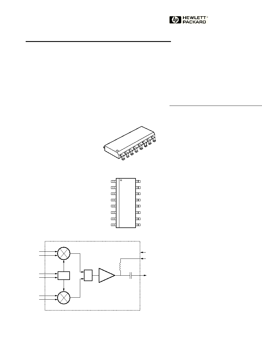
- Functional Block Diagram
- Plastic SO-16 Package
- Pin Configuration
- Description
- HPMX-2003 Absolute Maximum Ratings, TA = 25∞C
- HPMX-2003 Guaranteed Electrical Specifications, TA = 25∞C, ZO = 50 W
- HPMX-2003 Summary Characterization Information, TA = 25∞C, ZO = 50 W
- HPMX-2003 Pin Description
- HPMX-2003 Typical Data Measurement
- HPMX-2003 Typical Performance
- HPMX-2003 Single and Double Sideband Performance
- HPMX-2003 Typical Sideband Performance Data
- HPMX-2003 Using Offsets to Improve LO Leakage
- HPMX-2003 Modulation Spectrum Diagrams
- HPMX-2003 GSM
- HPMX-2003 Typical Performance Data
- HPMX-2003 NADC
- HPMX-2003 JDC
- HPMX-2003 Typical Performance Data
- HPMX-2003
- Package Dimensions SO-16 Package
- HPMX-2003 Test Board Layout
7-38
Silicon Bipolar RFIC
900 MHz Vector Modulator
Technical Data
HPMX-2003
Features
∑ 800≠1000 MHz Output
Frequency Range
∑ +6 dBm Peak P
out
∑ Unbalanced 50
Output
∑ Internal 90
∞
Phase Shifter
∑ 5 Volt, 36 mA Bias
∑ SO-16 Surface Mount Package
Applications
∑ Direct Modulator for 900
MHz Cellular Telephone
Handsets, Including GSM,
JDC, and NADC
∑ Direct Modulator for
900 MHz ISM Band Spread-
Spectrum Transmitters and
LANs
Functional Block Diagram
Pin Configuration
Plastic SO-16 Package
Description
Hewlett Packard's HPMX-2003 is a
Silicon RFIC direct conversion
vector modulator designed for use
at output frequencies between
800 MHz and 1 GHz. Housed in a
SO-16 surface mount plastic pack-
age, the IC contains two matched
Gilbert cell mixers, an RC phase
shifter, a summer, and an output
amplifier complete with 50
impedance match and DC block.
This device is suitable for use in
direct and offset-loop modulated
portable and mobile telephone
handsets for cellular systems such
as GSM, North American Digital
Cellular and Japan Digital Cellu-
lar. It can also be used in digital
transmitters operating in the
900 MHz ISM (Industrial-Scien-
tific-Medical) band, including use
in Local Area Networks (LANs).
The HPMX-2003 is fabricated with
Hewlett-Packard's 25 GHz
ISOSAT-II process, which
combines stepper lithography,
ion-implantation, self-alignment
techniques, and gold metallization
to produce RFICs with superior
performance, uniformity and
reliability.
Iref
Q MIXER
V
CCL
RFout
I MIXER
Imod
LO +
Qmod
Qref
LO ≠
SUMMER
V
CC
50
Z
O
unbalanced
OUTPUT
AMPLIFIER
0
∞
90
∞
PHASE
SHIFTER
∑
16 VCCL
15 RFout
14 GROUND
13 GROUND
12 Iref
11 Imod
10 GROUND
9 DO NOT CONNECT
VCC 1
VCC 2
GROUND 3
GROUND 4
Qmod 6
LOin 7
LOgnd 8
Qref 5
5965-9103E

7-39
HPMX-2003 Guaranteed Electrical Specifications,
T
A
= 25
∞
C, Z
O
= 50
V
CC
= 5 V, LO= -12 dBm at 900 MHz (Unbalanced Input), V
Iref
= V
Qref
= 2.5 V (Unless Otherwise Noted).
Symbol
Parameters and Test Conditions
Units
Min.
Typ.
Max.
I
d
Device Current
mA
36
44
P
out
Output Power
V
Imod
= V
Qmod
= 3.75 V
dBm
+4.0
+6
LO
leak
P
out
- LO at Output
V
Imod
= V
Qmod
= 2.5 V
dBc
+30
+37
mod
Average
%
4
7
Modulation
Error
Thermal Resistance
[2]
:
jc
=125
∞
C/W
Notes:
1. Operation of this device above any one
of these parameters may cause
permanent damage.
2. T
C
= 25
∞
C (T
C
is defined to be the
temperature at the end of pin 3 where it
contacts the circuit board).
3. Derate at 8 mW/
∞
C for T
C
> 88
∞
C.
4. Do not exceed V
CC
by more than 0.8 V.
HPMX-2003 Absolute Maximum Ratings,
T
A
= 25
∞
C
Absolute
Symbol
Parameter
Units
Maximum
[1]
P
diss
Power Dissipation
[2,3]
mW
500
LO
in
LO Input Power
dBm
15
V
CC
Supply Voltage
V
10
V
Imod
,
Swing of V
Imod
about V
Iref
[4]
V
p-p
5
[4]
V
Qmod
or V
Qmod
about V
Qref
V
Iref
, V
Qref
Reference Input Levels
[4]
V
5
[4]
T
STG
Storage Temperature
∞
C
-65 to +150
T
j
Junction Temperature
∞
C
150
HPMX-2003 Summary Characterization Information,
T
A
= 25
∞
C, Z
O
= 50
V
CC
= 5 V, LO = -12 dBm at 900 MHz (Unbalanced Input), V
Iref
= V
Qref
= 2.5 V (Unless Otherwise Noted).
Symbol
Parameters and Test Conditions
Units
Typ.
R
in
Input Resistance (I
mod
to I
ref
or Q
mod
to Q
ref
)
10 k
R
in-gnd
Input Resistance to Ground (Any I, Q Pin to Ground)
10 k
VSWR
LO
LO VSWR (50
)
GSM: 890-915 MHz Bandwidth
1.5:1
NADC: 824-850 MHz Bandwidth
1.5:1
JDC: 940-960 MHz Bandwidth
1.5:1
VSWR
O
Output VSWR (50
) (Tuned by
GSM: 890-915 MHz Bandwidth
1.2:1
Placement of V
ccL
Capacitor ≠
NADC: 824-850 MHz Bandwidth
1.1:1
See Figures 22, 32, and 42)
JDC: 940-960 MHz Bandwidth
1.2:1
Output Noise Floor
V
Imod
= V
Qmod
= 3.75 V
dBm/Hz
-134
IM
3
DSB Third Order Intermodulation Products
dBc
+34
A
i
RMS Amplitude Error
dB
0.3
P
i
RMS Phase Error
degrees
2
(V
Imod
- 2.5)
2
+ (V
Qmod
- 2.5)
2
= 1.25 V
7-40
lar performance. The recom-
mended level of unbalanced I and
Q signals is 2.5 V
p-p
with an aver-
age level of 2.5 V above ground.
The reference pins should be DC
biased to this average data signal
level (V
CC
/2 or 2.5 V typ.). For
single ended drive, pins 5 and 12
can be tied together. For balanced
operation, 2.5 V
p-p
signals may be
applied across the I
mod
/I
ref
and the
Q
mod
/Q
ref
pairs. The average level
of all four signals should be about
2.5 V above ground. The imped-
ance between any I or Q
and
ground is typically 10 K
and the
impedance between I
mod
and I
ref
or
Q
mod
and Q
ref
is typically 10 K
.
The input bandwidth typically
exceeds 40 MHz. It is possible to
reduce LO leakage through the IC
by applying slight DC imbalances
between I
mod
and I
ref
and/or Q
mod
and Q
ref
(see section entitled
"HPMX-2003 Using Offsets to Im-
prove Lo Leakage"). All perfor-
mance data shown on this data
sheet was taken with unbalanced
I/Q inputs.
LO Input (pins 7 and 8)
The LO input of the HPMX-2003 is
balanced and matched to 50 For
drive from an unbalanced LO, pin
7 should be AC coupled to the LO
Figure 1. HPMX-2003 Connections Showing Unbalanced LO
and I, Q Inputs.
Figure 2. HPMX-2003 Connections Showing Balanced LO
and I, Q Inputs.
HPMX-2003 Pin
Description
V
CC
(pins 1,2)
These two pins provide DC power
to the mixers in the RFIC, and are
connected together internal to the
package. They should be con-
nected to a 5 V supply, with appro-
priate AC bypassing (1000 pF typ.)
used near the pins, as shown in
figures 1 and 2. The voltage on
these pins should always be
kept at least 0.8 V more posi-
tive than the DC level on any
of pins 5, 6, 11, or 12. Failure to
do so may result in the modulator
drawing sufficient current
through the data or reference
inputs to damage the IC.
Ground (pins 3, 4, 10, 13 & 14)
These pins should connect with
minimal inductance to a solid
ground plane (usually the back-
side of the PC board). Recom-
mended assembly employs
multiple plated through via holes
where these leads contact the PC
board.
I
ref
(pin 12) and Q
ref
(pin 5),
I (pin 11) and Q (pin 6) Inputs
The I and Q inputs are designed
for unbalanced operation but can
be driven differentially with simi-
using a 50
transmission line and
a blocking capacitor (1000 pF
typ.), and pin 8 should be AC
grounded (1000 pF capacitor
typ.), as shown in figure 1. For
drive from a balanced LO source,
50
transmission lines and block-
ing capacitors (1000 pF typ.) are
used on both pins 7 and 8, as
shown in figure 2. The internal
phase shifter allows operation
from 800 - 1000 MHz. The recom-
mended LO input level is -12 dBm.
All performance data shown on
this data sheet was taken with un-
balanced LO operation.
RF Output (pin15)
The RF output of the HPMX-2003
is configured for unbalanced
operation. The output is internally
DC blocked and matched to 50
,
so a simple 50
microstrip line is
all that is required to connect the
modulator to other circuits.
V
CCL
(pin 16)
Pin 16 is the V
CC
input for the out-
put stage of the IC. It is not inter-
nally connected to the other V
CC
pins. The external connection al-
lows the addition of a small induc-
tor (0 - 6 nH) to tune the output
for minimum VSWR, depending
upon the operating frequency.
DO NOT CONNECT
LO
in
1000 pF
1000 pF
+5 V
RFout
1000 pF
Qref
Qmod
Iref
Imod
OPTIONAL INDUCTOR
1000 pF
1
2
6
5
8
16
12
11
3
4
7
9
10
13
14
15
DO NOT CONNECT
LO
in+
1000 pF
1000 pF
+5 V
RFout
Qmod
Imod
LO
in≠
1000 pF
Qref
I ref
OPTIONAL INDUCTOR
1000 pF
1
2
6
5
8
16
12
11
3
4
7
9
10
13
14
15
7-41
HPMX-2003 Typical Data
Measurement
Direct measurement of the ampli-
tude and phase error at the output
is an accurate way to evaluate
modulator performance. By mea-
suring the error directly, all the
harmonics, LO leakage, etc. that
show up in the output signal are
accounted for. Figure 3, below,
shows the test setup that was used
to create the amplitude and phase
error plots (figures 12 and 13).
Amplitude and phase error are
measured by using the four chan-
nel power supply to simulate I and
Q input signals. Real 2.5 V
p-p
I and
Q signals would swing 1.25 volts
above and below an average 2.5 V
level, therefore, a "high" level in-
put is simulated by applying
3.75 V, and a "low" level by apply-
ing 1.25 V to the I and/or Q inputs.
bling phase readings on the net-
work analyzer.
The same test setup shown below
is used to measure input and out-
put VSWR, reverse isolation, and
power vs. frequency. V
Imod
and
V
Qmod
are set to 3.75 V and the
appropriate frequency ranges are
swept. S
11
provides input VSWR
data, S
22
provides output VSWR
data. S
21
provides power output
(add source power to S
21
derived
gain).
LO leakage data shown in figures
18, and 19 is generated by setting
V
Imod
= V
Qmod
= V
Iref
= V
Qref
= 2.5 V
then performing an S
21
sweep.
Since phase is not important for
these measurements, a scalar net-
work analyzer or a signal genera-
tor and spectrum analyzer could
be used.
Amplitude and phase are
measured by setting the network
analyzer for an S
21
measurement
at frequency of choice. Set the
port 1 stimulus level to the LO
level you intend to use in your cir-
cuit (-12 dBm for the data sheet).
A 6-10 dB attenuator can be
placed in the line to port 2 to pre-
vent network analyzer overload,
depending upon the network ana-
lyzer you are using.
By adjusting the V
Imod
and V
Qmod
settings you can step around the
I, Q vector circle, reading mag-
nitude and phase at each point.
The relative values of phase and
amplitude at the various points
will indicate the accuracy of the
modulator. Note: you must use
very low ripple power supplies
for the reference, V
Imod
, and V
Qmod
supplies. Ripple or noise of only a
few millivolts will appear as wob-
Figure 3. Test Setup for Measuring Amplitude and Phase Error, Input and Output
VSWR, Power Output and LO Leakage of the Modulator.
HP-6626A
SYSTEM DC POWER SUPPLY
(FOUR OUTPUTS)
5 V
VQmod
VImod
2.5 V
HP-8753C VECTOR NETWORK ANALYZER
PORT 1
PORT 2
LO
Q
R
VCC
5 V
OUT
R
C
C
C
H
VER 1
I
HPMX-2003/5
C
7-42
HPMX-2003 Typical Performance
Figure 9. HPMX-2003 LO Input VSWR
vs. Frequency and Temperature,
V
CC
= 5 V.
Figure 10. HPMX-2003 Output VSWR
vs. Frequency and Temperature.
Figure 11. HPMX-2003 Output VSWR
vs. V
CC
at 900 MHz, T
A
= 25
∞
C.
Figure 4. HPMX-2003 Device Current
vs. Temperature, V
CC
= 5 V.
Figure 5. HPMX-2003 Device Current
vs. V
CC
, T
A
= 25
∞
C.
Figure 6. HPMX-2003 Power Output
vs. Temperature at 900 MHz,
LO = -12 dBm, V
Imod
= V
Qmod
= 3.75 V,
V
Iref
= V
Qref
= 2.5 V, V
CC
= 5 V.
Figure 7. HPMX-2003 Power Output
vs. V
CC
and I, Q Level at 900 MHz,
LO = -12 dBm, V
Imod
= V
Qmod
, T
A
= 25
∞
C.
Figure 8. HPMX-2003 Power Output
vs. LO Level at 900 MHz, V
CC
= 5 V,
V
Imod
= V
Qmod
= 3.75 V , T
A
= 25
∞
C.
5
33
-55
TEMPERATURE (
∞
C)
30
36
-35
-15
39
45
42
DEVICE CURRENT (mA)
25
45
65
85
5
30
4
V
CC
(VOLTS)
25
35
4.5
40
50
45
DEVICE CURRENT (mA)
5.5
6
5
2
-55
TEMPERATURE (
∞
C)
0
4
-35
-15
6
10
8
OUTPUT POWER (dBm)
25
45
65
85
5
-4
4
V
CC
(VOLTS)
-10
0
4.5
4
10
6
OUTPUT POWER (dBm)
5.5
6
-8
4.25 V
3.75 V
3.25 V
3.0 V
2.75 V
4.25
4.75
5.25
5.75
-6
-2
2
8
2
-25
LO INPUT POWER (dBm)
0
4
-20
6
10
8
OUTPUT POWER (dBm)
-15
-10
-5
0
2:1
750
FREQUENCY (MHz)
1:1
850
3:1
5:1
4:1
INPUT VSWR
950
1050
-55
∞
C
85
∞
C
2:1
750
FREQUENCY (MHz)
1:1
850
3:1
5:1
4:1
OUTPUT VSWR
950
1050
-55
∞
C
85
∞
C
5
1.2:1
4
V
CC
(VOLTS)
1:1
1.4:1
4.5
1.6:1
2:1
1.8:1
OUTPUT VSWR
5.5
6