 | –≠–ª–µ–∫—Ç—Ä–æ–Ω–Ω—ã–π –∫–æ–º–ø–æ–Ω–µ–Ω—Ç: HPMX-2006 | –°–∫–∞—á–∞—Ç—å:  PDF PDF  ZIP ZIP |
Document Outline
- List of Figures
- 1. Mixer Device Current vs. Device Voltage over Temperature
- 2. Mixer Device Current vs. Device Voltage over Temperature
- 3. Amp. Output at P in = 9.5 dBm and at 1 dB Compression and Small Signal Gain vs. Temperature
- 4. Mixer Output at V if = 30 mV pp
- 5. Mixer Output at V if = 30 mV pp
- 6. Mixer Output at V if = 30 mV pp
- 7. Mixer Output Spectrum for 1 GHz Bandwidth, Centered at 1900 MHz.
- 8. Impedance of Mixer IF Port.
- 9. Impedance of Mixer LO Port.
- 10. Impedance of Mixer RF Port
- 11. Test Board Configuration.
- 12. Schematic Diagram of Typical IC Use.
- 13. Mixer Only Use (AC
- 14. 900 MHz Use. Refer to Table 2 for Component Values
- 15. LO Connections for Single-ended Operation
- 16. LO Connections for Balanced Operation
- 17. IF Connections for AC Coupled Single-ended Use.
- 18. IF Connections for AC Coupled Balanced Use.
- 19. IF Connections for DC Coupled Use
- List of Tables
- 1. Typical Output Spurs for 0 Ö 6 GHz, Standard Test Conditions.
- 2. Values for Variable Components (see next page for details).
- 3. Amp Output Match Component Values
- 4. Vbase vs. Vcc . Vbase is the required bias at the IF ports
- Features
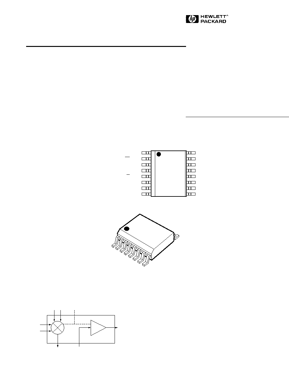
- Package Pin Configuration
- Applications
- Functional Block Diagram
- Package Pin Configuration
- Plastic SSOP-16
- Description
- HPMX-2006 Absolute Maximum Ratings [1]
- Standard Test Conditions
- HPMX-2006 Guaranteed Electrical Specifications
- HPMX-2006 Summary Characterization Information
- HPMX-2006 Pin Description Table
- HPMX-2006 Typical Performance
- HPMX-2006 Mixer Port Impedances
- HPMX-2006 Circuit Use
- Typical Scattering Parameters, Common Emitter, ZO = 50 W, VCC =3 V, IC = 23 mA
- HPMX-2006 Test Circuit
- HPMX-2006 Circuit Use
- Part Number Ordering Information
- Package Dimensions
7-66
0.8 ≠ 2.5 GHz
Upconverter/Amplifier
Technical Data
Features
∑ Wide Band Operation
RF Output: 800 -2500 MHz
IF Input: DC- 900 MHz
∑ 2.7- 5.5 V Operation
∑ Mixer + Amplifier: 38 mA
Mixer only: 15 mA
Standby Mode: <40
µ
A
∑ Differential LO and High
Impedance IF Inputs
∑ -8.5 dBm Mixer and
+4.5 dBm Amplifier Output
Power at 1900 MHz
∑ JEDEC Standard SSOP-16
Surface Mount Package
Applications
∑ Cordless Handsets and Base
Stations
∑ Wireless Data Terminals
∑ Cellular/ PCS Handsets and
Base Stations
HPMX-2006
Functional Block Diagram
LO
INPUT
IF INPUT
RF OUTPUT
AMP INPUT
AMP
OUTPUT
HPMX-2006
ENABLE
Package Pin Configuration
Plastic SSOP-16
Description
The HPMX-2006 upconverter/
amplifier IC is designed to meet
the needs of cellular and PCS
telephone and wireless LAN
applications.
The IC consists of a Gilbert Cell
mixer optimized for upconversion
followed by a post-amplifier. The
mixer and amplifier are indepen-
dent allowing the insertion of a
sideband filter between the two.
The mixer is double balanced.
Both LO and IF inputs may be run
either single-endedly, or in
differential mode to reduce LO
leakage. LO inputs are matched
near 50
; high impedance IF
inputs allow the mixer to be used
as a BPSK modulator. An inte-
grated transformer on the mixer
RF port creates a single-ended,
matched to 50
output at
1900 MHz, and also reduces
common mode noise.
HPMX
2006
YYWW
LO in 1
LO in 2
Ref 3
IF in 4
IF in 5
Amp Ve1 6
Amp RF in 7
enable 8
16 Mixer Vc
15 Gnd
14 Amp Vc
13 Amp RF Out
12 Amp Ve2
11 Amp 1 Ve2
10 Gnd 1
9 Mixer RF Out
HPMX
2006
YYWW
5966-0455E

7-67
The amplifier features a single-
ended 50
match on the input
port. The open collector output is
easily matched with a simple
2 element network, providing
flexible use and good power
added efficiency. The amplifier
can be disabled to allow use of the
mixer alone, reducing the current
draw to around 15 mA. The entire
IC can be put into a standby mode
reducing current consumption to
under 40
µ
A from a 3V source.
The SSOP-16 package insures that
the IC occupies a minimal amount
of printed circuit board space.
The HPMX-2006 is manufactured
using Hewlett-Packard's 30 GHz
ISOSAT-II process which com-
bines stepper lithography, self
alignment, ion implantation
techniques and gold metalization
to produce state-of-the-art RFICs.
HPMX-2006 Absolute Maximum Ratings
[1]
Mixer
Amplifier
Symbol
Parameter
Units
Min.
Max.
Min.
Max.
V
CC
Supply Voltage
V
-0.2
8
-0.2
8
P
diss
Power Dissipation
[2,3]
mW
174
274
Single-Ended Input Mixer LO Voltage
V
V
C
+ 0.2
Single-Ended Input Mixer IF Voltage
V
V
C
+ 0.2
Amplifier Input RF Power
dBm
+5
T
j
Junction Temperature
∞
C
-40
+150
-40
+150
T
STG
Storage Temperature
∞
C
-40
+150
-40
+150
Notes:
1. Operation of this device in excess of any of these parameters may cause
permanent damage.
2. T
CASE
= 25
∞
C
3. Derate at 7 mW/
∞
C for T
CASE
>82
∞
C.
Recommended operating range of V
cc
= 2.7 to 5.5 V, T
a
= -40 to + 85
∞
C
Thermal Resistance
[2]
:
jc
= 150
∞
C/W
HPMX-2006 Guaranteed Electrical Specifications
Standard test conditions apply unless otherwise noted.
Symbol
Parameters and Test Conditions
Units
Min.
Typ.
Max.
I
C
mix
Sleep Mode Current, Mixer
µ
A
20
I
C
amp
Sleep Mode Current, Amplifier
µ
A
20
I
C
mix
Mixer Transmit Current
mA
15
18
I
C
amp
Amplifier Transmit Current
mA
23
28
P
out
SSB Output Power, Mixer Only
dBm
-11
-9
P
out
Output Power, Amplifier Only (-9.5 dBm in)
dBm
+2.5
+3.8
Standard Test Conditions
Unless otherwise stated, all test data was taken on packaged parts under the following conditions:
V
cc
= +3.0 VDC, Z
out
= 50
, ambient temperature T
a
= 25
∞
C
LO input: 1750 MHz, -3 dBm, single-ended
IF input: 150 MHz, 300 mV
p-p
, single-ended, terminated in a 50
pull-up resistor (R1R2 in Figure 11)
Z
out mixer
= Z
in amp
= 50
, Z
out amp
per Figure 11 ( (L=2.8 nH, C=2.2 pF)
See Figure 11 for test set-up schematic diagram.
7-68
HPMX-2006 Summary Characterization Information
Standard test conditions apply unless otherwise noted. Table 2 applies for 900 and 2500 MHz.
IF remains 150 MHz for all frequencies.
Performance vs. Frequency
900 MHz
1900 MHz
2500 MHz
Units
Mixer RF Output Power, V
if
= 300 mV
pp
-8
-9
-12.5
dBm
Mixer RF Output Power, V
if
= 30 mV
pp
-28
-28
-32
dBm
Mixer RF Output Power at 1 dB Gain Compression
-7
-8.5
-12
dBm
Mixer Output Third Order Intercept Point
+3
+2
-4
dBm
Mixer LO Suppression
25
21
18.5
dBc
Mixer Phase Noise (4 MHz offset)
-143
-144
-146
dBm/Hz
Amplifier RF Output Power at P
in
= -9.5 dBm
+9
+3.8
-2
dBm
Amplifier RF Output Power at 1 dB Gain Compression
+9
+4.5
+2.5
dBm
Amplifier Output Third Order Intercept Point
+19
+14
+12
dBm
Small Signal Amplifier Gain
21
14.5
9.5
dB
Amplifier Noise Figure
8.5
9
9.5
dB
Amplifier Input Return Loss
10.5
9.5
10.5
dB
Amplifier Output Return Loss
9.5
6.5
12
dB
Isolation, Mixer Output to Amplifier Input
32
30
30
dB
HPMX-2006 Pin Description Table
No. Mnemonic
Description
Typical Signal
Notes
1
LO
differential mi
xer LO
-3 dBm from single-ended,
LO identical to LObar.
2
LObar
input
50
source
DC present (needs Cbl).
3
Ref
internal voltage reference
Supplies base bias for
AC-coupled IF.
4
IF
differential mixer IF
-6 dBm from single-ended,
IF identical to IFbar.
5
IFbar
input
50 W source
Must bias per Table 3.
6
AmpVe1
ground
0 V or unconnected
Disconnect for mixer only
7
AmpRFin
amplifier input
-9.5 dBm from 50
source
DC present (needs Cbl)
8
Enable
chip (amp and mixer)
<0.4V disables
enable input
>2.5V enables IC
9
MxRFout
mixer RF output
-9.0 dBm into 50
load
At DC ground
10
gnd1
ground
0 V
11
Amp1Ve2
ground
0 V or unconnected
Disconnect for mixer only
12
AmpVe2
ground
0 V or unconnected
Disconnect for mixer only
13
AmpRFout amplifier output
+3 dBm into 50
load
DC present (needs Cbl).
RF match required.
14
AmpVc
amplifier Vcc input
3 V, 23 mA
15
gnd
ground
0 V
16
MxVc
mixer Vcc input
3 V, 15 mA
7-69
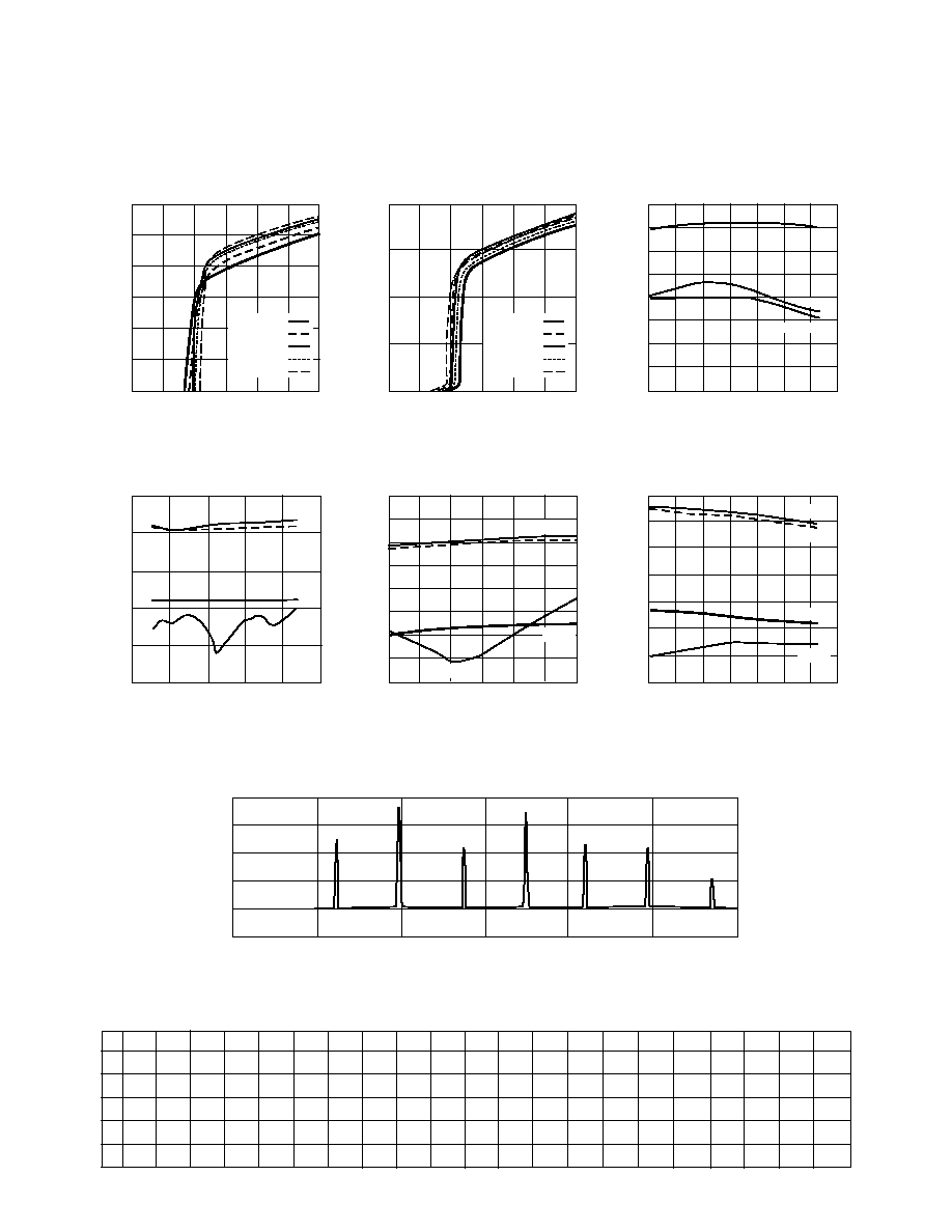
HPMX-2006 Typical Performance
Standard test conditions apply unless otherwise noted.
0
2
3
1
4
5
6
VOLTAGE (V)
Figure 1. Mixer Device Current vs.
Device Voltage over Temperature.
0
10
5
20
15
25
30
CURRENT (mA)
-40
0
20
40
-20
60
80
100
TEMPERATURE (
∞
C)
Figure 3. Amp. Output at P
in
= 9.5 dBm
and at 1 dB Compression and Small
Signal Gain vs. Temperature.
0
1
2
3
8
4
0
16
8
POWER
(dBm)
GAIN
(dB)
5
6
7
-35
-30
-20
-25
-10
-15
-40
20
40
60
-20
0
80
100
TEMPERATURE (
∞
C)
Figure 6. Mixer Output at V
if
= 30 mV
pp
and 300 mV
pp
, at P
1dB
, and LO
Suppression at V
if
= 300 mV
pp
vs.
Temperature.
-40
-5
POWER (dBm)
Figure 4. Mixer Output at V
if
= 30 mV
pp
and 300 mV
pp
, at P
1dB
, and LO
Suppression at V
if
= 300 mV
pp
vs. IF
Frequency.
Figure 2. Mixer Device Current vs.
Device Voltage over Temperature.
-10
-8
-2
0
2
-6
-4
LO POWER (dBm)
Figure 5. Mixer Output at V
if
= 30 mV
pp
and 300 mV
pp
, at P
1dB
, and LO
Suppression at V
if
= 300 mV
pp
vs. LO
Power.
-40
-30
-35
-20
-25
-10
-15
0
5
POWER (dBm)
Gss
T
A
= +85
∞
C
T
A
= +50
∞
C
T
A
= +25
∞
C
T
A
= +0
∞
C
T
A
= ≠ 40
∞
C
T
A
= +85
∞
C
T
A
= +50
∞
C
T
A
= +25
∞
C
T
A
= +0
∞
C
T
A
= ≠ 40
∞
C
0
2
3
1
4
5
6
VOLTAGE (V)
CURRENT (mA)
0
5
10
15
20
P 1dB
Pin = -9.5 dBm
-40
-30
-20
-10
0
600
800
200
400
1000
FREQUENCY (MHz)
-50
0
POWER (dBm)
P 1dB
300 mV
30 mV
LO lkg
300 mV
P 1dB
30 mV
LO lkg
300 mV
P 1dB
30 mV
LO lkg
1200
-100
-80
-60
-40
-20
0
1600
1800
2000
2200
2400
1400
FREQUENCY (MHz)
POWER (dBm)
Figure 7. Mixer Output Spectrum for 1 GHz Bandwidth, Centered at 1900 MHz.
Table 1. Typical Output Spurs for 0 ≠ 6 GHz, Standard Test Conditions.
-10
-9
-8
-7
-6
-5
-4
-3
-2
-1
0
1
2
3
4
5
6
7
8
9
10
0
-
-38.9 -32.2 -44.1 -49.3 -67.2 -64.4 <-80 -73.6 <-80 <-80
1 <-80 <-80 <-80
-70
-78.5 -52.1 -58.8 -33.2 -38.9 -10.1 -31.7 -8.7 -38.3 -38.3 -59.0 -50.1 -39.2 -50.1 -50.2 <-60 <-60
2 <-80 <-60 <-60 <-60 <-60 <-60 -49.5 -50.0 -33.2 -39.1 -42.1 -50.4 -36.1 -48.8 -58.8 <-60
<-60 <-60 <-60 <-60 <-60
3 <-60 <-60 -38.4 -58.6 <-60 <-60 <-60 -52.7 <-60 <-60 -45.6 -37.1
-52
<-60 <-60
4 <-60 -45.5 -52.0 <-60
7-70
HPMX-2006 Mixer Port Impedances
GHz
Mag.
Deg.
0.05
0.86
-4
0.10
0.81
-3
0.15
0.84
-1
0.20
0.88
-3
0.25
0.93
-9
0.30
0.91
-15
0.40
0.80
-19
0.50
0.81
-23
0.60
0.80
-28
0.70
0.80
-30
0.80
0.85
-34
0.90
0.84
-39
GHz
Mag.
Deg.
0.50
[1]
0.49
-49
0.75
0.48
-63
1.00
0.46
-73
1.25
0.42
-82
1.50
0.40
-102
1.75
0.31
-114
1.75
[2]
0.24
-131
2.00
0.20
147
2.25
0.20
87
2.50
0.16
15
2.75
0.37
-131
3.00
0.53
168
GHz
Mag.
Deg.
0.50
0.60
82
0.75
0.55
38
1.00
0.52
-5
1.25
0.36
-35
1.50
0.18
-44
1.75
0.17
-17
2.00
0.20
5
2.25
0.24
13
2.50
0.28
17
2.75
0.34
12
3.00
0.37
3
Figure 8. Impedance of Mixer IF Port.
Circuit of Figure 11 with 1 k Pull up
Resistors for the IFs and LO and RF Ports
Terminated in 50
.
Figure 9. Impedance of Mixer LO Port.
[1] Circuit of Figure 11 with IF and RF
Ports Terminated in 50
.
[2] As above but LO RC combination in
Figure 11 changed from 12
and
12 pF to 0
and 2.7 pF (recommended
use for >1.75 GHz).
Figure 10. Impedance of Mixer RF
Port.
Circuit of Figure 11 with IF and LO Ports
Terminated in 50
.
Typical Scattering Parameters,
Common Emitter, Z
O
= 50
, V
CC
= 3 V, I
C
= 23 mA
Freq.
S
11
S
21
S
12
S
22
GHz
Mag.
Ang.
dB
Mag.
Ang.
dB
Mag.
Ang.
Mag.
Ang.
0.1
0.51
149
19.72
9.68
-26
-37.08
0.014
-43
0.91
-3
0.5
0.37
144
17.42
7.43
-49
-39.17
0.011
11
0.78
-16
0.8
0.37
120
16.56
6.73
-76
-43.10
0.007
1
0.80
-22
0.9
0.37
113
16.24
6.49
-85
-36.48
0.015
25
0.83
-23
1.0
0.39
104
15.99
6.30
-94
-40.00
0.010
22
0.84
-26
1.1
0.39
96
15.55
5.99
-101
-41.94
0.008
28
0.84
-29
1.2
0.40
88
15.16
5.73
-112
-47.96
0.004
118
0.84
-32
1.3
0.41
81
15.07
5.67
-120
-38.42
0.012
68
0.85
-33
1.4
0.40
75
14.50
5.31
-125
-40.92
0.009
85
0.87
-36
1.5
0.40
67
13.37
4.66
-134
-46.02
0.005
147
0.84
-40
1.6
0.38
62
12.69
4.31
-145
-33.98
0.020
99
0.85
-40
1.7
0.37
61
12.46
4.20
-148
-33.15
0.022
102
0.84
-44
1.8
0.36
58
11.64
3.82
-153
-32.77
0.023
102
0.84
-49
1.9
0.33
62
11.17
3.62
-161
-34.42
0.019
88
0.79
-51
2.0
0.33
62
10.81
3.47
-168
-34.89
0.018
91
0.77
-54
2.1
0.31
64
9.99
3.16
-175
-29.37
0.034
96
0.75
-58
2.2
0.31
70
9.37
2.94
178
-30.75
0.029
102
0.72
-62
2.3
0.30
75
8.66
2.71
173
-30.75
0.029
89
0.69
-65
2.4
0.32
79
8.10
2.54
170
-33.15
0.022
90
0.67
-70
2.5
0.32
84
7.16
2.28
166
-32.77
0.023
89
0.65
-76
3.0
0.32
94
4.45
1.67
134
-28.40
0.038
99
0.49
-103