Document Outline
- List of Figures
- 1. I CC vs. Temperature.
- 2. Modulator + Mixer I CC vs. Temperature and Vcc
- 3. Modulator Only Mode I CC vs. Vcc. . .
- 4. Modulator + Mixer I CC vs. . .
- 5. Modulator Only SSB Performance vs. Vcc
- 6. Modulator Only SSB Performance vs. Temperature
- 7. Modulator Only DSB Output Power Level. . .
- 8. Modulator Only SSB Mode Performance. . .
- 9. Modulator Only SSB Output Power. . .
- 10. Modulator Only SSB Performance vs. LOmod Input Level
- 11. Modulator Only SSB Performance. . .
- 12. Modulator Only SSB Output Spectrum at 150 MHz
- 13. Modulator + Mixer SSB Output Levels vs. Vcc.
- 14. Modulator + Mixer SSB Output Levels vs. LOmix Power Input
- 15. Modulator + Mixer SSB Output Levels vs. Temperature and Vcc.
- 16. Modulator + Mixer SSB Output Levels vs. LOmod Power Input.
- 17. Modulator + Mixer SSB Performance. . .
- 18. Modulator + Mixer SSB Output Spectrum at 900 MHz
- 19. Modulator + Mixer DSB Performance. . .
- 20. Modulator Mixer SSB Performance. . .
- 21. Modulator + Mixer SSB Output Spectrum. . .
- 22. Modulator + Mixer SSB Output Spectrum
- 23. Modulator + Mixer SSB Output Spectrum. . .
- 24. Modulator + Mixer SSB Output Spectrum at 4000 MHz
- 25. Test Board Schematic Diagram. Connecting the Mixer Off Line to +3 V Turns Off the Mixer.
- 26. Equivalent Circuits for HPMX-2007 Inputs/Outputs.
- List of Tables
- 1. Typical Output Spurs.
- 2. Test Board Component Values that Change with Operating Frequency.
- Features
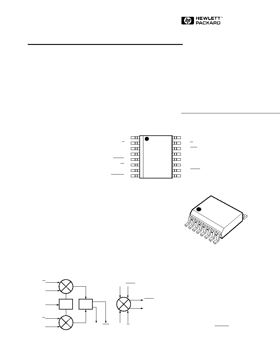
- Functional Block Diagram
- Package Pin Configuration
- Applications
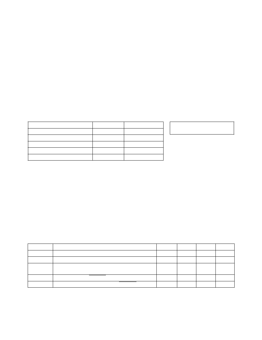
- Plastic SSOP-16
- General Description
- HPMX-2007 Absolute Maximum Ratings [1]
- Standard Test Conditions
- HPMX-2007 Key Guaranteed Electrical Specifications
- HPMX-2007 Summary Characterization Information
- HPMX-2007 Pin Description Table
- Package Dimensions
- Part Number Ordering Information
7-74
i
i
LOmod
q
q
MOD MOD
IF
IF
LOmix LOmix
RFOUT
RFOUT
Vector Modulator/Mixer
Technical Data
HPMX-2007
Package Pin Configuration
Features
� 5 MHz to 4 GHz Overall
Operating Frequency Range
� 40-400 MHz LOmod range
� 2.7 - 5.5 V Operation (3 V,
25 mA)
� Differential High Impedance
i, q Inputs
� On-Chip Linear RC Phase
Shifter
� -23 dBm Modulator S.E.
Output Power into 50
at
150 MHz
� -15 dBm Linear (-11 dBm
Saturated) Mixer Output
Power into 50
at 1900 MHz
� Mixer Can Be Used for
Up/Down Conversion or
Disabled (3 V, 10 mA)
� Standby Mode (<1
�
A)
� JEDEC Standard SSOP-16
Surface Mount Package
General Description
The HPMX-2007 vector
modulator/mixer IC is designed to
meet the needs of cellular and
PCS telephone applications.
The heart of the IC is a vector (or
quadrature) modulator followed
by a Gilbert cell mixer. The
modulator and mixer can be used
together, drawing only 25 mA
from a 3.0 volt supply. The mixer
can be disabled by connecting
either LOmix or LOmix to V
CC
,
Plastic SSOP-16
HPMX
2007
YYWW
i 1
i 2
LOmod 3
RF
OUT
4
RF
OUT
5
IF 6
IF 7
ENABLE 8
16 q
15 q
14 mod
13 mod
12 V
CC
11 V
EE
10 LOmix
9 LOmix/M IXOFF
HPMX
2007
YYWW
Functional Block Diagram
Applications
� NADC, PDC, GSM Handsets
and Base Stations
� PCS Handsets and Base
Stations
� DLMR Handsets
� CDPD Radios
� ISM Band Wireless Links
5965-7239E
7-75
allowing operation of the
modulator alone and reducing
current drain to only 10 mA.
The i and q signal inputs are
balanced to insure high common
mode noise rejection.
The output of the mixer is a
differential pair of open collectors.
One collector can be connected
to V
CC
and the other matched to
50
using a shunt L, series C
network. Alternatively, the output
can be matched to 50
through a
4:1 balun.
The SSOP-16 package insures that
the IC occupies a minimal amount
of printed circuit board space.
The HPMX-2007 is manufactured
using Hewlett-Packard's 30 GHz
ISOSAT-II process which
combines stepper lithography,
self alignment, ion implantation
techniques and gold metallization
to produce state-of-the-art RFICs.
Standard Test Conditions
Unless otherwise stated, all test data was taken on packaged parts under the following conditions:
V
CC
= +3.0 VDC, Z
out
= 50
, ambient temperature T
A
= 25
�
C
LOmod input: 149.67 MHz, 400 mV
p-p
, single ended
LOmix input: 1750.33 MHz, -10 dBm, single ended, 50
Single sideband tests:
i, q input: 10 kHz, 600 mV
p-p
differential with V
CC
/2 = 1.5 V offset.
See Figure 25 for test setup schematic diagram.
HPMX-2007 Key Guaranteed Electrical Specifications
Standard test conditions apply unless otherwise noted.
Symbol
Parameters and Test Conditions
Min.
Typ.
Max.
Units
P
out
SSB Output Power
-17.5
-15
dBm
Unwanted Sideband Output Level in SSB Mode
-40
-30
dBc
LOmix + LOmod Leakage Relative to SSB
-35
-27
dBc
Output Power
I
d
Device Current (ENABLE Open)
25
30
mA
Device Current, Disabled Mode (ENABLE = V
CC
)
5
25
�
A
HPMX-2007 Absolute Maximum Ratings
[1]
Recommended Operating Range of V
CC
= 2.7 to 5.5 V, T
A
= -
40 to +85
�
C.
Parameter
Min.
Max.
V
CC
Supply Voltage
8 V
Power Dissipation
[2,3]
400 mW
RF Input Power
+15 dBm
Junction Temperature
+150
�
C
Storage Temperature
-65
�
C
+150
�
C
Thermal Resistance:
[2]
jc
= 150
�
C/W
Notes:
1. Operation of this device in excess of
any of these parameters may cause
permanent damage.
2. T
case
= 25
�
C.
3. Derate at 7 mW/
�
C for T
case
> 90
�
C.
7-76
HPMX-2007 Pin Description Table
No.
Mnemonic
Description
Typical Signal
1
i
Balanced modulation input
600 mV pk-pk differential
2
i
3
LOmod
Modulator LO input
40-400 MHz, -10 dBm from
Z = 5 k
|| 0.5 pF
50
source
4
RF
Balanced mixer RF output open collectors
5-4000 MHz, 12 mA pk-pk differential,
5
RF
6
IF
Balanced mixer input
40-400 MHz, 350 mV pk-pk diff.
7
IF
8
ENABLE
Chip enable input
3 V CMOS logic compatible
9
LOmix/mixoff
10
LO1
11
V
EE
Chip substrate connection
0 V (DC and AC ground)
12
V
CC
Power supply connection
+2.7 - 5.5 V
13
MOD
Balanced modulator RF output
40-400 MHz, 2 mA pk-pk differential
14
MOD
15
q
Balanced modulation input
600 mV pk-pk differential
16
q
Z = 75 k
|| 0.5 pF
average value of V
CC
/2
Note: Impedances shown are AC equivalents at each pin, relative to ground. See Figure 26.
HPMX-2007 Summary Characterization Information
Standard test conditions apply unless otherwise noted.
Modulator-Only Mode
Typ
Units
DC Current Drain
10
mA
i, q Input 3 dB Bandwidth
>90
MHz
LOmod Input Frequency Range (for Sideband Suppression > 30 dBc)
40-400
MHz
SSB Output Current (Open Collectors). See Figure 26.
2
mA pk-pk diff.
SSB LOmod Suppression @ 150 MHz
-35
dBc
DSB 3rd Order IM Products @ 150 MHz
-45
dBc
Output Noise Floor
-160
dBm/Hz
Modulator + Mixer Performance (Output at 1900 MHz)
Typ
Units
Total DC Current Drain (Mixer Cannot Be Used Without Also
25
mA
Turning On the Modulator)
Mixer IF Input 3 dB Bandwidth
400
MHz
Differential Output Current (Open Collectors). See Figure 26.
12
mA pk-pk diff.
Linear Output Power. See Figure 25.
-15
dBm
IM
3
Output Power. See Figure 19.
-22
dBc
Output Noise Floor
-153
dBm/Hz
LOmix Leakage to RF Output
-22
dBc
with network shown in Figure 25
with network shown in Figure 25
-10 dBm from 50
source network
shown in Figure 25
average value of V
CC
/2
open collectors
Z = current src. || 35 k
|| 0.7 pF
Z = 75 k
|| 0.5 pF
Balanced mixer LO input and mixer
enable line
Z = 1 k
|| 0.6 pF
Z = 5 k
|| 0.5 pF
Z = current src. || 3 k
|| 0.7 pF
7-77
Table 1. Typical Output Spurs.
All values in dBc relative to output at 1900 MHz. f
LOmix
= 1750.33 MHz, f
LOmod
= 149.67 MHz, V
i
= V
q
= 1.65 V,
V
i
= V
q
= 1.35 V, f
spur
= m*f
LOmix
+n*f
LOmod
m
n
-6
-5
-4
-3
-2
-1
0
1
2
3
4
5
6
0
-38.8
-53.4
-47.7
-60.1
-46.7
-72.3
-
-72.2
-46.7
-60.1
-47.6
-53.3
-38.8
1
-51.9
-37.3
-37.7
-23.9
-23.6
0
-21.4
0
-22.1
-17.7
-41.7
-28.7
-35.1
2
-26.6
-32.8
-23.7
-36.3
-16.5
-34.5
-19.5
-21.3
-26.3
-36.8
-29.5
-48.8
-40.6
3
-37.8
-32.7
-57.4
-28.3
-25.9
-21.2
-27.5
-23.8
-38.7
-45.9
-54.3
-41.2
-48.8
4
-45.7
-47.1
-45.3
-47.0
-39.4
-51.1
-43.3
-40.4
-49.7
-54.7
-49.8
-57.8
-57.2
5
-65.0
-67.5
-56.1
-61.7
-57.6
-52.0
-43.5
-54.8
-61.6
-65.4
-59.9
-64.7
-63.7
6
-65.5
-82.2
-65.9
-60.7
-57.4
-62.7
-57.5
-66.2
-64.9
-77.1
-72.0
-83.1
-86.3
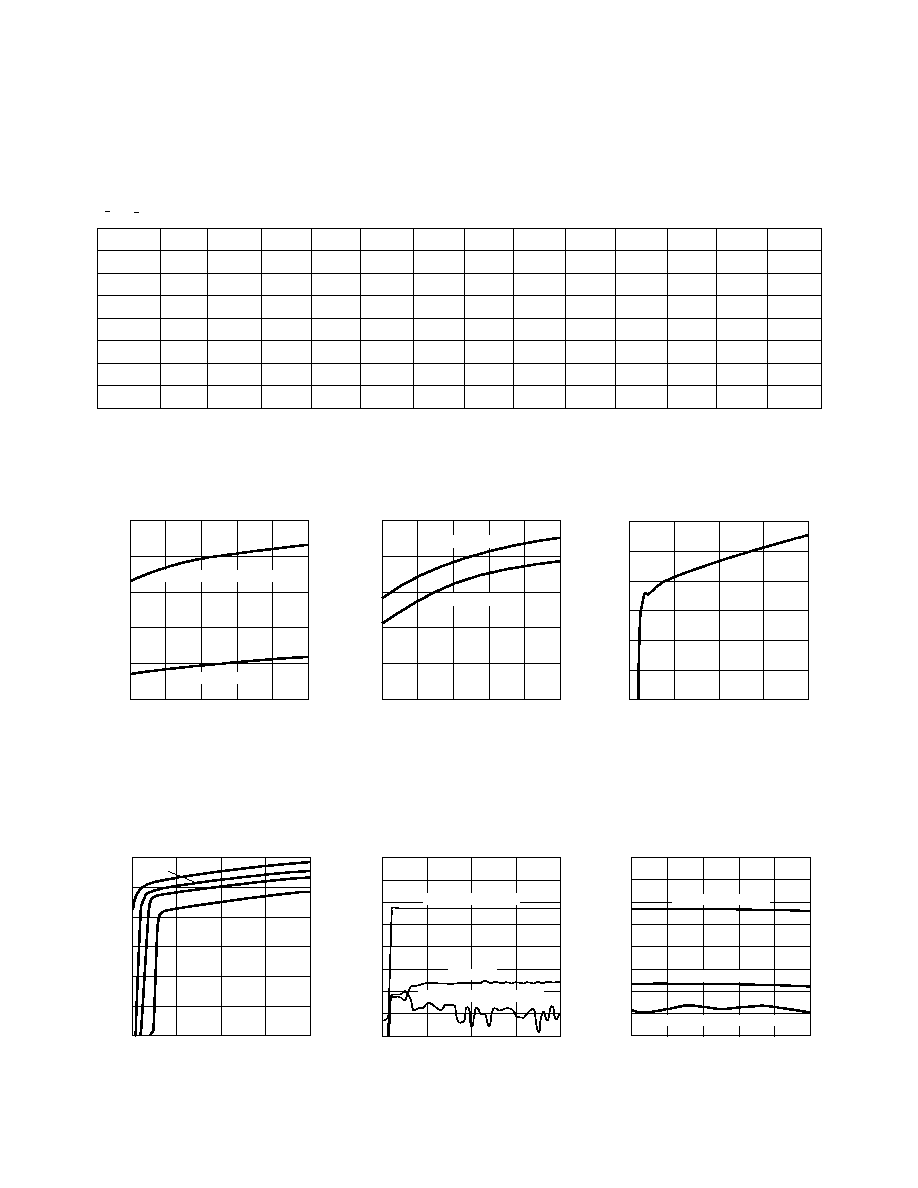
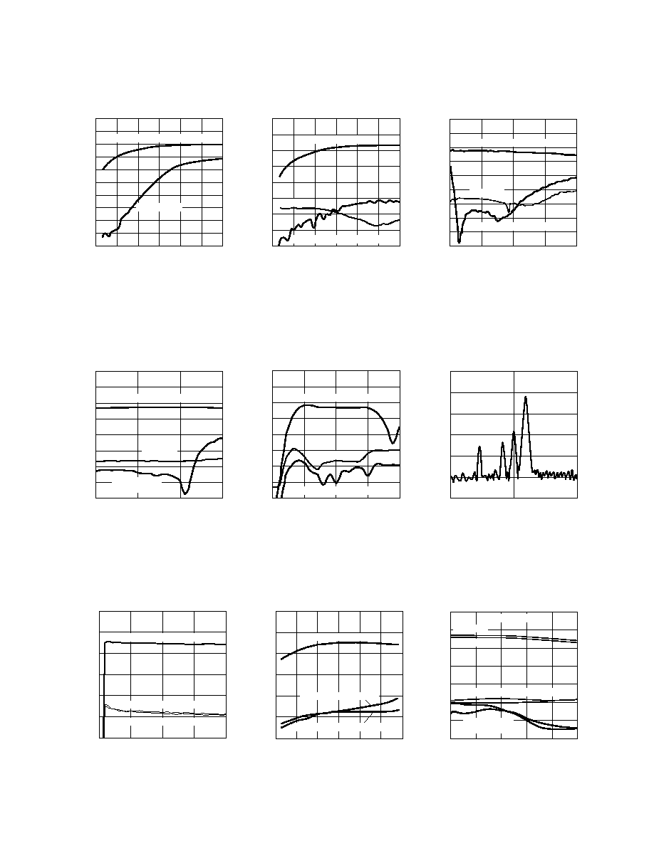
Figure 6. Modulator Only SSB
Performance vs. Temperature.
Figure 5. Modulator Only SSB
Performance vs. V
CC
.
Figure 4. Modulator + Mixer I
CC
vs.
V
CC
and Temperature.
OUTPUT LEVEL (dBm)
VCC (VOLTS)
3
0
4
6
-80
-30
2
-70
5
-50
-40
-10
-20
-60
SIDEBAND OUTPUT
CARRIER
SUPPRESSED SIDEBAND
TEMPERATURE (�C)
-15
10
60
85
-40
35
OUTPUT LEVEL (dBm)
0
-80
-30
-70
-50
-40
-10
-20
-60
SIDEBAND OUTPUT
CARRIER
SUPPRESSED SIDEBAND
Figure 2. Modulator + Mixer I
CC
vs.
Temperature and V
CC
.
Figure 1. I
CC
vs. Temperature.
Figure 3. Modulator Only Mode I
CC
vs. V
CC
at 25
�
C.
I CC
(mA)
TEMPERATURE (�C)
-15
30
10
60
85
5
25
-40
10
35
15
20
MODULATOR + MIXER
MODULATOR ONLY
I CC
(mA)
TEMPERATURE (�C)
-15
30
10
60
85
15
27
-40
18
35
21
24
VCC = 3 V
VCC = 5 V
I CC
(mA) MODULATOR ONLY @ 25 �C
VCC (VOLTS)
3
12
4
6
6
10
2
7
5
8
9
11
I CC
(mA)
VCC (VOLTS)
3
30
4
6
0
20
2
5
5
10
15
25
85 �C
-40 �C
0 �C
25 �C
7-78
OUTPUT LEVEL (dBm)
i,q AMPLITUDE (Vpk)
200
0
300
600
-100
-30
0
-70
500
-50
-40
-10
-20
-60
DSB OUTPUT (EACH SIDEBAND)
IM3 OUTPUT
100
400
-80
-90
OUTPUT LEVEL (dBm)
i,q AMPLITUDE (Vpk)
200
0
300
600
-80
-30
0
-70
500
-50
-40
-10
-20
-60
SIDEBAND OUTPUT
CARRIER
SUPPRESSED SIDEBAND
100
400
Figure 7. Modulator Only DSB Output
Power Level and IM3 Level vs. i,q
Input Amplitude (Each Pin, Relative
to Ground).
Figure 8. Modulator Only SSB Mode
Performance vs. i,q Input Amplitude
(Each Pin, Relative to Ground).
Figure 9. Modulator Only SSB Output
Power, Carrier and Sideband
Suppression vs. LOmod Frequency.
Figure 13. Modulator + Mixer SSB
Output Levels vs. V
CC
.
Figure 14. Modulator + Mixer SSB
Output Levels vs. LOmix Power Input.
Figure 15. Modulator + Mixer SSB
Output Levels vs. Temperature and V
CC
.
Figure 11. Modulator Only SSB
Performance vs. i,q Offset Level
(Each Pin, Relative to Ground).
Figure 10. Modulator Only SSB
Performance vs. LOmod Input Level.
1
1.5
2.5
0.5
2
0
-80
-30
-70
-50
-40
-10
-20
-60
OUTPUT LEVEL (dBm)
i,q OFFSET LEVEL (VOLTS)
SIDEBAND OUTPUT
CARRIER
SUPPRESSED SIDEBAND
OUTPUT LEVEL (dBm)
FREQUENCY (MHz)
0
149.67
149.725
-120
-40
149.615
-100
-80
-60
-20
TEMPERATURE (�C)
-15
10
60
85
-40
35
OUTPUT LEVEL (dBm)
0
-30
-70
-50
-40
-10
-20
-60
SIDEBAND OUTPUT
LOmix + LOmod LEAK
SUPPRESSED
SIDEBAND
VCC = 5 V
VCC = 3 V
OUTPUT LEVEL (dBm)
LOmix POWER INPUT (dBm)
-20
0
-10
5
-60
-20
-25
-50
0
-40
-30
-10
SIDEBAND OUTPUT
LOmix + LOmod LEAK
SUPPRESSED SIDEBAND
-15
-5
OUTPUT LEVEL (dBm)
VCC (VOLTS)
3
0
4
6
-60
-20
2
-50
5
-40
-30
-10
SIDEBAND OUTPUT
LOmix + LOmod LEAK
SUPPRESSED SIDEBAND
0
-80
-30
-70
-50
-40
-10
-20
-60
OUTPUT LEVEL (dBm)
LOmod INPUT POWER (dBm)
-15
-5
5
-25
SIDEBAND OUTPUT
CARRIER
SUPPRESSED
SIDEBAND
OUTPUT LEVEL (dBm)
LOmod FREQUENCY (MHz)
200
0
400
800
-90
-30
0
-80
600
-50
-40
-10
-20
-60
SIDEBAND OUTPUT
CARRIER
SUPPRESSED SIDEBAND
-70
Figure 12. Modulator Only SSB
Output Spectrum at 150 MHz.