Document Outline
- List of Figures
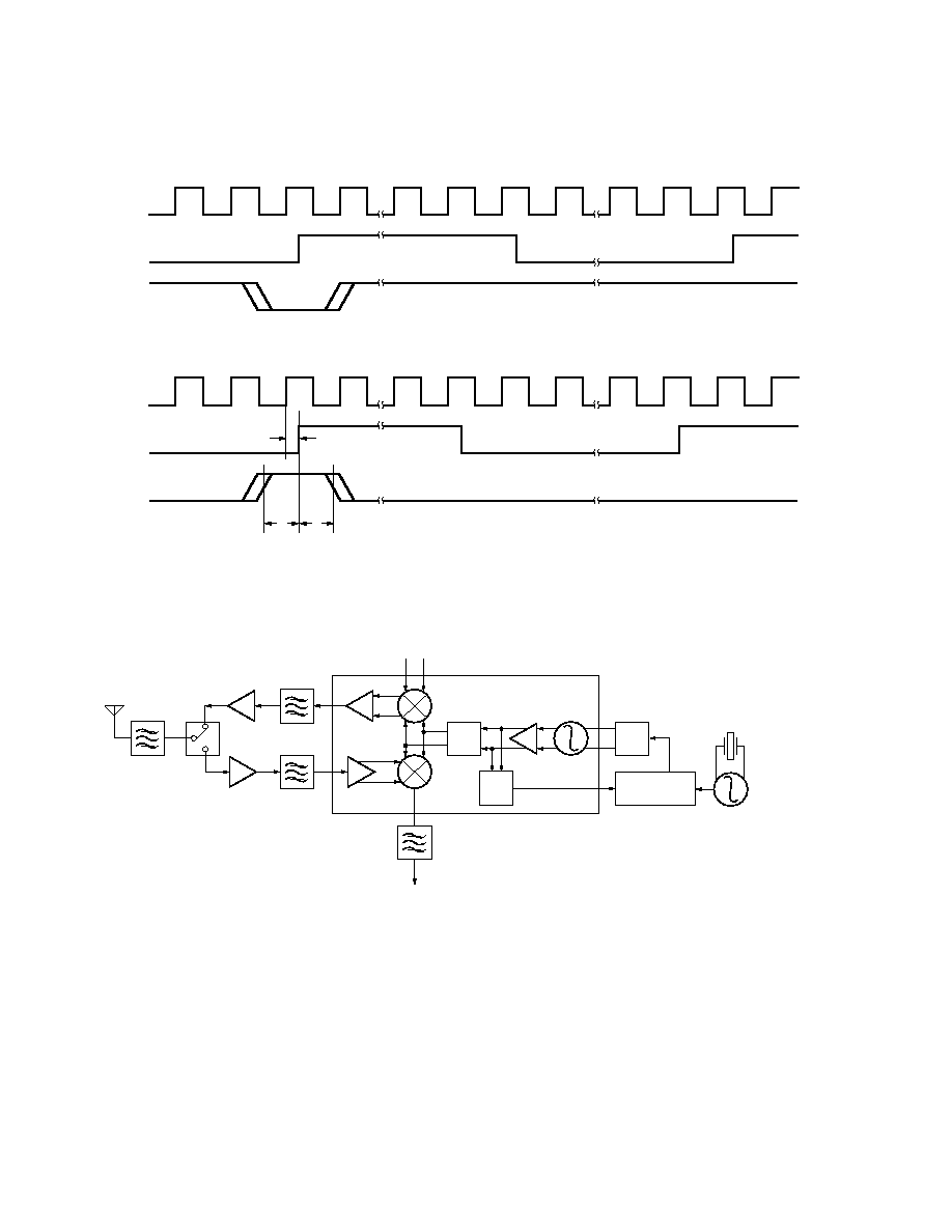
- 2. HPMX-5001 Prescaler Timing Diagram.
- 3. HPMX-5001 Block Diagram/Typical Application.
- 4. Typical HPMX-5001 Application with HPMX-5002 IF Chip. All Other Connections Go to Burst Mode Controller, Power Source, or...
- 5. I CC in Standby Mode vs. Temperature and V CC .
- 6. I CC in Receive Mode vs. Temperature and V CC .
- 7. I CC in Synthesizer Mode vs. Temperature and V CC .
- 8. I CC in Transmit Mode vs. Temperature and V CC .
- 9. Receive Downconverter Input VSWR vs. Temperature and V CC.
- 10. Receive Downconverter Output VSWR vs. Temperature and V CC .
- 11. Receive Downconverter SSB Noise Figure vs. Temperature and V CC.
- 12. Receive Downconverter Input Third Order Intercept Point and Output 1 dB Compression Point vs. Temperature and V CC .
- 13. Receive Downconverter Conversion Gain vs. Temperature and V CC.
- 14. 2 x f LO Leakage at Receive Downconverter Output vs. Temperature and V CC.
- 15. 2 x f LO Suppression at Transmit Upconverter Output vs. Temperature and V CC.
- 16. Transmit Upconverter Output VSWR vs. Temperature and V CC.
- 17. Carrier to Noise Ratio at Transmit Upconverter Output vs. Temperature and V CC .
- 18. Transmit Upconverter Power Output and Output 1 dB Compression Point vs. Temperature and V CC.
- 19. Prescaler Output Voltage vs. Temperature and V CC.
- 20. Equivalent Circuit and Recommended Output and Load Circuits for the HPMX-5001 Prescaler Output.
- 21. Equivalent Circuit for the Divider Modulus Control.
- 22. Equivalent Circuit for VCO Tank Connection and Recommended Tank Circuit.
- 23. Equivalent Circuit for Logic Control Pin 1, 31, and 32.
- 24. Equivalent Circuit for RXRF Input.
- 25. Equivalent Circuit for TXIF Input.
- 26. Equivalent Circuit for the RXIF Output and Recommended Matching Circuit for 110.592 MHz IF.
- 27. Equivalent Circuit for TXRF Output and Matching Network for DECT Phone Operation.
- 28. Test Board Schematic Diagram. All I/O Labels Correspond to Those on the Test board. See Table 3 for Component Values.
- List of Tables
- 1 - HPMX-5001 Pin Description
- 2 - HPMX-5001 Mode Control
- 3 - Test Board Components Shown in Figure 28.
- 4 - Component changes for dfferent IF frequencies.
- Features
- Applications
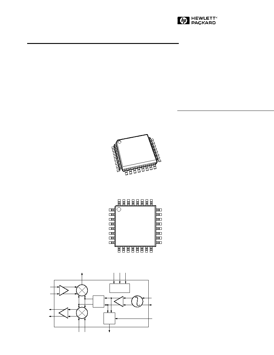
- Functional Block Diagram
- Plastic TQFP-32 Package
- Pin Configuration
- General Description
- HPMX-5001 Absolute Maximum Ratings [1]
- HPMX-5001 Guaranteed Electrical Specifications
- HPMX-5001 Summary Characterization Information
- Functional Description
- Part Number Ordering Information
- Package Dimensions 32 Pin Thin Quad Flat Package
- Tape Dimensions and Product Orientation for Outline TQFP-32
7-90
1.5 � 2.5 GHz Upconverter/
Downconverter
Technical Data
HPMX-5001
Features
� 2.7 V Single Supply Voltage
� Low Power Consumption
(60 mA in Transmit Mode,
39 mA in Receive Mode
Typical)
� 2 dBm Typical Transmit
Power at 1900 MHz
� Half-Frequency VCO with
Frequency Doubler
� 32/33 Dual-Modulus
Prescaler
� Flexible Chip Biasing,
Including Standby Mode
� TQFP-32 Surface Mount
Package
� Operation to 2.5 GHz
Applications
� DECT, UPCS and ISM Band
Handsets and Basestations
General Description
The HPMX-5001 Upconverter/
Downconverter provides RF
system designers with all of the
necessary features to perform an
RF-to-IF downconversion for a
receive path, as well as an IF-to-
RF upconversion for transmit
mode.
Designed to meet the unique
needs of portable applications,
the HPMX-5001 combines the
qualities of flexible chip biasing,
low power consumption, and true
2.7 V minimum supply voltage
operation to provide superior
performance and battery life. By
incorporating the active elements
of the VCO on-chip, as well as a
32/33 dual-modulus prescaler,
overall system component count
and costs are decreased. The
32-TQFP package insures that
this high level of integration
occupies a small amount of
printed circuit board space.
The HPMX-5001 can be used in
either dual-conversion systems
(with the HPMX-5002 IF
Demodulator/Modulator) or
single-conversion systems. The
HPMX-5001 is manufactured
using Hewlett-Packard's HP-25
Silicon Bipolar Process with
25 GHz f
T
and 30 GHz f
Max
.
Plastic TQFP-32 Package
Functional Block Diagram
X2
32/33
RX IF OUT
POWER DOWN
CONTROL
EXT.
VCO
TANK
RATIO
SELECT
TX IF IN
PRESCALER
OUT
RX RF IN
TX RF OUT
H
HPMX-5001
YYWW
XXXX ZZZ
Pin Configuration
H
HPMX-5001
YYWW
XXXX ZZZ
32
1
25
24
8
17
9
16
� Use with Companion
HPMX-5002 IF chip
5965-9105E
7-91
HPMX-5001 Absolute Maximum Ratings
[1]
Parameter
Min.
Max.
V
CC
Supply Voltage
-0.2 V
8 V
Voltage at Any Pin
[4]
-0.2 V
V
CC
+ 0.2 V
Power Dissipation
[2,3]
600 mW
RF Input Power
15 dBm
Junction Temperature
+150
�
C
Storage Temperature
-55
�
C
+125
�
C
HPMX-5001 Guaranteed Electrical Specifications
Unless otherwise noted, all parameters are guaranteed under the following conditions: V
CC
= 3.0 V. Test
results are based upon use of networks shown in test board schematic diagram (see Figure 28). Typical
values are for V
CC
= 3.0 V, T
A
= 25
�
C.
Symbol
Parameters and Test Conditions
Units
Min.
Typ.
Max.
G
C
Receive Conversion Gain
[1]
dB
12
14
P
out
Transmitter Power Output
Input
[2]
2:1 output VSWR
dBm
0
2
I
CC
Device Supply Current
Transmit Mode
mA
64
80
Receive Mode
mA
43
54
Synth Mode
mA
15
19
Standby Mode (with DIVMC Set High)
�
A
1
50
V
DIV
DIV Single-Ended Swing
[3]
V
PP
0.7
1
Notes:
1. 50
RF source, 100 MHz < I
F
< 300 MHz, 1.89 GHz RF. There is a 750
resistor on chip between RXIF and RXIFB (pins 3 and 4). A
matching network from 750
to 50
is used for this measurement. Insertion loss of the matching network is included in the net
conversion gain figure. See Figure 28.
2. Signal injected into P3 in Figure 28 is -12.5 dBm.
3. DIV output AC coupled into a 2 k
|| 10 pF load. See test board schematic diagram, Figure 28.
Thermal Resistance
[2]
:
jc
= 100
�
C/W
Notes:
1. Operation of this device in excess of
any of these parameters may cause
permanent damage.
2. T
CASE
= 25
�
C.
3. Derate at 10 mW/
�
C for T
CASE
> 90
�
C.
4. Except CMOS logic inputs � see
Summary Characterization Information
table.
7-92
HPMX-5001 Summary Characterization Information
Typical values measured on test board shown in Figure 28 at V
CC
= 3.0 V, T
A
= 25
�
C, RXIF = 110.592 MHz,
TXRF = 1.89 GHz, unless otherwise noted.
Symbol
Parameters and Test Conditions
Units
Typical
V
IH
CMOS Input High Voltage (Can Be Pulled
V
V
CC
- 0.8
up as High as V
CC
+ 7 V)
[1]
V
IL
CMOS Input Low Voltage
V
V
CC
- 1.9
I
IH
CMOS Input High Current
�
A
< 10
I
IL
CMOS Input Low Current
�
A
> -300
t
s
DIVMC Setup Time
[2,8]
ns
4
t
h
DIVMC Hold Time
[2,8]
ns
0
t
pd
DIV Propagation Delay
[2,8]
ns
< 7
Mode Switching Time
[3]
�
s
< 1
Receive Mode
1.89 GHz
2.45 GHz
Gc
Receive Conversion Gain
[9]
dB
14
13.5
NF
Noise Figure
[4]
dB
10
10
I
IP3
Input Third Order Intercept Point
dBm
-8
-9
I
P1dB
Input 1 dB Gain Compression Point
dBm
-18
-18
LO Leakage (2 x f
VCO
) at IF Port
dBm
-57
--
VSWR
in
Input VSWR
[5]
1.3:1
1.3:1
Transmit Mode
[6]
PIM
3
Power Output Level for >35 dB IM
3
Suppression
[10]
dBm
--
-5
O
P1dB
Output 1 dB Gain Compression Point
dBm
0
0
VSWR
out
Output VSWR
1.8:1
1.8:1
LO Suppression (2 x f
VCO
)
dBc
25
30
F
3dB
IF
IF 3 dB Bandwidth
MHz
500
500
Transmitter C/N @ 2 x f
VCO
+ 4 MHz
[11]
dBc/Hz
+137
+134
Synth Mode
1LO Frequency Range
[7]
MHz
750-1200
Notes:
1. All CMOS logic inputs are internally pulled up to logic high level.
2. See Figure 2 for detailed timing diagram.
3. Between any two different biasing modes. This switching time does not include PLL lock-up time.
4. Single sideband noise figure.
5. In modes other than receive, the VSWR may be as high as 10:1.
6. Single-ended 50
RF load, 300
series IF terminations (600
differential), 100 MHz < IF < 300 MHz, 1.89 GHz RF.
7. The LO is followed by a frequency doubler which raises the LO range to 1500-2400 MHz.
8. DIV output AC coupled into a 2 k
|| 10 pF load. See test diagram, Figure 28.
9. 50
RF source, 110 MHz < IF < 300 MHz, 1.89 GHz or 2.45 GHz RF. There is a 750
resistor on chip between RXIF and RXIFB
(pins 3 and 4). A matching network from 750
to 50
is used for this measurement. Insertion loss of the matching network is
included in the net conversion gain figure.
10. PIM
3
is the maximum SSB output power for at least 35 dB IM
3
spur suppression.
11. Measured at saturated output power for 1.89 GHz. Measured at -5 dBm SSB output power for 2.45 GHz.

7-93
Table 1 - HPMX-5001 Pin Description
No.
Mnemonic
I/O Type
Description
1
TXCTRL
CMOS I/P
Controls biasing of transmit mixer, amplifiers, and doubler
3
RXIFB
Analog O/P
Inverted single-ended downconverted receiver output,
normally tied to V
CC
(internal 750
resistor connects to RXIF)
4
RXIF
Analog O/P
Single-ended downconverted receiver output, drives SAW
filter (internal 750
resistor connects to RXIFB)
5
TXIF
Analog I/P
Transmit non-inverting IF input
6
TXIFB
Analog I/P
Transmit inverting IF input
7
LNAREF
Analog DC I/P
Reference input for receive input amplifier
8
RXRF
Analog I/P
Receive RF input
10
TXRXVCC
DC Supply
Supply voltage for transmit path, receive front-end and mixer
11, 15
TXRXGND
Ground
Ground for transmit path, receive front-end and mixer
12
TXRFB
Analog O/P
Inverting output of transmit path (see test diagram for
matching network)
14
TXRF
Analog O/P
Non-inverting output of transmit path (see test diagram for
matching network)
16
DBLVCC
DC Supply
Supply voltage for LO frequency doubler
17
DBLGND
Ground
Ground for LO frequency doubler
20
VCOTNKS
Analog I/P
Sense line from external tank circuit to on-chip VCO amplifier
21
VCOTNKF
Analog O/P
Force line from on-chip VCO amplifier to external tank circuit
22
VCOVCC
DC Supply
Supply voltage for on-chip VCO amplifier
23
VCOGND
Ground
Ground for on-chip VCO amplifier
26
DIVVCC
DC Supply
Supply voltage for 32/33 dual-modulus prescaler
27
DIVGND
Ground
Ground for 32/33 dual-modulus prescaler
28
DIV
Analog O/P
Output from 32/33 dual-modulus prescaler
30
DIVMC
CMOS I/P
Modulus control signal for 32/33 dual-modulus prescaler
31
LOCTRL
CMOS I/P
Controls biasing for VCO and 32/33 dual modulus prescaler
32
RXCTRL
CMOS I/P
Controls biasing for receive mixer, amplifiers, and doubler
2, 9, 13,
VSUB
Ground
Substrate bias voltage
18, 19, 24,
25, 29
Table 2 - HPMX-5001 Mode Control
(CMOS Logic Levels - all pins internally pulled up to high level)
Mode
TXCTRL
RXCTRL
LOCTRL
Transmit
0
1
0
Receive
1
0
0
Synth
1
1
0
Standby
1
1
1
7-94
31
32
1
2
16
17
18
19
32
33
1
2
VCO
DIV
DIVMC
31
33
1
2
16
17
18
19
32
1
2
3
VCO
DIV
DIVMC
DIVIDE BY 33 (DIVMC = 0)
DIVIDE BY 32 (DIVMC = 1)
tpd
ts
th
Figure 2. HPMX-5001 Prescaler Timing Diagram.
X2
32/33
TX IF INPUT
RX IF OUTPUT
CERAMIC
TX
FILTER
CERAMIC
IMAGE
FILTER
FRONT-END
RF FILTER
RX LNA
TX PA
HPMX-5001
TANK
~ 30 MHz
SYNTHESIZER
RX IF FILTER
LO1
REFERENCE
OSCILLATOR
T/R
Figure 3. HPMX-5001 Block Diagram/Typical Application.