Document Outline
- List of Figures
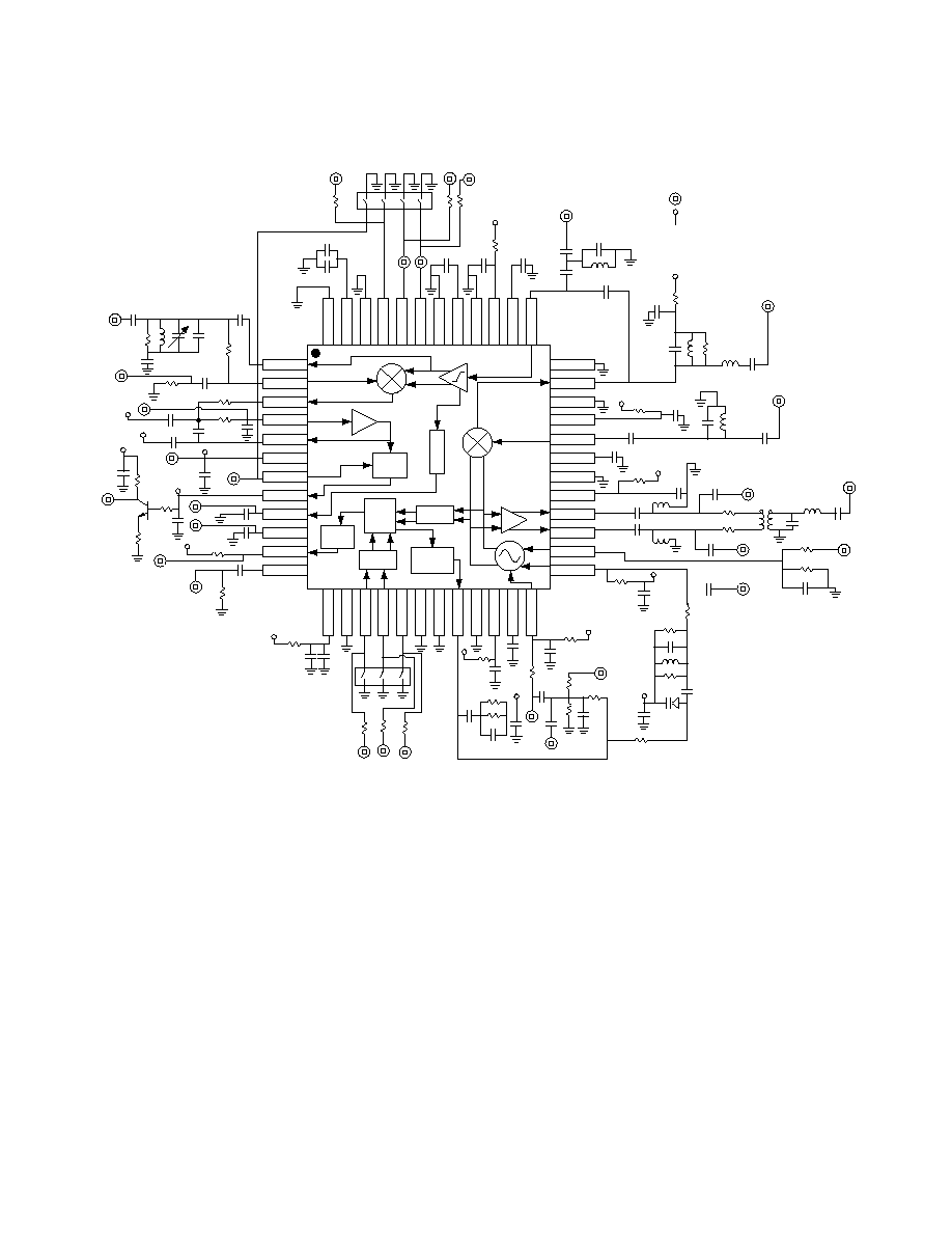
- 1. HPMX-5002 Test Board Schematic Diagram.
- 2. HPMX-5002 Detailed Block Diagram.
- 3. Typical HPMX-5002 Application with HPMX-5001 T/R Chip.
- 4. HPMX-5002 Internal and Equivalent Circuits, Pins 1-5.
- 5. HPMX-5002 Internal and Equivalent Circuits, Pins 8, 9, 11, 24, 25, 27, and 28.
- 6. HPMX-5002 Internal and Equivalent Circuits, Pins 32, 35, and 37.
- List of Tables
- 1. HPMX-5002 Mode Control
- 2. HPMX-5002 PLL Divider Programming
- Features
- Applications
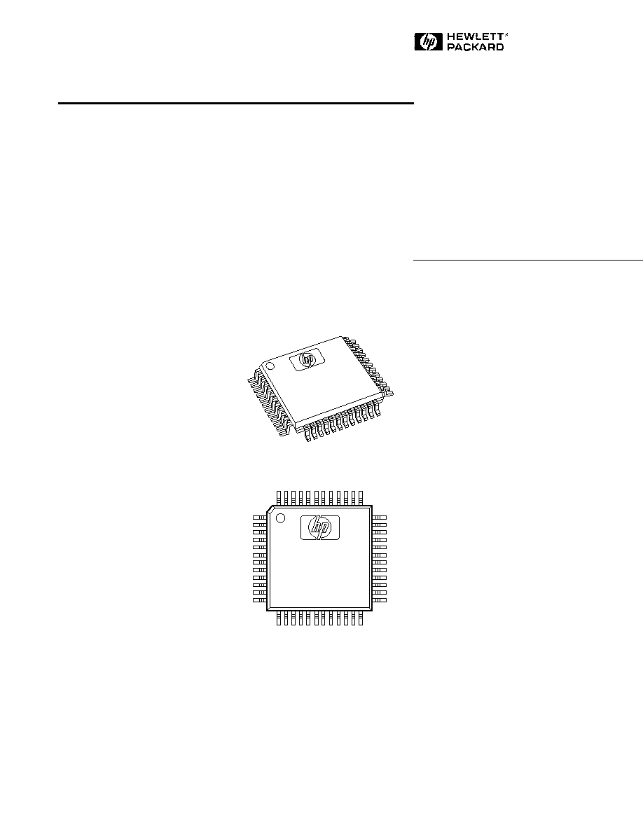
- Plastic TQFP-48 Package
- Pin Configuration
- Description
- HPMX-5002 Functional Block Diagram
- HPMX-5002 Absolute Maximum Ratings [1]
- HPMX-5002 Guaranteed Electrical Specifications
- HPMX-5002 Summary Characterization Information
- HPMX-5002 Pin Description
- Functional Description
- Detailed Circuit Description
- Tape Dimensions and Product Orientation for Outline TQFP-48
7-105
IF Modulator/Demodulator IC
Technical Data
Features
∑ Use with HPMX-5001
Up/Down Converter Chip
for DECT Telephone
Applications
∑ 2.7≠ 5.5 V Single Supply
Voltage
∑ >75 dB RSSI Range
∑ Internal Data Slicer
∑ On-chip LO Generation,
Including VCO, Prescalers
and Phase/ Frequency
Detector
∑ Flexible Chip Biasing,
Including Standby Mode
∑ Supports Reference Crystal
Frequencies of 9, 12, and 16
Times the DECT Bit Rate
(1.152 MHz)
∑ IF Input Frequency Range
up to 250 MHz
∑ TQFP-48 Surface Mount
Package
Applications
∑ DECT, Unlicensed PCS and
ISM Band Handsets,
Basestations and Wireless
LANs
HPMX-5002
Description
The Hewlett-Packard HPMX-5002
IF Modulator/Demodulator
provides all of the active compo-
nents necessary for the demodula-
tion of a downconverted DECT
signal. Designed specifically for
DECT, the HPMX-5002 contains a
down-conversion mixer (to a 2nd
IF), limiting amplifier chain,
discriminator/data slicer, lock
detector, and RSSI circuits. The
LO2 generation is also included
on-chip, via a VCO, dividers, and
phase/frequency detector. The
divide ratios are programmable to
support reference frequencies of
either 9, 12, or 16 times the DECT
bit rate of 1.152 MHz allowing the
use of common, low cost crystals.
The LO2 VCO can also be utilized in
transmit mode by directly modulat-
ing the external VCO tank. An AGC
loop in the buffered VCO output
suppresses harmonics and reduces
signal level variability.
The HPMX-5002 is designed to meet
the size and power demands of
portable applications. Battery cell
count and cost are reduced due to
the 2.7 V minimum supply voltage.
The TQFP-48 package, combined
with the high level of integration,
means smaller footprints and fewer
components. Flexible chip biasing
takes full advantage of the power
savings inherent in time-duplexed
systems such as DECT.
Plastic TQFP-48 Package
HPMX
≠ 5002
9433
6435
019
Pin Configuration
HPMX ≠ 5002
9433
6435
019
24
37
13
48
25
36
12
1
5965-9106E
7-106
Figure 1. HPMX-5002 Test Board Schematic Diagram.
4
3
2
1
IFOP1
1
48
37
36
R
S
S
I
DATA
SLICER
9/12/16
90/216
CHARGE
PUMP
LOCK
DET
25
24
13
12
5
0.1
µ
0.01
µ
0.01
µ
6
100 k
7
8
NC
BGR
NC
RX
PLL
XLO
VSUB
DC1B
VEE2
VCC2
DC1A
1F1P1
VCC3
VEE3
D1V1
D1V2
D1V3
NC
NC
PFD
VEE4
VCC4
AGC
VCOA
DMOD
DMODOP
BUF1
BUF2
TCNT
TCSET
DATOP
RSS1
LKFIL
LKDET
REF
NC
IF1
VEE1
VCC1
IP1
IPDC
VEE5
VCC5
OSCOPB
OSCOP
VCOADJ
VCOB
100 k
100 k
0.01
µ
0.01
µ
100 p
10 p
= connector
= terminal
DC post
2.7
µ
H
3.9
µ
H
3.9
µ
H
0.01
µ
100 p
1 p
10 p
1 p
22 p
68 p
0.01
µ
0.01
µ
0.01
µ
0.01
µ
100 nH
270 nH
270 nH
0
0
10
51.1
1 k
0
1.2 k
10
8.2 p
8.2 p
20 k
220 nH
1000 p
0.01
µ
0.01
µ
0
0
20 k
Freq.
Det.
8.2 p
0.01
µ
0
3.9 p
0.01
µ
330 p
3.3 k
4.7 k
1000 p
10
120 n
10 k
10 k
1 k
22 p
0
0.01
µ
0.01
µ
0.01
µ
4400 p
0.01
µ
0.01
µ
0.01
µ
3
1000 p
1 k
0
0.01
µ
2
1
4
5
6
1000 p
49.9
10
0.01
µ
0.01
µ
68 p
3.9 p
22 p
15
µ
H
1000 p
3 to 10 p
0.01
µ
0.01
µ
0.01
µ
0.01
µ
1000 p
10 p
1000 p
22 p
1 k
1 k
6 k
0.01
µ
20 k
0
4.7 k
4.7 k
0
49.9
7-107
HPMX-5002 Functional Block Diagram
IP1
IFIP1
IFOP1
BUF1
BUF2
TCSET
DATA
SLICER
9/12/16
DATAOP
RSSI
DIV2
DIV1
REF
BGR
BIAS
CONTROL
DMOD
DMODOP
90/216
CHARGE
PUMP
FREQ.
DET.
LOCK
DET.
LKDET
PFD
DIV3
VCOA
VCOB
VCOADJ
PLL
XLO
RX
RSSI
IF1
OSCOP
OSCOPB
HPMX-5002 Absolute Maximum Ratings
[1]
Symbol
Parameter
Units
Min.
Max.
V
CC
Supply Voltage
V
-0.2
7.5
Voltage at any Pin
[4]
V
-0.2
V
CC
+ 0.2
P
diss
Power Dissipation
[2,3]
mW
200
Junction Temperature
∞
C
+110
T
STG
Storage Temperature
∞
C
-55
+125
Thermal Resistance
[2]
:
jc
= 80
∞
C/W
Notes:
1. Operation of this device in excess
of any of these parameters may
cause permanent damage.
2. T
case
= 25
∞
C
3. Derate at 10 mW/
∞
C for T
case
> 90
∞
C
4. Except CMOS logic inputs, see
Summary Characterization
Information Table.
HPMX-5002 Guaranteed Electrical Specifications
Unless otherwise noted, all parameters are guaranteed under the following conditions: 2.7 V < V
CC
< 5.5 V.
Test results are based upon use of networks shown in test diagram (see Figure 1). f
in
= 110.592 MHz.
Typical values are for V
CCX
= 3.0 V, T
A
= 25
∞
C.
Symbol
Parameters and Test Conditions
Units
Min.
Typ.
Max.
I
ccx
Total V
ccx
supply current
RX mode
mA
21
27
(PLL locked)
(PLL locked)
PLL mode
mA
16
20
TX "flywheel" mode
mA
9
11.5
Standby mode
µ
A
100
Charge pump current
high current mode
µ
A
400
550
1000
Charge pump current
low current mode
µ
A
30
50
100
GIF1
Mixer power gain from
input matched to 50
dB
5
8
IP1 to IF1, external load
impedance of 600
VDATOP
Data slicer output level
Logic `0'
V
0.3
VDATOP
Data slicer output level
Logic `1'
V
V
ccx
- 0.3
7-108
HPMX-5002 Summary Characterization Information
Typical values measured on test board shown in Figure 1 at V
ccx
= 3.0 V, T
A
= 25
∞
C,
f
in
= 110.592 MHz, f
LO2
= 103.68 MHz, unless otherwise noted.
Symbol
Parameters and Test Conditions
Units
Typ.
V
IH
CMOS input high voltage (can be pulled up as high as V
cc
+7V)
V
V
cc
-0.8
V
IL
CMOS input low voltage
V
1.0
I
IH
CMOS input high current
µ
A
< 50
I
IL
CMOS input low current
µ
A
> - 50
Mode switching time
µ
S
< 1
P
1 dB
Mixer input 1 dB compression point
matched to 50
source
dBm
-23
I
IP3
Mixer input IP3
matched to 50
source
dBm
-17
NF
IF1
Mixer SSB noise figure
input matched to 50
dB
12
(see test diagram Fig. 1)
source, 600
load at output
Z
inIP1
Mixer input impedance
50 MHz < f
in
< 250 MHz
100
RSSI dynamic range
Note 1
dB
75
(for signal input at IFIP1; RSSI output measured with 6 bit ADC)
RSSI voltage change
Note 1
mV/dB
17
RSSI output voltage. V
ccx
= 3 V,
2 IF limiter input level:
V
RSSI
is monotonic
- 90 dBm
V
0.88
-50 dBm
1.48
-20 dBm
2.04
Z
outRSSI
RSSI output impedance
k
30
IF2f
3 dB
IF2 limiter bandwidth
MHz
45
A
VIF2
IF2 limiter voltage gain
Prior to limiting, Note 2
dB
57
Z
inIFIP1
IF2 limiter input impedance at pin IFIP1
Note 2
600
V
outLO2
LO2 output buffer differential amplitude
> 1.5 k
differential load,
mVp-p
335
(between OSCOP and OSCOPB)
f
vco
=103.68 MHz, V
CC
= 3 V
Bit slicer time constant ratio
TCSET =0 vs. TCSET = 1
80:1
LO2 VCO output buffer noise floor
tank circuit Q = 35
dBc/Hz
-142
(@ 4 MHz offset)
PLL charge pump leakage current
pA
<100
ILKDET
Lock detector current sink
Logic `0' (unlocked)
mA
1.1
Notes:
1: RSSI signal is monotonic over stated dynamic range, but not necessarily linear. Voltage change is
defined in the linear region of the transfer curve.
2: IF2 frequency in the range 1 MHz < f < 45 MHz, with 10 nF capacitors from DC1A and DC1B to
ground.
7-109
HPMX-5002 Pin Description
No.
Mnemonic
I/O Type
Description
1
IFOP1
Analog O/P
Output of IF amplifier, feeds quadrature network for discriminator
2
DMOD
Analog I/P
Input to discriminator mixer, driven by output of quadrature network
3
DMODOP
Analog O/P
Output of discriminator mixer, drives external low-pass data filter
4
BUF1
Analog I/P
Noninverting input of buffer amplifier that drives the data slicer
5
BUF2
Analog O/P
Output of buffer amplifer that drives the data slicer
6
TCNT
Analog DC
External capacitor connection which sets time constant for data slicer
7
TCSET
CMOS I/P
Data slicer time constant select
8
DATOP
CMOS O/P
Output bit stream from data slicer
9
RSSI
Analog O/P
Receive Signal Strength Indicator output
10
LKFIL
Analog DC
External capacitor connection which sets time constant for lock detector
11
LKDET
CMOS O/P
Indicates that LO2 PLL is in lock status
12
REF
Analog I/P
Reference signal for LO2 PLL
13
VCC3
DC Supply
PLL supply voltage
14
VEE3
Ground
PLL ground
15
DIV1
CMOS I/P
Controls divide ratio for reference frequency input to the LO2 PLL
16
DIV2
CMOS I/P
Controls divide ratio for reference frequency input to the LO2 PLL
17
DIV3
CMOS I/P
Controls divide ratio for VCO frequency input to the LO2 PLL
20
PFD
Analog O/P
LO2 PLL phase/frequency detector charge pump output
21
VEE4
Ground
LO2 VCO ground
22
VCC4
DC Supply
LO2 VCO supply voltage
23
AGC
Analog DC
External capacitor connection to compensate LO2 VCO AGC loop
24
VCOA
Analog I/P
VCO tank force line
25
VCOB
Analog O/P
VCO tank sense line
26
VCOADJ
Analog I/P
Controls amplitude of buffered LO2 VCO output
27
OSCOP
Analog O/P
Buffered LO2 output (+)
28
OSCOPB
Analog O/P
Buffered LO2 output (-)
29
VCC5
DC Supply
1st IF supply voltage
30
VEE5
Ground
1st IF ground
31
IPDC
Analog DC
External capacitor connection for decoupling 1st IF bias point
32
IP1
Analog I/P
1st IF input signal
33
VCC1
DC Supply
IF limiting amplifier supply voltage
34
VEE1
Ground
IF limiting amplifier ground
35
IF1
Analog O/P
Downconverted signal from front-end mixer, drives external filter
(hi-Z output, open collector)
37
IFIP1
Analog I/P
Input to IF limiting amplifier, driven by external filter
(600
impedance, internally set)
38
DC1A
Analog DC
External capacitor connection for decoupling IF limiting amplifier
39
VCC2
DC Supply
IF limiting amplifier supply voltage
40
VEE2
Ground
IF limiting amplifier ground