 | ÐлекÑÑоннÑй компоненÑ: QCPM-9804 | СкаÑаÑÑ:  PDF PDF  ZIP ZIP |
1QX5A Data Sheet (for sampling tour)
QCPM-9804 Rev. G Feb-8-2000 Preliminary
Specification is subject to change without prior notification
PCS/CDMA/AMPS Dual-Band Tri-Mode
Power Amplifier Module
QCPM-9804
_____________________
Features
·
·
·
·
Operating frequency:
PCS: 1850 - 1910 MHz
AMPS: 824 - 849 MHz
CDMA: 824 - 829 MHz
·
Typical Output Power @
3.4V:
PCS : 28.5 dBm
AMPS: 32.5 dBm
CDMA: 28.5 dBm
·
Internal 50 ohm matching
networks for both RF
IN/OUT
·
3.4 - 4.2 V operation
(reduced
performance at 3V)
·
·
·
·
Dynamic bias controls
optimize PAE at low output
power for PCS and cellular
CDMA mode
·
·
·
·
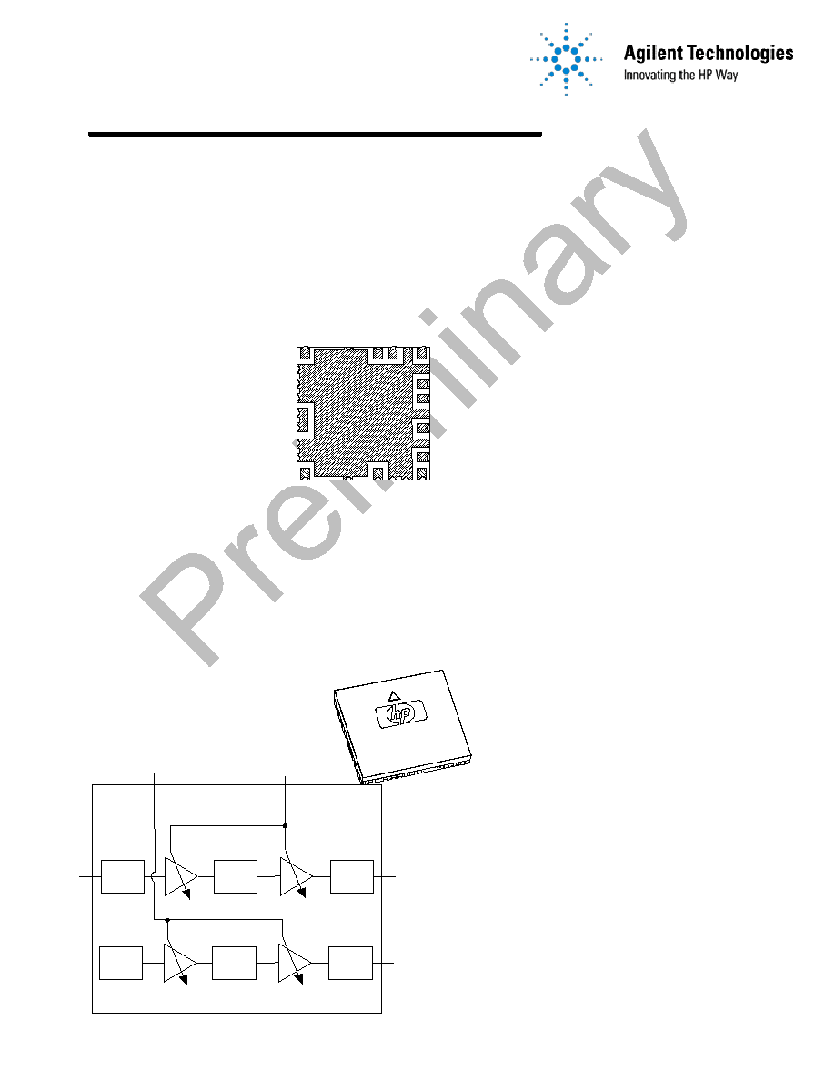
11.5 mm x 11.5 mm SMT RF
MultiPak
Applications
·
·
·
·
Dual Band CDMA handsets
·
·
·
·
Wireless Data terminals
·
WLL
·
Driver for Base station
Small SMT Multipak
General Description
The Dual-Band Tri-Mode Power
Amplifier Module (PAM) offers a
highly integrated solution for
CDMA dual-band tri-mode
handsets. The integrated solution
leads to improvements in cost,
size, performance, and reliability.
This PAM also offers several
features that will make handset
design more flexible and robust.
The module contains two power
amplifiers (PCS and Cellular PAs),
two driver amplifiers with power
control and bias circuits.
The cellular power amplifiers
provide: 32.5 dBm Pout and 47%
Power Added Efficiency (PAE) at
3.4 V in AMPS mode, and 28.5
dBm Pout and 29% PAE at 3.4 V in
cellular CDMA mode. While the
PCS power amplifier achieves 28.5
dBm Pout and 28 % PAE at 3.4V in
PCS mode. The PAM is designed
with dynamic bias control to
optimize the PAE at low output
power in PCS and cellular CDMA
mode to maximize the system talk
time.
The surface mount RF MultiPak
insures cost, size, and high volume
manufacturing advantages over
other traditional approaches.
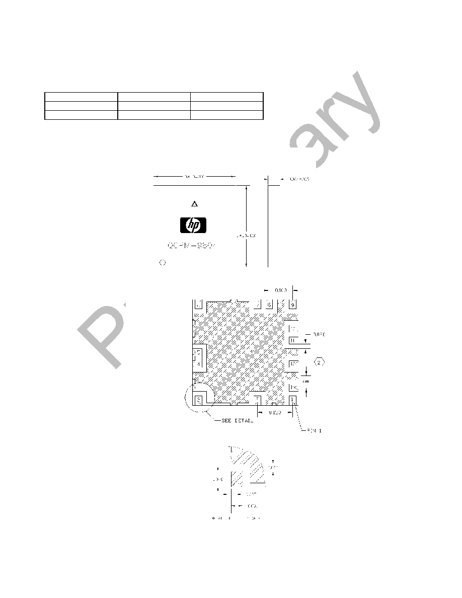
Package Pin Configuration
(Back side)
Functional Block Diagram
6
7 8
9
10
11
12
13
1
2
3
4
5
14
QCPM
-9804
matching
network
matching
network
matching
network
matching
network
matching
network
matching
network
CELLULAR
PA IN
PCS CDMA
IN
PCS CDMA
OUT
CELLULAR
PA OUT
AMPS_Vc
CDMA_Vc
QCPM-9804 Rev. G Feb-8-2000 Preliminary
Specification is subject to change without prior notification
2
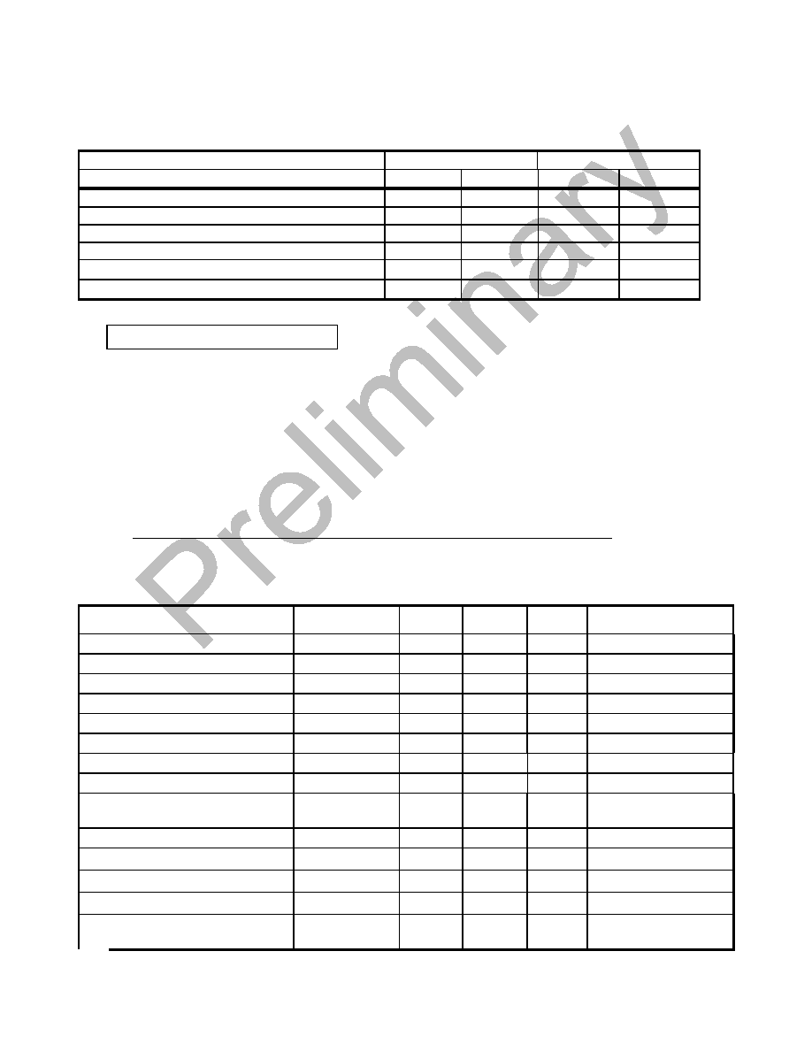
QCPM-9804 Absolute Maximum Ratings
1
Cellular
PCS
Parameter
Min.
Max.
Min.
Max.
Vcc supply voltage
4.5 V
4.5 V
Power Dissipation2,3
2.5 W
2.5 W
Bias Current
1.5 A
1.5 A
Amplifier Input RF Power
10 dBm
10 dBm
Junction temperature
+150
°
C
+150
°
C
Storage temperature (case temperature)
-40
°
C
+120
°
C
-40
°
C
+120
°
C
Thermal Resistance
2
jc = X
°
/W
Notes:
1. Operation of this device in excess of any of these limits may
cause permanent damage.
2. Tcase = 25
°
C
3.
Derate at X mW/
°
C for Tcase.>85
°
C
Recommended operating range of Vcc = 3.4 to 4.2 V, Ta = - 30 to + 85
°
C (reduced performance at 3.0 V and
110
°
C)
QCPM-9804 Standard Test Conditions
All test are done in 50
system at 25
°
C , unless noted otherwise.
V
CC
= 3.4V
ACPR
Channel
Power
in
the
MHz
band
Power in a
KHz
band
MHz away
from
the center of
the channel
=
±
12288
30
1 25
.
@ .
QCPM-9804 Summary Characterization Information
Parameter
Units
Min
Typ
Max Comments
PCS Mode
Frequency Range
MHz
1850
1910
Gain (P
out
= 28.5 dBm)
dB
22
24
Vc=2.5V
Gain (P
out
= 16 dBm)
dB
19
21
Vc=1.8V
Output Power
dBm
28
28.5
Power Added Efficiency
P
out
= 28.5 dBm
%
TBA
28
P
out
= 16 dBm
%
TBA
6
Input VSWR (P
out
= 28.5
dBm)
2.0:1
Input VSWR (P
out
= 16 dBm)
2.5:1
Power Down Current
µ
A
40
ACPR @
±
1.25 MHz offset
dBc/30kHz
-45
-46
ACPR @
±
2.25 MHz offset
dBc/30kHz
-58
Noise Power @ 80 MHz
offset in 1930-1990 MHz )
dBm/Hz
-139
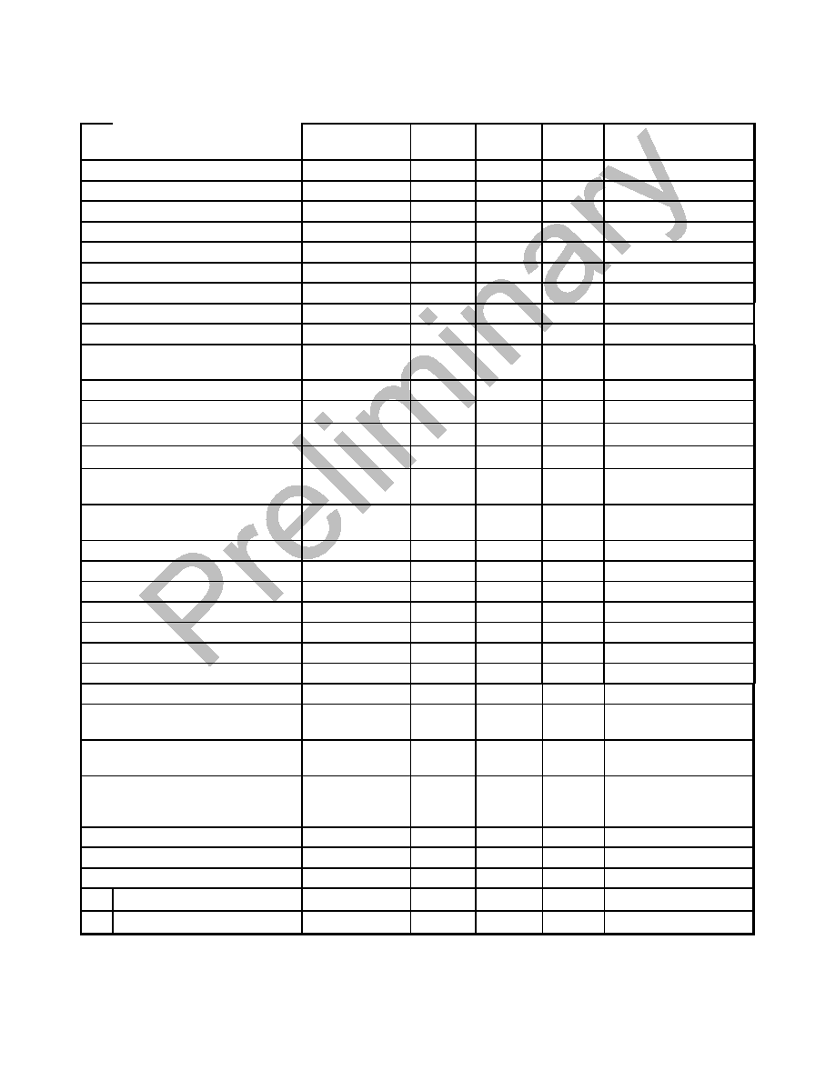
QCPM-9804 Rev. G Feb-8-2000 Preliminary
Specification is subject to change without prior notification
3
Stability (Spurious): Load
VSWR 5:1
dBc
55
All phases
Harmonics: 2Fo, 3Fo
dBc
-30
CDMA mode
Frequency Range
MHz
824
849
Gain (P
out
= 28.5 dBm)
dB
27
29
Vc=2.15V
Gain (P
out
= 16 dBm)
dB
23
25
Vc=1.8V
Output Power
dBm
28.5
Power Added Efficiency
P
out
= 28.5 dBm
%
TBA
29
P
out
= 16 dBm
%
TBA
6
Input VSWR (P
out
= 28.5
dBm)
2.0:1
Input VSWR (P
out
= 16 dBm)
2.5:1
Power Down Current
µ
A
40
ACPR @
±
0.885 MHz offset
dBc/30kHz
-45
-47
ACPR @
±
1.98 MHz offset
dBc/30kHz
-57
Noise Power @ 45 MHz
offset in 869 - 894 MHz
dBm/Hz
-140
Stability (Spurious): Load
VSWR 4:1
dBc
55
All phases
Harmonics: 2Fo, 3Fo
dBc
-30
AMPS mode
Frequency Range
MHz
824
849
Output Power (P
in
= 7.5
dBm)
dBm
32.5
Power Added Efficiency (P
out
= 32.5 dBm)
%
TBA
47
Vc=2.15V
Noise Power @ 45 MHz
offset in RX band (869-
894MHz)
dBm/Hz
-136
Harmonics: 2Fo, 3Fo
dBc
-30
Input VSWR
2:1
Switching Time
DC ON/OFF
µ
s
40
RF ON/OFF
µ
s
6
QCPM-9804 Rev. G Feb-8-2000 Preliminary
Specification is subject to change without prior notification
4
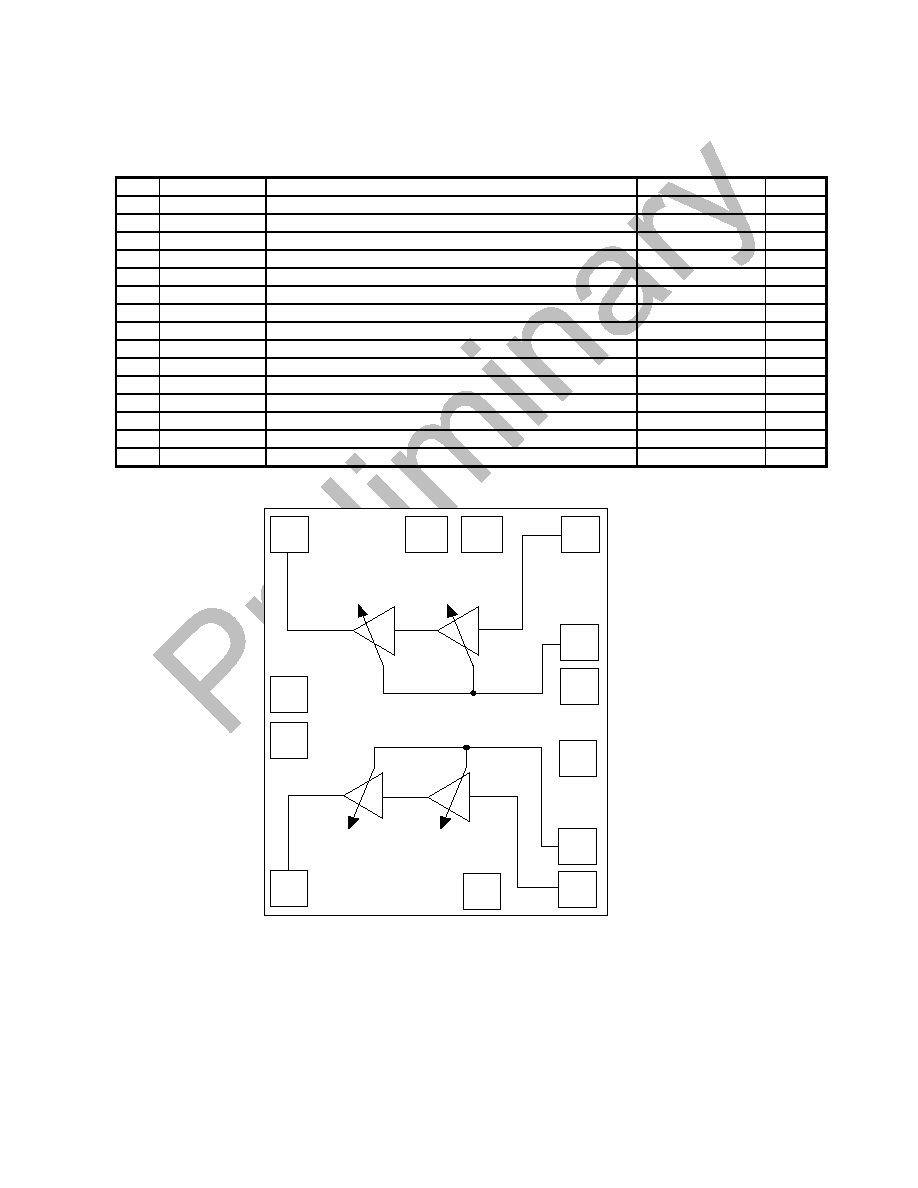
QCPM-9804 Pin Description Table
No.
Mnemonic
Description
Typical Signal
Notes
1
CDMA_IN_A
Input RF for PCS CDMA
RF input
2
Not connect
3
CDMA OUT
RF PCS CDMA output
RF Output
4
CDMA Vcc
Supply voltage for CDMA
DC
5
AMPS Vcc
Supply voltage for AMPS and cellular CDMA
DC
6
AMPS OUT
RF AMPS and cellular CDMA output
RF Output
7
Not connect
8
Not connect
9
AMPS IN
RF AMPS and cellular CDMA input
RF
10
AMPS_Vc
Bias control for AMPS and cellular CDMA PA
11
Vcc_IC
Supply voltage for control and driver
DC
12
Not connect
13
CDMA_Vc
Bias control for PCS CDMA PA
14
GND
Ground plane (back of the module)
6
2
5
4
3
9
AMPS
OUT
AMPS
IN
NC
CDMA
IN_A
CDMA
OUT
Vcc
CDMA
Vcc
AMPS
AMPS
Vc
Vcc
IC
CDMA
Vc
10
11
12
13
1
NC
8
7
NC
NC
Figure 1 Internal block diagram with pinout (back side)
QCPM-9804 Rev. G Feb-8-2000 Preliminary
Specification is subject to change without prior notification
5
Part Number Ordering Information
Part Number
No. of Devices
Container
QCPM-9804
Package Dimensions Small MultiPak-16 Package (in inches)
Document Outline