
comtech aha corporation
1126 Alturas Drive
Moscow ID 83843
tel: 208.892.5600
fax: 208.892.5601
www.aha.com
A subsidiary of Comtech Telecommunications Corporation
PS4540evb_0405
Product Specification
AHA4540-EVB
Turbo Product Code Evaluation Board
This product is covered by a Turbo Code Patent License from France Telecom - TDF - Groupe des ecoles des telecommunications.
This product is covered under multiple patents held or licensed by Comtech AHA Corporation.

comtech aha corporation
PS4540evb_0405
A subsidiary of Comtech Telecommunications Corporation
i
Table of Contents
1.0 Introduction . . . . . . . . . . . . . . . . . . . . . . . . . . . . . . . . . . . . . . . . . . . . . . . . . . . . . . . . . . . . . . . . . . . . . . . . . . . . . 1
1.1 Conventions, Notations and Definitions. . . . . . . . . . . . . . . . . . . . . . . . . . . . . . . . . . . . . . . . . . . . . . . . . . . . . 1
1.2 Features . . . . . . . . . . . . . . . . . . . . . . . . . . . . . . . . . . . . . . . . . . . . . . . . . . . . . . . . . . . . . . . . . . . . . . . . . . . . 2
1.3 System Requirements . . . . . . . . . . . . . . . . . . . . . . . . . . . . . . . . . . . . . . . . . . . . . . . . . . . . . . . . . . . . . . . . . . 2
1.4 Modes . . . . . . . . . . . . . . . . . . . . . . . . . . . . . . . . . . . . . . . . . . . . . . . . . . . . . . . . . . . . . . . . . . . . . . . . . . . . . . 2
2.0 Functional Overview . . . . . . . . . . . . . . . . . . . . . . . . . . . . . . . . . . . . . . . . . . . . . . . . . . . . . . . . . . . . . . . . . . . . . . 3
2.1 Encoding Operation. . . . . . . . . . . . . . . . . . . . . . . . . . . . . . . . . . . . . . . . . . . . . . . . . . . . . . . . . . . . . . . . . . . . 3
2.1.1
Encode Data Input . . . . . . . . . . . . . . . . . . . . . . . . . . . . . . . . . . . . . . . . . . . . . . . . . . . . . . . . . . . . . . 3
2.1.2
Encode Data Output . . . . . . . . . . . . . . . . . . . . . . . . . . . . . . . . . . . . . . . . . . . . . . . . . . . . . . . . . . . . . 4
2.2 Decoding Operation. . . . . . . . . . . . . . . . . . . . . . . . . . . . . . . . . . . . . . . . . . . . . . . . . . . . . . . . . . . . . . . . . . . . 4
2.2.1
Decode Data Input . . . . . . . . . . . . . . . . . . . . . . . . . . . . . . . . . . . . . . . . . . . . . . . . . . . . . . . . . . . . . . 4
2.2.2
Decode Data Output. . . . . . . . . . . . . . . . . . . . . . . . . . . . . . . . . . . . . . . . . . . . . . . . . . . . . . . . . . . . . 4
2.3 Clock Sources . . . . . . . . . . . . . . . . . . . . . . . . . . . . . . . . . . . . . . . . . . . . . . . . . . . . . . . . . . . . . . . . . . . . . . . . 4
2.3.1
Crystal Oscillators . . . . . . . . . . . . . . . . . . . . . . . . . . . . . . . . . . . . . . . . . . . . . . . . . . . . . . . . . . . . . . 4
2.3.2
Frequency Synthesizers . . . . . . . . . . . . . . . . . . . . . . . . . . . . . . . . . . . . . . . . . . . . . . . . . . . . . . . . . . 4
2.4 Synchronization Support . . . . . . . . . . . . . . . . . . . . . . . . . . . . . . . . . . . . . . . . . . . . . . . . . . . . . . . . . . . . . . . . 5
2.4.1
Led Status Definitions (D1-D8). . . . . . . . . . . . . . . . . . . . . . . . . . . . . . . . . . . . . . . . . . . . . . . . . . . . . 5
2.4.2
Switch Definitions . . . . . . . . . . . . . . . . . . . . . . . . . . . . . . . . . . . . . . . . . . . . . . . . . . . . . . . . . . . . . . . 5
2.4.3
Jumper Clock Configuration (JP7) . . . . . . . . . . . . . . . . . . . . . . . . . . . . . . . . . . . . . . . . . . . . . . . . . . 5
2.4.4
Jumper Clock Configuration (JP8) . . . . . . . . . . . . . . . . . . . . . . . . . . . . . . . . . . . . . . . . . . . . . . . . . . 5
2.5 Loopback - Test 1 . . . . . . . . . . . . . . . . . . . . . . . . . . . . . . . . . . . . . . . . . . . . . . . . . . . . . . . . . . . . . . . . . . . . . 5
2.6 Loopback - Test 2 . . . . . . . . . . . . . . . . . . . . . . . . . . . . . . . . . . . . . . . . . . . . . . . . . . . . . . . . . . . . . . . . . . . . . 6
2.7 Loopback - Test 3 . . . . . . . . . . . . . . . . . . . . . . . . . . . . . . . . . . . . . . . . . . . . . . . . . . . . . . . . . . . . . . . . . . . . . 6
2.8 Loopback Test 4. . . . . . . . . . . . . . . . . . . . . . . . . . . . . . . . . . . . . . . . . . . . . . . . . . . . . . . . . . . . . . . . . . . . . . . 6
2.9 Loopback - Test 5 . . . . . . . . . . . . . . . . . . . . . . . . . . . . . . . . . . . . . . . . . . . . . . . . . . . . . . . . . . . . . . . . . . . . . 6
2.10 EVB configuration for Mode 1 . . . . . . . . . . . . . . . . . . . . . . . . . . . . . . . . . . . . . . . . . . . . . . . . . . . . . . . . . . . . 7
2.11 Mode 1 Script Writing . . . . . . . . . . . . . . . . . . . . . . . . . . . . . . . . . . . . . . . . . . . . . . . . . . . . . . . . . . . . . . . . . . 7
2.12 Software Installation . . . . . . . . . . . . . . . . . . . . . . . . . . . . . . . . . . . . . . . . . . . . . . . . . . . . . . . . . . . . . . . . . . . 7
2.13 Quick Start. . . . . . . . . . . . . . . . . . . . . . . . . . . . . . . . . . . . . . . . . . . . . . . . . . . . . . . . . . . . . . . . . . . . . . . . . . . 7
3.0 Hardware Description . . . . . . . . . . . . . . . . . . . . . . . . . . . . . . . . . . . . . . . . . . . . . . . . . . . . . . . . . . . . . . . . . . . . . 8
4.0 FPGA Controller Toplevel Description . . . . . . . . . . . . . . . . . . . . . . . . . . . . . . . . . . . . . . . . . . . . . . . . . . . . . . . . 9
5.0 AHA4540-EVB Communication Software . . . . . . . . . . . . . . . . . . . . . . . . . . . . . . . . . . . . . . . . . . . . . . . . . . . . 10
5.1 Operation of AHAESB Software . . . . . . . . . . . . . . . . . . . . . . . . . . . . . . . . . . . . . . . . . . . . . . . . . . . . . . . . . 10
5.1.1
Connect Button. . . . . . . . . . . . . . . . . . . . . . . . . . . . . . . . . . . . . . . . . . . . . . . . . . . . . . . . . . . . . . . . 10
5.1.2
Configure Button. . . . . . . . . . . . . . . . . . . . . . . . . . . . . . . . . . . . . . . . . . . . . . . . . . . . . . . . . . . . . . . 10
5.1.3
Interactive Mode Window . . . . . . . . . . . . . . . . . . . . . . . . . . . . . . . . . . . . . . . . . . . . . . . . . . . . . . . . 10
5.1.4
Log Window . . . . . . . . . . . . . . . . . . . . . . . . . . . . . . . . . . . . . . . . . . . . . . . . . . . . . . . . . . . . . . . . . . 10
5.1.5
Reset Status . . . . . . . . . . . . . . . . . . . . . . . . . . . . . . . . . . . . . . . . . . . . . . . . . . . . . . . . . . . . . . . . . . 10
5.1.6
User Test Modes. . . . . . . . . . . . . . . . . . . . . . . . . . . . . . . . . . . . . . . . . . . . . . . . . . . . . . . . . . . . . . . 10
5.1.7
Test Modes . . . . . . . . . . . . . . . . . . . . . . . . . . . . . . . . . . . . . . . . . . . . . . . . . . . . . . . . . . . . . . . . . . . 10
5.1.8
AHAESB Script Syntax. . . . . . . . . . . . . . . . . . . . . . . . . . . . . . . . . . . . . . . . . . . . . . . . . . . . . . . . . . 10
5.2 ESB Status . . . . . . . . . . . . . . . . . . . . . . . . . . . . . . . . . . . . . . . . . . . . . . . . . . . . . . . . . . . . . . . . . . . . . . . . . 10
6.0 REFERENCE GUIDE TO PROGRAMMING EVB REGISTERS . . . . . . . . . . . . . . . . . . . . . . . . . . . . . . . . . . . . . 11
6.1 Register Description . . . . . . . . . . . . . . . . . . . . . . . . . . . . . . . . . . . . . . . . . . . . . . . . . . . . . . . . . . . . . . . . . . 12
7.0 Register Programming . . . . . . . . . . . . . . . . . . . . . . . . . . . . . . . . . . . . . . . . . . . . . . . . . . . . . . . . . . . . . . . . . . . 15
7.1 AHA4540 Registers . . . . . . . . . . . . . . . . . . . . . . . . . . . . . . . . . . . . . . . . . . . . . . . . . . . . . . . . . . . . . . . . . . . 15
7.2 Frequency Synthesizers . . . . . . . . . . . . . . . . . . . . . . . . . . . . . . . . . . . . . . . . . . . . . . . . . . . . . . . . . . . . . . . 15
7.3 AHA4540-EVB FPGA Registers . . . . . . . . . . . . . . . . . . . . . . . . . . . . . . . . . . . . . . . . . . . . . . . . . . . . . . . . . 15
8.0 Signals In/Out of EVB . . . . . . . . . . . . . . . . . . . . . . . . . . . . . . . . . . . . . . . . . . . . . . . . . . . . . . . . . . . . . . . . . . . . 16
8.1 EVB Main Board . . . . . . . . . . . . . . . . . . . . . . . . . . . . . . . . . . . . . . . . . . . . . . . . . . . . . . . . . . . . . . . . . . . . . 16
9.0 Electrical Specifications . . . . . . . . . . . . . . . . . . . . . . . . . . . . . . . . . . . . . . . . . . . . . . . . . . . . . . . . . . . . . . . . . . 16
9.1 Board Power . . . . . . . . . . . . . . . . . . . . . . . . . . . . . . . . . . . . . . . . . . . . . . . . . . . . . . . . . . . . . . . . . . . . . . . . 16

comtech aha corporation
ii
A subsidiary of Comtech Telecommunications Corporation
PS4540evb_0405
9.2 Signal Requirements . . . . . . . . . . . . . . . . . . . . . . . . . . . . . . . . . . . . . . . . . . . . . . . . . . . . . . . . . . . . . . . . . . 16
10.0 Timing Specifications . . . . . . . . . . . . . . . . . . . . . . . . . . . . . . . . . . . . . . . . . . . . . . . . . . . . . . . . . . . . . . . . . . . . 17
11.0 Board Dimensions . . . . . . . . . . . . . . . . . . . . . . . . . . . . . . . . . . . . . . . . . . . . . . . . . . . . . . . . . . . . . . . . . . . . . . . 17
12.0 Ordering Information . . . . . . . . . . . . . . . . . . . . . . . . . . . . . . . . . . . . . . . . . . . . . . . . . . . . . . . . . . . . . . . . . . . . . 17
13.0 About AHA . . . . . . . . . . . . . . . . . . . . . . . . . . . . . . . . . . . . . . . . . . . . . . . . . . . . . . . . . . . . . . . . . . . . . . . . . . . . . 18
Appendix A: Board Schematics . . . . . . . . . . . . . . . . . . . . . . . . . . . . . . . . . . . . . . . . . . . . . . . . . . . . . . . . . . . . . . . . 19

comtech aha corporation
PS4540evb_0405
A subsidiary of Comtech Telecommunications Corporation
iii
List of Figures
Figure 1: AHA4540-EVB Photo . . . . . . . . . . . . . . . . . . . . . . . . . . . . . . . . . . . . . . . . . . . . . . . . . . . . . . . . . . . . . . . . . .1
Figure 2: AHA4540-EVB Block Diagram . . . . . . . . . . . . . . . . . . . . . . . . . . . . . . . . . . . . . . . . . . . . . . . . . . . . . . . . . . .3
Figure 3: Encode/Decode Loopback - Test 1 Datapath . . . . . . . . . . . . . . . . . . . . . . . . . . . . . . . . . . . . . . . . . . . . . . .6
Figure 4: AHA4540-EVB Major Component Diagram . . . . . . . . . . . . . . . . . . . . . . . . . . . . . . . . . . . . . . . . . . . . . . . . .8
Figure 5: FPGA Block Diagram . . . . . . . . . . . . . . . . . . . . . . . . . . . . . . . . . . . . . . . . . . . . . . . . . . . . . . . . . . . . . . . . . .9
Figure 6: Data Input Timings . . . . . . . . . . . . . . . . . . . . . . . . . . . . . . . . . . . . . . . . . . . . . . . . . . . . . . . . . . . . . . . . . . .17
Figure 7: Data Output Timings . . . . . . . . . . . . . . . . . . . . . . . . . . . . . . . . . . . . . . . . . . . . . . . . . . . . . . . . . . . . . . . . .17

comtech aha corporation
iv
A subsidiary of Comtech Telecommunications Corporation
PS4540evb_0405
List of Tables
Table 1:
LED Definition . . . . . . . . . . . . . . . . . . . . . . . . . . . . . . . . . . . . . . . . . . . . . . . . . . . . . . . . . . . . . . . . . . . . . . 5
Table 2:
Switch Definition . . . . . . . . . . . . . . . . . . . . . . . . . . . . . . . . . . . . . . . . . . . . . . . . . . . . . . . . . . . . . . . . . . . . 5
Table 3:
Jumper Clock Configuration . . . . . . . . . . . . . . . . . . . . . . . . . . . . . . . . . . . . . . . . . . . . . . . . . . . . . . . . . . . 5
Table 4:
Jumper Clock Configuration . . . . . . . . . . . . . . . . . . . . . . . . . . . . . . . . . . . . . . . . . . . . . . . . . . . . . . . . . . . 5
Table 5:
List of EVB Registers with Address . . . . . . . . . . . . . . . . . . . . . . . . . . . . . . . . . . . . . . . . . . . . . . . . . . . . . 11
Table 6:
Data Input/Output Timings . . . . . . . . . . . . . . . . . . . . . . . . . . . . . . . . . . . . . . . . . . . . . . . . . . . . . . . . . . . . 17
comtech aha corporation
PS4540evb_0405
A subsidiary of Comtech Telecommunications Corporation
Page 1 of 37
1.0
INTRODUCTION
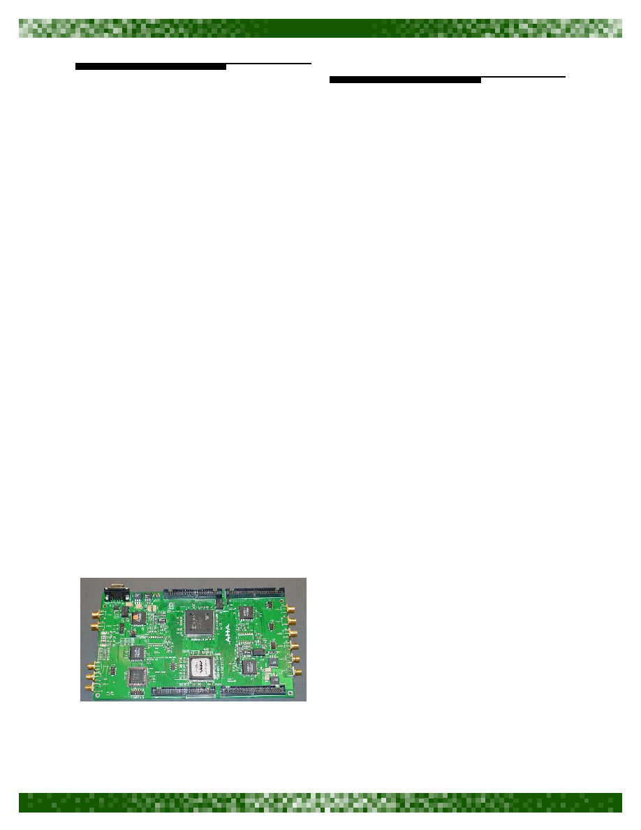
The AHA4540-EVB is a hardware evaluation
board that allows incorporation of the AHA4540
Turbo Product Code (TPC) device in a prototype
communications system or laboratory test
environment. It can be used to demonstrate the
forward error correction (FEC) performance gain
that TPCs offer over other available solutions. The
EVB supports simultaneous encoding and decoding
of a serial or parallel data stream. The board can be
programmed and configured via an RS-232
interface connected to a PC running the included
configuration software to support a wide variety of
code configurations.
The AHA4540-EVB can be interfaced with a
standard Bit Error Rate Tester (BERT) for data
source and data sink or other communications
hardware connected to the uncoded side of the EVB.
On the channel side of the EVB, coded data is
output from the encoder and connected to a modem
or other hardware channel model and then input
back into the EVB after demodulation.
The AHA4540 device is a single-chip Turbo
Product Code (TPC) Forward Error Correction
(FEC) Encoder/Decoder. This device integrates
independent TPC encoder and decoder functions,
and configurable for full or half duplex operation. In
addition to TPC coding, the device includes helical
interleaving, CRC computation and detection,
digital modlation/ demodulation (8PSK, QPSK, 16/
64/256 QAM), LLR mapping and pseudo random
bit stream scrambling. Each of these functional
blocks can be independently bypassed. When
connected with a PC for configuration via the RS-
232 interface the AHA4540-EVB is fully
programmable for a wide range of coding
configurations and allows all registers in the
AHA4540 device to be accessed for configuration.
Figure 1:
AHA4540-EVB Photo
1.1
CONVENTIONS, NOTATIONS AND
DEFINITIONS
� Active low signals have an "N" appended to the
end of the signal name. For example, MCSN and
RESETN.
� Channel Rate - The rate at which encoded data is
output from the device when encoding or input to
the device when decoding. Note that system
channel rate may be different due to external
synchronization marks or other overhead.
� Code block - A data stream to be encoded or
decoded is segmented into blocks for processing
by the AHA4540. Data in a code block is
configured as either a 2D or a 3D array.
� Code rate - Ratio of the number of data bits to the
number of data and ECC bits.
� Data rate - The rate at which unencoded data is
input to the device when encoding or output from
the device when decoding.
� Full iteration - Decoding all axes of an array (all
rows and columns).
� Hard Decision Array (HDA) - The hard decision
output. Data is stored as one bit per location.
� Hex values are represented with a prefix of "0x",
such as register "0x00". Binary values do not
contain a prefix.
� Latency - The time from the first bit of an incoming
block till the first bit of the same block out.
� (n1,k1)x(n2,k2) - A general representation of a
2D block code for use in the descriptions to follow
in this specification. For example, in a
(64,57)x(64,57) code; n1,n2=64 represents the
length of the data + ECC bits, and k1,k2=57
represents the length of only the data bits. 3D
codes are represented as (n1,k1)x(n2,k2)x(n3,k3)
� Soft value - Input to the decoder from either an
Analog/Digital Converter (ADC) or digital
demodulator.

comtech aha corporation
Page 2 of 37
A subsidiary of Comtech Telecommunications Corporation
PS4540evb_0405
1.2
FEATURES
PERFORMANCE:
� 148 MHz maximum clock input (S_UCLK,
S_CCLK)
� 148 Mbits/sec maximum serial data rate
� Simultaneous independent TPC encoding and
decoding
� Access to registers in the AHA4540 device
� Up to 4 bit soft decision input to TPC decoder
� On-board synchronization in the AHA4540
� On-board AHA4540 includes CRC insertion and
detection
INTERFACE:
� SMA connectors for all clock and data signals on/
off board
� 2 frequency synthesizers on board generate
payload side clocks at frequencies up to 60 MHz
� User can supply payload and channel side bit
clocks up to 148 MHz max frequency
� RS-232 control interface for board configuration
and monitoring
GENERAL:
� PCB form factor (5.30" x 8.80")
� On board LED status indicators
� Requires 5V power supply @ 2.0 A
� Requires Windows PC for configuration control
via RS-232 port
� SMA connectors are used for inputs and outputs
for all high speed serial interfaces
1.3
SYSTEM REQUIREMENTS
�
5.0V Power is supplied to the AHA4540-EVB
by the user's power supply. (2.0 Amps
maximum)
�
Programming of the EVB requires a Pentium
class PC running Windows
�
95, 98 or NT with
a RS-232 port.
1.4
MODES
Mode 1:
SERIAL
Uses RS-232 w/ AHAESB windows
software for configuration. This mode
allows the user to easily switch between
codes using an AHAESB script. Data is
transfered to and from the device through
serial SMA connectors. This mode is
selected when internal control register
(0x08) bit 0 and bit 1 are cleared, and the
CDATA MAP register (0x20) is set to
0x00.
Mode 2:
PARALLEL
Uses RS-232 w/ AHAESB windows
software for configuration. This mode
allows the user to easily switch between
codes using an AHAESB script. Data is
transfered to and from the device through
parallel flat cable connectors. This mode is
selected when internal control register
(0x08) bit 1 is asserted and register 0x20,
CDATA MAP register is programmed to
0x01. USER_EDATA is always enabled
and active. It must always be configured as
8 bits wide. USER_DDATA is always
enabled. Bits 2 and 5 of Internal Control
register (0x08) should be set to enable the
USER_DACPT signal.
comtech aha corporation
PS4540evb_0405
A subsidiary of Comtech Telecommunications Corporation
Page 3 of 37
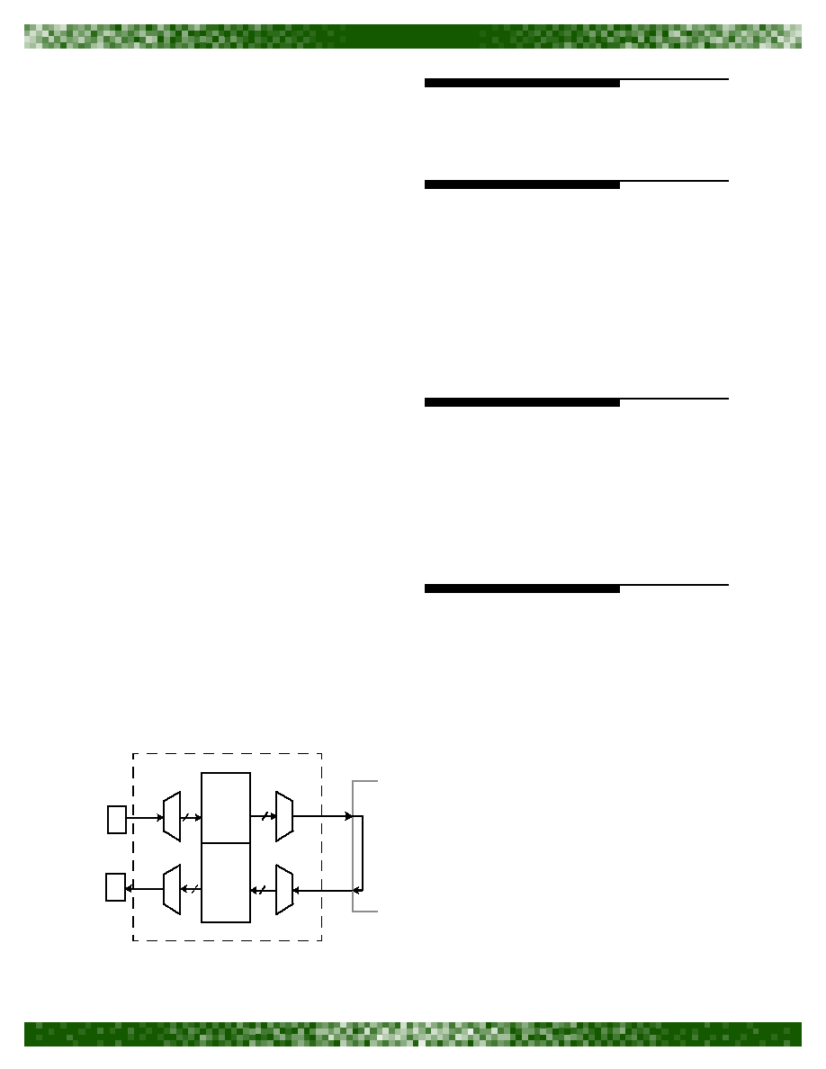
2.0
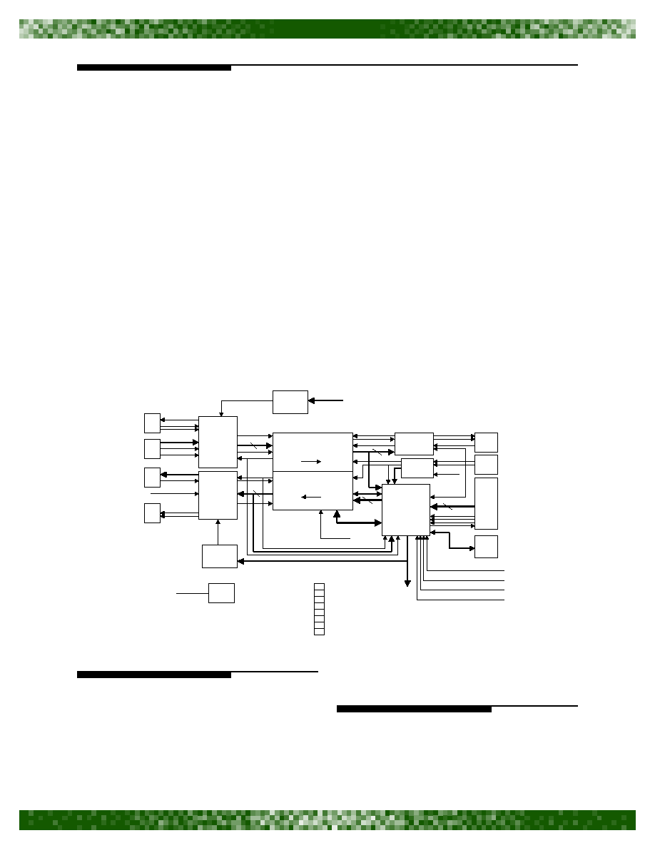
FUNCTIONAL OVERVIEW
The AHA4540 simultaneously encodes and
decodes user provided data using Turbo Product
Codes (TPCs). User provided data is clocked into
the EVB serially using signals S-UCLK and
S_UDATA from coaxial SMA connectors, or with
parallel 8-bit transfers using USER_UDATA from
the parallel connector JP3 and ready/accept
handshake signals. In Figure 2, CPLD_1 contains
the multiplexor that selects either serial data with
clock, or parallel data from the USER_UDATA bus.
Control of this multiplexor is via the AHAESB
Windows software provided. The TPC encoder in
the AHA4540 device encodes the data, adds FEC
bits, then outputs the data to CPLD_3 where the
data gets serialized and transmitted to the channel
along with the clock, S_EDATA and S_ECLK, and
also driven out in 8-bit wide format to the
USER_EDATA bus on JP4.
Once the data is output from the evalutation
board on either the serial or parallel encoded data
interfaces, it is transmitted through an external
channel where the data is corrupted by the addition
of noise resulting in data bit errors. This corrupted
data is clocked into the evaluation board serially
using S_CCLK and S_CDATA or using the
USER_CDATA 16-bit wide parallel input bus on
JP5.
The S_CDATA signal is useful for wrapping
around hard decision channel data back into the
AHA4540 TPC decoder. For soft decision data the
16-bit parallel port must be used. The CDATA port
of the AHA4540 accepts up to 16-bits per clock
transfers of received channel data. This data may be
I,Q data or soft metrics. The chip can accept up to
four I,Q pairs or four soft metrics per transfer. In
serial streaming mode the received serial channel
data is deserialized into four soft metrics with the
lower 3 bits of each metric forced to zero in the
FPGA. The TPC decoder in the AHA4540 corrects
the data errors and outputs the corrected blocks
through CPLD_2 in both serialized clock and data
format, S_DDATA, S_DCLK, and parallel format
to the USER_DDATA bus on JP2.
Figure 2:
AHA4540-EVB Block Diagram
2.1
ENCODING OPERATION
The AHA4540 (U1) performs TPC encoding
one block at a time. For example, a 2D block with a
(n1,k1)x(n2,k2) code, would correspond to an input
block size of k1 x k2 bits. Once an entire block of
data has been input to the AHA4540, it is encoded.
The encoder would compute the extra ECC bits and
output n1 x n2 bits. On board Serializers and
Deserializers allow the user to accept a continuous
data stream.
2.1.1
ENCODE DATA INPUT
The AHA4540-EVB takes serial data on the
S_UDATA SMA connector. The input data is
clocked into the EVB using the S_UCLK signal.
Input data is latched on the rising edge of the
AHA4540
Encoder
Decoder
CPLD1
Deserializer and
2:1 MUX
Frequency
Synthesizer
1
CPLD4
Deserializer
FPGA
16
8
8
CPLD2
Serializer
and Buffer
16
Oscillator
86 MHz
SERIAL
I/O
(SMA)
UPI
UD
DD
ED
CD
BERT
TRX
(SMA)
BERT
REC
(SMA)
LCHCLK
PC I/O
RS232
NOTES:
1. SMA connectors to BERT and channel Serial I/O
2. USER I/O Conn is through two 50-pin flat cables
8
PAR
I/O
DPCLK
Unused
SW1
SW2
SW3
LEDs
CPLD3
Serializer
UCLK
ECLK
EPCLK
(43M)
DCLK
CLK_SYNC
CCLK
CLK_86M
FPGA_DACPT
USER_UDATA
UACPT
URDY
USER_URDY
HCHCLK
USER_DACPT
USER_DDATA
PAR
I/O
PAR
I/O
PAR
I/O
USER_UCLK
SERIAL
I/O
(SMA)
CLK_86M
CLK_86M
Encoder Channel Clock
Encoder Payload Clock
70Mhz
70Mhz
Frequency
Synthesizer
2
Decoder Channel Clock
Encoder Payload Clock
Decoder Payload Clock
Frequency
Control
Frequency
Control
Unused
GOUT_1
GOUT_0
FPGA RDY
D1
D2
D3
D4
D5
D6
D7
D8
comtech aha corporation
Page 4 of 37
A subsidiary of Comtech Telecommunications Corporation
PS4540evb_0405
S_UCLK signal. An output signal CLK_SYNC
may be used as a clock request signal for S_UCLK.
Parallel input data mode is supported via the
USER_UDATA bus on JP3. The data gets passed
through CPLD_1 to the AHA4540. To select
parallel mode operation the Internal Control register
0x08 bit-6 must be set by writing the register in a
user software script. The scripts are either
interactively loaded or named USERTESTx.AHA
which allows them to connect to one of the buttons
on the AHAESB control software window.
2.1.2
ENCODE DATA OUTPUT
Encoded data is output from the AHA4540-
EVB encoder serially on the S_EDATA signal.
Output data is strobed out of the EVB on the falling
edge of the S_ECLK signal. This signal is the
inverted user supplied clock (CSCLK, J9. Encoded
data can be strobed out from the EVB at data rates
up to 148 Mbits/sec.
Parallel encoded data is available on the
USER_EDATA bus on connector JP4. The Internal
Control register 0x08 bits 0,1 must be set to 0x02 to
enable the USER_EACPT signal. USER_ERDY
and USER_ECLK are always driven on JP4.
2.2
DECODING OPERATION
The AHA4540 device on the EVB also operates
as a TPC decoder, operating on a single block at a
time. For a 2D block with a (n1,k1)x(n2,k2) code, n1
x n2 symbols are input for each block. Once an entire
block of data is received by the AHA4540 decoder,
it is iteratively decoded, corrupted bits are corrected
and then the block of k1 x k2 data bits is output from
the decoder.
2.2.1
DECODE DATA INPUT
The input data to the AHA4540 decoder device
on the EVB can be either hard decision data (1 bit)
or soft decision data (up to 4 bit soft decision via
USER_CDATA on the parallel connector JP5).
Hard decision serialized data can use the S_CDATA
SMA connector for data input. The rising edge of
S_CCLK is used to clock in the data when the
serialized channel input is used.
Parallel received data from the channel may be
used by enabling the USER_CDATA port on JP5.
This is a 16-bit bus that gets passed straight through
to the AHA4540 TPC decoder. Enabling this
requires writing the Internal Control register 0x08
bits 0,1 to 0x02. USER_CCLK is passed through to
the AHA4540 CCLK signal in this mode of
operation.
2.2.2
DECODE DATA OUTPUT
The AHA4540 decoder outputs the decoded data
stream serially from the EVB on the S_DDATA SMA
connector J4. Decode data is clocked out using the
rising edge of S_DCLK output signal on SMA
connector J6. Decoded data is output from the EVB at
the programmed data rate at rates up to 148 Mbit/sec.
Maximum data rate if using an on-board synthesizer
to generate the payload bit clock is 60 Mbit/sec.
Parallel decoded data output is available on
connector JP3. The data bus and USER-DRDY are
always driven. Enabling USER_DACPT requires
setting USER_SEL and PSEL2 (bits, 2,5) in the
Internal Control register (0x08).
2.3
CLOCK SOURCES
2.3.1
CRYSTAL OSCILLATORS
There are a total of three crystal oscillators on
the EVB. Crystal (Y1) at 86.0 MHz is used for the
AHA4540 processing clocks DPCLK and EPCLK
(86 Mhz / 2). Crystal (Y2) at 3.6864 MHz is a
reference for the RS232 interface in the FPGA.
Crystal (Y3) at 30.0 MHz is the reference clock for
the frequency synthesizers (U20,U21). The
frequency synthesizers multiply this clock by six
and use an internal reference clock of 180 Mhz.
2.3.2
FREQUENCY SYNTHESIZERS
The frequency synthesizers defines the uncoded
data rates through SMA connector (J2)
CLK_SYNC and (J6) S_DCLK. Interactive
feedback control inside the FPGA automatically
adjusts the uncoded data rate frequency to prevent
data underflows or overflows, thus frequency
locking the payload side data rate to the channel side
data rate.
Maximum frequency for the two synthesizers is
60 MHz. They are programmable by writing the 4-
Byte control value in a user script, or selecting the
Clock Synth Tab in the Configure window, typing in
the frequencies in MHz and selecting the set button.
To determine the 4-Byte value use the equations
below. The first equation determines the code rate
including frame sync bits, and the next one
calculates the 4-Byte value that gets programmed
via the user script.
comtech aha corporation
PS4540evb_0405
A subsidiary of Comtech Telecommunications Corporation
Page 5 of 37
SYNTH_CLK_FREQ = Payload Data Rage = [Message_data_bits / (Message_data_bits + ECC_bits +
Synchronization_bits)]*CHANNEL_CLCK_FREQ
[1]
4-Byte value = [Synth Byte 1, Synth Byte 2, Synth Byte 3, Synth Byte 4] = B1,B2,B3,B4
[2]
B1,B2,B3,B4 = [SYNTH_CLK_FREQ * 2
32
] / 180
Programming Synthesizer 1, Encoder Payload Clock, requires writing this value to registers 0x0C,
0x0D, 0x0E, and 0x0F.
2.4
SYNCHRONIZATION SUPPORT
All synchronization support is performed by the AHA4540. See AHA4540 product specification for
more infomation.
2.4.1
LED STATUS DEFINITIONS (D1-D8)
Table 1:
LED Definition
2.4.2
SWITCH DEFINITIONS
Table 2:
Switch Definition
2.4.3
JUMPER CLOCK CONFIGURATION (JP7)
Table 3:
Jumper Clock Configuration
2.4.4
JUMPER CLOCK CONFIGURATION (JP8)
Table 4:
Jumper Clock Configuration
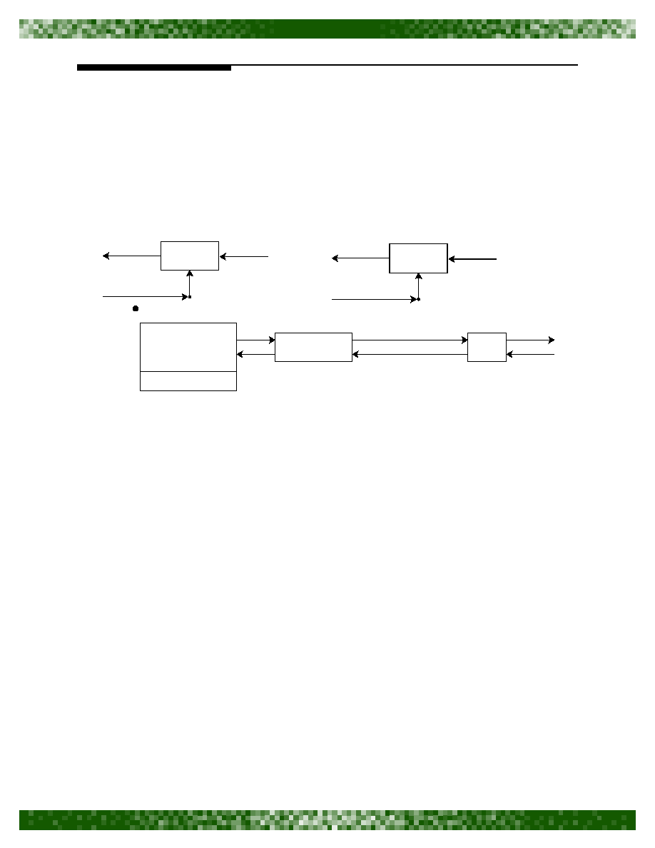
2.5
LOOPBACK - TEST 1
Test 1 routes the uncoded input data to the
output data through the entire data path of the EVB
including the output connections for the user
channel. The encoder and decoder are configured
for a (128,120)
2
code and the channel rate is 50
MHz. Connect the cables to the BERT as specified.
Connect an additional SMA to SMA jumper
between S_EDATA to S_CDATA and S_ECLK to
S_CCLK.
LEDS LED
DEFINITION
D1
GOUT_0
D2
GOUT_1
D3
Unused
D4
Unused
D5
SW1
D6
SW2
D7
SW3
D8
FPGA Programmed
PUSH
BUTTON
SWITCH DEFITION
SW0
Reprogram FPGA
SW1
Undefined
SW2
Undefined
SW3
Reset AHA4540, AD9851 and FPGA
JP7 PINS
1,2,3
ENCODER CLKSYNC SOURCE
1-2
VCO1
2-3
Frequency Synthesizer 1
JP8 PINS
1,2,3
DECODER CLKSYNC SOURCE
1-2
VCO2
3-4
User Supplied S_DCLK_IN SMA
(J13)
5-6
Frequency Synthesizer 2
comtech aha corporation
Page 6 of 37
A subsidiary of Comtech Telecommunications Corporation
PS4540evb_0405
Connect appropriate cables as specified below
for proper operation.
BERT transmitter connections:
� S_UDATA (SMA J1): Data input from BERT
transmitter
� S_UCLK (SMA J3): Clock input from BERT
transmitter
� CLK_SYNC (SMA J2): Optional clock request to
BERT transmitter
BERT receiver connections:
� S_DDATA (SMA J4): Data output to BERT
receiver
� S_DCLK (SMA J6): Clock output to BERT
receiver
Note:
Cable lengths for S_UDATA and S_UCLK
should be approximately the same length
shielded coax (recommended RG58c/u or
equivalent, Zo=50ohms). Cables for S_DDATA
and S_DCLK should be approximately the same
length. (Max length 4ft.)
Channel Clock source:
CSCLK (SMA J9): Connect to external clock
source with frequency = 50.06 MHz.
�
Frequency other than this will require changing
the 4-Byte value for the encoder payload clock
synthesizer in the software script named
TEST1.AHA.
Channel Loopback cables
� Connect S_ECLK (SMA J10) to S_CCLK (SMA
J7)
� Connect S_EDATA (SMA J8) to S_CDATA
(SMA J5)
� Connect CLK_SYNC (J2) to S_DCLK_IN (J13).
This allows the the Encoder synthesizer to be used
for both payload rate clock sources.
Figure 3:
Encode/Decode Loopback - Test 1
Datapath
JP7 Jumper Settings: (2-3)
JP8 Jumper Settings: (2-3)
2.6
LOOPBACK - TEST 2
Same system configuration as TEST 1. This
loopback test uses the (16,11)
3
TPC code.
2.7
LOOPBACK - TEST 3
This test implements the (128, 120)
2
code, at
50.06 Mb/s channel rate, and allows two separate
channel clocks and payload clocks. Both on board
synthesizers are used and locked to their appropriate
channel rate bit clock.
Same system configuration as TEST 1 except
the following:
1) Disconnect cable to S_DCLK_IN(J13)
2) Move jumper JP8 to pins 5,6
2.8
LOOPBACK TEST 4
This is a pass through test requiring one clock
source for all channel clocks and payload side
clocks and runs at any frequency up to 148 MHz.
Same system configuration as TEST 1 except
the following:
1) CLK_SYNC (SMA J2) is not used. Connect
the clock request on the BERT Transmitter
to the channel bit clock source.
2.9
LOOPBACK - TEST 5
This test uses the same system configuration as
TEST 1. It is a high speed, 148.3 Mb/s channel rate
test with the (16,11)
3
TPC code and a payload data
rate of 48 Mb/s. Decoder iterations are set to 3.
BERT
TX
Encoder
BERT
RX
Decoder
8
8
8
8
AHA4540 - EVB
Payload
Channel
Loopback
Cables

comtech aha corporation
PS4540evb_0405
A subsidiary of Comtech Telecommunications Corporation
Page 7 of 37
2.10
EVB CONFIGURATION FOR MODE 1
1) Connect 5V power supply to JP9 pins 1 and 2.
2) Connect RS-232 cable to EVB and Host PC.
3) Start AHAESB software on Host PC.
4) Connect to board by pressing Connect button
(set serial port parameters correctly).
5) Connect SMA-BNC cables to EVB, Data
Source/Sink, and Channel Source/Sink as
described in Section 2.5.
6) Run AHAESB script to setup the board and
program the AHA4540 device to desired
configuration.
7) EVB should start encoding, decoding, and
passing data.
2.11
MODE 1 SCRIPT WRITING
1) Board reset.
2) Program payload frequency.
3) Program block sizes.
4) Program Sync Word Length.
5) Program the encoder/decoder configuration
into the AHA4540 device:
5.1) Assign the AHA4540 address byte into
register 0x04.
5.2) Assign the AHA4540 data byte into
register 0x05.
5.3) Send a write strobe to the AHA4540
device by using the following line, "inc
pluto_write_strobe.aha".
5.4) (optional) You may read back your
written value with the following line, "inc
pluto_read_strobe.aha", this will verify
that the correct value was written to the
AHA4540 device.
5.5) Repeat these three or four steps for all
registers in the TPC encoder/decoder that
need to be written after a reset.
6) (Optional) The script may be tied directly to a
user test button and executed by selecting the
button on the AHAESB software window. This
requries naming the script usertest1.AHA,
usertest2.AHA, ... usertest5.AHA and locating
it in the same directory as the AHAESB.EXE
executable software.
2.12
SOFTWARE INSTALLATION
The AHAESB software (AHAESB.exe) is used
to configure and monitor the EVB. This software is
shipped with the EVB.
2.13
QUICK START
This section briefly describes the steps necessary
to power-up the EVB and get Loopback Test1
running, using a standard Bit Error Rate Transmitter/
Receiver (BERT).
1) Install the AHAESB per instructions for Mode
1 above.
2) Provide correct voltage to the EVB 5.0V/GND
Power Connector.
3) Connect SMA cables as shown below:
BERT transmitter connections:
� S_UDATA to BERT data output
� S_UCLK to BERT clock output
� CLK_SYNC to BERT external clock input
BERT receiver connections:
� S_DDATA to BERT data input
� S_DCLK to BERT clock input
Encode out to Decode in bypass cable:
� S_EDATA to S_CDATA on EVB
� S_ECLK to S_CCLK on EVB
4) Confirm jumpers are connected (2-3), (2-3) for
JP7 and JP8.
5) Connect external clock source to CSCLK (J9)
for the channel bit-rate clock.
6) Connect loopback cable
S_EDATA
S_CDATA.
S_ECLK
S_CCLK.
7) Run Loopback Test 1 by clicking on the
appropriate button in the AHAESB SW.
8) Set up BERT transmitter for TTL signal levels.
Verify these levels with an oscilloscope.
9) Set up BERT transmitter for external clock
sync.
10) BERT receiver should show zero bit errors, and
frequency is 43 MHz.
11) The signal monitors in the right side of the
software window should show alternating zeros
and ones indicating data is flowing from data
source to data sink through the EVB.

comtech aha corporation
Page 8 of 37
A subsidiary of Comtech Telecommunications Corporation
PS4540evb_0405
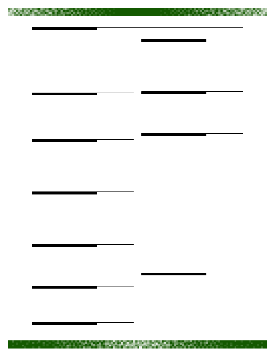
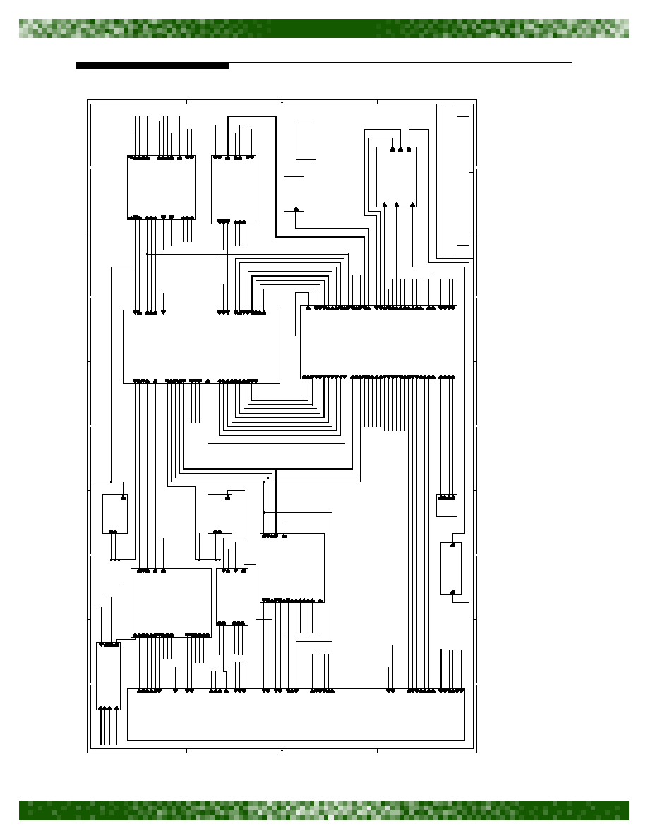
3.0
HARDWARE DESCRIPTION
Figure 4:
AHA4540-EVB Major Component Diagram
Discrete Components
U1:
AHA4540 TPC Encoder/Decoder
U9:
Xilinx Virtex E FPGA, XCV200E-PQ240
U10: SPROM to program FPGA Controller
U11: Altera 7032 CPLD
U13: Altera 7032 CPLD
U14: Altera 7032 CPLD
U15: Altera 7032 CPLD
U5:
Line Driver (Tristatable)
U6:
Line Driver (Tristatable)
U12: Line Driver (Tristatable)
U18: Line Driver (Tristatable)
U19: Line Driver (Tristatable)
U20: Frequency Synthesizer for Payload Data Side
Clock
U21: Frequency Synthesizer for Payload Data Side
Clock
J1:
Unencoded Data (Input)
J2:
Clock Sync for BERT (Output)
J3:
Unencoded Clock (Input)
J4:
Decoded Data (Output)
J5:
Channel Data (Input)
J6:
Decoded Clock (Output)
J7:
Channel Clock (Input)
J8:
Encoded Data (Output)
J9:
Encoder Side Channel Clock (Input)
J10: Encoded Clock (Output)
J13: Decoder Side Channel Clock (Input)
JP6: JTAG Port for Altera CPLD's
JP7: Encoder Side Payload Clock Jumper
JP8: Decoder Side Payload Clock Jumper
JP9: Power Connector
J11: Serial Program Port for FPGA
J12: JTAG Program Port for FPGA
JP2: Decoder Parallel Input:
JP3: Unencoded Parallel Input
JP4: Encoded Parallel Input
JP5: Channel Parallel Input
SW0 - SW1:
Resets
SW2 - SW3: Push Buttons
REG1: 5.0V to 2.5V Regulator
REG2: 5.0V to 12V Regulator
REG3: 5.0V to 1.8V Regulator
REG4: 5.0V to 3.3V Regulator
JDR1: RS-232 Connector
Y1:
86.0 Mhz Clock for AHA4540 EPCLK and
DPCLK (EPCLK = DPCLK/2)
Y3:
30 MHz Crystal for Frequency Synthesizer
Reference Clock
Y2:
3.6864 MHz Crystal for Serial Port
Communication base frequency
JP5
JP4
V9
V1
U14
V11
Y3
REG1
REG2
JP3
JP2
V10
J11/J12
V13
V15
REG4
JDR1
Y1
Y2
J9
J8
J2
J1
J3
J10
J7
J5
J4
J6
J13
D1-
D8
V20
JP9
SW0
-
SW3
V6
JP6
J18
REG3
V19
V21
V6
v1
2
v18
comtech aha corporation
PS4540evb_0405
A subsidiary of Comtech Telecommunications Corporation
Page 9 of 37
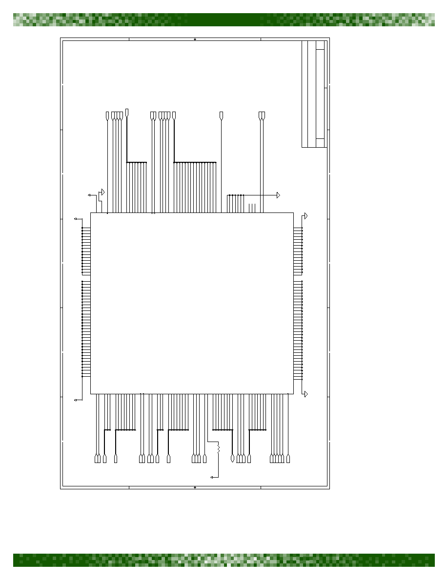
4.0
FPGA CONTROLLER TOPLEVEL DESCRIPTION
Hierarchical FPGA VHDL Flow
Ra_pipe - Ready / Accept handshaking pipe stage
UART - Communication with the PC via RS-232
port. The UART block can read and
write registers.
RS232con - Takes in Serial RS-232 data and
converts it to byte wide data
CZX - Clock Zone crossing boundary
UCON - Microcontroller interface. Manages
reads and writes to the register stack.
Programs the Frequency Synthesizer.
Freq_ctrl_r5 - This block determines if the
payload date frequency should be
increased or decreased to avoid an
underflow or overflow.
Micro_reg - 8-bit microcontroller register
Figure 5:
FPGA Block Diagram
UART
RS-232
MICROCONTROLLER
(UCON)
EVB REGISTERS
T
x
R
x
FREQUENCY
CONTROL
CLK_SYNC
S_UCLK
CSCLK
FREQUENCY
CONTROL
S_DCLK
S_DCLK_IN
S_CCLK
comtech aha corporation
Page 10 of 37
A subsidiary of Comtech Telecommunications Corporation
PS4540evb_0405
5.0
AHA4540-EVB COMMUNICATION SOFTWARE
Communication and control of the AHA4540-
EVB is via the RS-232 interface to a host PC. The
AHAESB.exe software is provided for this purpose.
The AHAESB software operates under Windows
�
95, 98, 2000, or NT. The AHAESB software allows
the user to configure the AHA4540 device on the
EVB as well as the clock synthesizers and FPGA
registers.
5.1
OPERATION OF AHAESB
SOFTWARE
To operate the AHAESB software, click on the
AHA4540-EVB icon on the Windows
�
desktop or
alternatively execute the program AHA4540
EVB.exe from either a DOS window or the
Windows
�
RUN menu. An application window for
AHA4540-EVB should open.
5.1.1
CONNECT BUTTON
This button enables connection from the PC to the
AHA4540-EVB via the RS-232 cable. A pop-up menu
will appear allowing the user to configure the
communication link between host PC and the
AHA4540-EVB. Configuration parameters are: Comm
Port (COM1,2,3 or 4), Number of Stop Bits (defaults to
1), and Data Rate (defaults to 115,200 Baud).
5.1.2
CONFIGURE BUTTON
This menu allows configuration of the clock
synthesizers. Registers in the AHA4540 device can
be accessed. See the AHA4540 Product
Specification for a complete list of AHA4540
registers. The clock synthesizers are also
programmable in the configure menu. Data rate can
be controlled from this menu.
5.1.3
INTERACTIVE MODE WINDOW
The interactive mode window allows the user to
control signals with the FPGA to allow customized
control of the EVB. Script files containing
instructions for the EVB can be loaded and saved
from this window.
5.1.4
LOG WINDOW
The Log Window records all communication
transactions between the PC and the EVB.
If an error were encountered while communicating
with the EVB it would be recorded here.
5.1.5
RESET STATUS
Indicates whether or not the board is in reset.
5.1.6
USER TEST MODES
These buttons can be linked to user scripts
created by the customer. These buttons provide an
easy and quick way to access/run user defined
scripts. They must be named usertestX.aha, where X
is the button number and reside in the same directory
as the executable file for the software. The self test
bit must be off and the number of soft bits set.
5.1.7
TEST MODES
These buttons are linked to test scripts created
by AHA. These buttons provide an easy and quick
way to access/run AHA defined board functionality
tests. They must be named testX.aha, where X is the
appropriate button number.
5.1.8
AHAESB SCRIPT SYNTAX
The syntax is similar to standard assembly with
only a few operations.
WRA � Command used to write to a register in the
FPGA.
i.e. WRA 1E 0F
This would write a 0F (15-bit sync word
length) to register 1E
RDA � Command used to read a register in the
FPGA
i.e. RDA 1E
If the above write was executed first, the
response from the interactive window
would yield "0F".
inc �
Command used to include another
AHAESB script in the current script. Useful
for hierarchical script programming.
i.e. inc reset.aha
SLP � Command used to make the AHAESB SW
wait a period of time before the next
command is issued.
i.e. SLP 3E8
Sleep for 1ms
RST � Generates a board reset
5.2
ESB STATUS
The EVB status window displays the
frequencies of the two on-board frequency
synthesizers, Encoder Synthesizer and Decoder
Synthesizer. It also includes data monitors that
monitor some of the signals on the board indicating
whether the signals are changing or not.
comtech aha corporation
PS4540evb_0405
A subsidiary of Comtech Telecommunications Corporation
Page 11 of 37
6.0
REFERENCE GUIDE TO PROGRAMMING EVB REGISTERS
This guide describes all user accessible registers on the evaluation board.
Table 5:
List of EVB Registers with Address
ADDRESS (HEX)
NAME
00
LOCAL_UART_ADDRESS
01
RESETS
02
CHIIP_SELECTS
03
CONTROL_SIGNALS
04
ADDRESS
05
OUTPUT_DATA
06
INPUT_DATA
07
INTERRUPT_STATUS
08
INTERNAL_CONTROL
09
OUTPUT_PULSE
0B
BITFILE_VERSION_REGISTER
0C
ENCODE_FREQUENCY_SYNTH_BYTE_1
0D
ENCODE_FREQUENCY_SYNTH_BYTE_2
0E
ENCODE_FREQUENCY_SYNTH_BYTE_3
0F
ENCODE_FREQUENCY_SYNTH_BYTE_4
10
DECODE_FREQUENCY_SYNTH_BYTE_1
11
DECODE_FREQUENCY_SYNTH_BYTE_2
12
DECODE_FREQUENCY_SYNTH_BYTE_3
13
DECODE_FREQUENCY_SYNTH_BYTE_4
20
CDATA_MAP
28
SYNTHESIZERS_CONTROL
29
ENCODE_SYNTH_DELTA_BYTE_2
2A
ENCODE_SYNTH_DELTA_BYTE_3
2B
ENCODE_SYNTH_DELTA_BYTE_4
2C
DECODE_SYNTH_DELTA_BYTE_2
2D
DECODE_SYNTH_DELTA_BYTE_3
2E
DECODE_SYNTH_DELTA_BYTE_4
30
ENC_PAYLOAD_BITS_LSB
31
ENC_PAYLOAD_BITS_MSB
32
ENC_CHANNEL_BITS_LSB
33
ENC_CHANNEL_BITS_MSB
34
ENCODE_SYNC_LENGTH
35
DEC_PAYLOAD_BITS_LSB
36
DEC_PAYLOAD_BITS_MSB
37
DEC_CHANNEL_BITS_LSB
38
DEC_CHANNEL_BITS_MSB
39
DECODE_SYNC_LENGTH
43
SIGNAL_ACTIVITY

comtech aha corporation
Page 12 of 37
A subsidiary of Comtech Telecommunications Corporation
PS4540evb_0405
6.1
REGISTER DESCRIPTION
0x00
LOCAL UART ADDRESS
reset value [0x00]
Local storage of register address for UART "RDA" and "WRA" commands
0x01
RESETS
reset value [0x00]
Reset signals to devices on board.
0x02
CHIP SELECTS
reset value [0x00]
bit 0 : AHA4540 chip select, MCSN
0x03
CONTROL SIGNALS
reset value [0x00]
Control signals to on board devices.
bit 7 :
Unused, always asserted low
bit 6 :
Unused, always asserted low
bit 5 :
Unused, always asserted low
bit 4 :
Unused, always asserted low
bit 3 :
Unused, always asserted low
bit 2 :
Unused, always asserted low
bit 1 :
AHA4540 read strobe, MRDN_DSN
bit 0 :
AHA4540 write strobe, MWRN_RWN1
0.04
ADDRESS
reset value [0x00]
Address bus to AHA4540 device, MA[5:0}
0x05
OUTPUT DATA
reset value [0x00]
Data bus to AHA4540 device, MDATA[7:0]
0x06
INPUT DATA
reset value [0x00]
Data bus from AHA4540 device, MDATA[7:0]
0x07
INTERRUPT STATUS
reset value [undefined]
Interupts from AHA4540 and GOUTx signals
bit 7 :
Unused, always asserted low
bit 6 :
Unused, always asserted low
bit 5 :
Unused, always asserted low
bit 4 :
Unused, always asserted low
bit 3 :
Unused, always asserted low
bit 2 :
AHA4540 GOUT[1] signal
bit 1 :
AHA4540 GOUT[0] signal
bit 0 :
AHA4540 Interrupt, MINTN
0x08
INTERNAL CONTROL
reset value [0x00]
Controls mode of board.
bit 7 :
unused, always asserted low
bit 6 :
Psel_1, enables USER_UDATA and USER_UCLK
bit 5 :
Psel_2, when set along with User_sel enables USER_DACPT
bit 4 :
Psel_4, not used
bit 3 :
Chsel, not used
bit 2 :
User_sel, when set along with Psel_2 enables USER_DACPT
bit 1 :
Loopback select_1
bit 0 :
Loopback select_0

comtech aha corporation
PS4540evb_0405
A subsidiary of Comtech Telecommunications Corporation
Page 13 of 37
Loopback select bits 1,0
0x00 :
Serial Streaming
0x01 :
Edata to Cdata internal loopback
0x02 :
USER_EDATA, USER_CDATA parallel ports, and USER_CCLK enabled
0x03 :
CRDY and EACPT always asserted high
0x09
OUTPUT PULSE
reset value [0x00]
Output Control Pulses.
0x0B
BIT FILE VERSION
reset value [0x0B]
Returns the bit file version. The upper 4 bits represent the whole number part and the lower 4 bits represent
the fractional part.
0X0C
ENCODE FREQUENCY SYNTH BYTE 1
reset value [0x00]
0x0D
ENCODE FREQUENCY SYNTH BYTE 2
reset value [0x00]
0x0E
ENCODE FREQUENCY SYNTH BYTE 3
reset value [0x00]
0x0F
ENCODE FREQUENCY SYNTH BYTE 4
reset value [0x00]
These registers set the output frequency of U20, the eoncoder path synthesizer according to the following
equation:
0x10
DECODE FREQUENCY SYNTH BYTE 1
reset value [0X00]
0X11
DECODE FREQUENCY SYNTH BYTE 2
reset value [0x00]
0X12
DECODE FREQUENCY SYNTH BYTE 3
reset value [0x00]
0X13
DECODE FREQUENCY SYNTH BYTE 4
reset value [0x00]
These register set the output frequency of U21 the encoder path synthesizer according to the following
equation:
0x20
CDATA MAP
reset value [0x00]
Maps CDATA port into the AHA4540 as follows
Register Value
Mapping
0x00
Deserialized Hard decision data from SMA (S_CDATA) 4 soft metrics per
transfer
0x01
16-bit USER_CDATA mapped straight through
0x02
EDAT to CDATA internal loopback
0x03
USER-EDATA to USER_CDATA external loopback (requires external
wire jumpers).
Others
16-bit USER_CDATA mapped straight through
0x28
SYNTHESIZERS CONTROL
bits 7-2: Unused
bit 1 :
When set the decoder synthesizer uses the fixed register programmed value for the frequency
delta set in registers 0x2C, 0x2D, and 0x2E as follows:
NEW_SYNTH_VALUE = [SYNTH_BYTE 1, 2, 3, 4] +/- [0,00, DELTA_BYTE 2, 3, 4]
Byte 4 is the least significant Byte of the 4-Byte value
bit 0 :
When set the encoder synthesizer uses the fixed register programmed value for the frequency
delta set in registers 0x29, 0x2A, and 0x2B as follows:
NEW_SYNTH_VALUE = [SYNTH_BTE 1, 2, 3, 4] +/- [0,00, DELTA_BYTE 2, 3, 4]
Byte 4 is the least significant Byte of the 4-Byte value
FREQ
BYTE_1, BYTE_2, BYTE_3, BYTE_4
[
] 100
�
2
32
------------------------------------------------------------------------------------------------------------------- MHz
=
FREQ
BYTE_1, BYTE_2, BYTE_3, BYTE_4
[
] 180
�
2
32
------------------------------------------------------------------------------------------------------------------- MHz
=

comtech aha corporation
Page 14 of 37
A subsidiary of Comtech Telecommunications Corporation
PS4540evb_0405
0x29
ENCODE SYNTH DELTA BYTE 2
reset value [0x00]
0x2A
ENCODE SYNTH DELTA BYTE 3
reset value [0x00]
0X2B
ENCODE SYNTH DELTA BYTE 4
reset value [0x00]
These register values are added or subtracted to the Encoder frequency synthesizer base value in registers
0x0C, 0x0D, 0x0E, 0x0F when enabled in register 0x28
NEW_SYNTH_VALUE = [SYNTH_BYTE 1, 2, 3, 4] +/- [0x00, DELTA_BYTE 2, 3, 4]
Byte 4 is the least significant Byte of the 4-Byte value.
0x2C
DECODE SYNTH DELTA BYTE 2
reset value [0x00]
0x2D
DECODE SYNTH DELTA BYTE 3
reset value [0x00]
0x2E
DECODE SYNTH DELTA BYTE 4
reset value [0x00]
These register values are added or subtracted to the decoder frequency synthesizer base value in registers
0x10, 0x11, 0x12, 0x13 when enabled in register 0x28.
NEW_SYNTH_VALUE = [SYNTH_BYTE 1, 2, 3, 4] +/- [0x00, DELTA_BYTE 2, 3, 4]
Byte 4 is the least significant Byte of teh 4-Byte value.
0x30
ENCODE PAYLOAD BITS LSB
reset value [0x00]
0x31
ENCODE PAYLOAD BITS MSB
reset value [0x00]
Set equal to the block size of the encoder TPC unencoded block.
0x32
ENCODE CHANNEL BITS LSB
reset value [0x00]
0x33
ENCODE CHANNEL BITS MSB
reset value [0x00]
Set equal to the encoder encoded block including the FEC Bits, but not including frame sync bits.
0x34
ENCODE SYNC BITS PER FEC BLK
reset value [0x00]
Set equal to (EFSyncLength x EFSyncFreq) as programmed into the AHA4540
0x35
DECODE PAYLOAD BITS LSB
reset value [0x00]
0x36
DECODE PAYLOAD BITS MSB
reset value [0x00]
Set equal to the block size of the decoder TPC unencoded block
0x37
DECODE CHANNEL BITS LSB
reset value [0x00]
0x38
DECODE CHANNEL BITS MSB
reset value [0x00]
Set equal to the TPC decoder encoded block size including the FEC bits, but not including frame sync bits.
0x39
DECODE SYNC BITS PER FEC BLK
reset value [0x00]
Set equal to (DFSyncLength x DFSync Freq) as programmed into the AHA4540
0x43
SIGNAL ACTIVITY
Indicates activity of selected signal ports by showing current value (multiple reads need to see changes)
bit 7 :
decoder payload clk
bit 6 :
encoder payload clk
bit 5 :
E_CLK
bit 4 :
E_DATA (0)
bit 3 :
C_CLK
bit 2 :
C_DATA
bit 1 :
D_CLK
bit 0 :
D_DATA (0)

comtech aha corporation
PS4540evb_0405
A subsidiary of Comtech Telecommunications Corporation
Page 15 of 37
7.0
REGISTER PROGRAMMING
7.1
AHA4540 REGISTERS
The AHA4540 device on the board is accessible
for programming and status information through the
AH4540-EVB software. From the program select
the interactive button. Here you can read and write
to registers in the FPGA or AHA4540. Refer to the
AHA4540 product specification for a complete
description of all registers in the AHA4540 device.
7.2
FREQUENCY SYNTHESIZERS
Two on board synthesizers are programmed via
the AHAESB software. From the program select the
Clock Synth tab in the configure window. The value
entered for Encoder Synth controls the clock
synthesizer U21. Clock synthesizer U20 is
controled by the entry Decoder Synth. Synthesizer
U21 can also be programmed via user scripts by
writing the desired values to registers 0x0C, 0x0D,
0x0E, 0x0F as outlined in Section 5.1.8 AHAESB
Script Syntax. Synthesizer U20 can be written to
using register 0x10, 0x11, 0x12, 0x13.
The ratio of the values entered for clock
synthesizers should exactly match the code rate of
the code (including synchronization bits) as shown
in the following equation:
7.3
AHA4540-EVB FPGA REGISTERS
See Section 6.0 REFERENCE GUIDE TO
PROGRAMMING EVB REGISTERS and Section
6.1 Register Description.
Data Rate
Channel Rate
--------------------------------
Data Bits
Data Bits
ECC Bits
Sync_word_bits
+
+
-------------------------------------------------------------------------------------------------
=
comtech aha corporation
Page 16 of 37
A subsidiary of Comtech Telecommunications Corporation
PS4540evb_0405
8.0
SIGNALS IN/OUT OF EVB
8.1
EVB MAIN BOARD
9.0
ELECTRICAL SPECIFICATIONS
9.1
BOARD POWER
Power is provided from the users power supply.
5 Volts DC at 2.0 Amps JP9 pins 1 and 2.
Power consumption varies depending on customer configuration, but a minimum of 2A is required for
factory configuration.
9.2
SIGNAL REQUIREMENTS
BERT signals at SMA connectors should be TTL levels. Program BERT for threshold levels of
approximately 1.5V. Validate TTL levels using an oscilloscope.
PIN
CONNECTOR
FUNCTION
TYPE
J1
SMA
S_UDATA
Input
J3
SMA
S_UCLK
Input
J2
SMA
CLK_SYNC
Output
J8
SMA
S_EDATA
Output
J10
SMA
S_ECLK
Output
J9
SMA
CSCLK
Input
J4
SMA
S_DDATA
Output
J6
SMA
S_DCLK
Input
J13
SMA
S_DCLK_IN
Input
J7
SMA
S_CCLK
Input
J5
SMA
S_CDATA
Input
JDR1
9 pin DSUB
RS232 Serial Data Connector
I/O
J11
.1" Header
FPGA Serial Program Header
Input
J12
.1" Header
FPGA JTAG Connector
I/O
JP6
.1" Header
CPLD JTAG Connector
I/O
JP7
1x3
Encoder Payload Clock Selector Control
JP8
2x3
Deocder Payload Clock Selector Control
JP9
2x3
DC Power Connector
I/O, Pwr
comtech aha corporation
PS4540evb_0405
A subsidiary of Comtech Telecommunications Corporation
Page 17 of 37
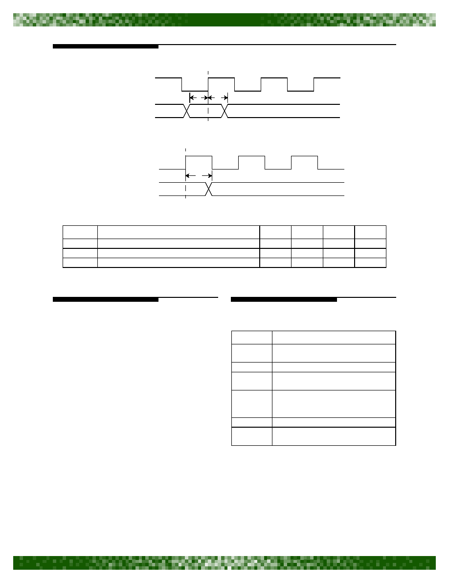
10.0 TIMING SPECIFICATIONS
Figure 6:
Data Input Timings
Figure 7:
Data Output Timings
Table 6:
Data Input/Output Timings
11.0 BOARD DIMENSIONS
PCB board
Overall dimensions are 5.3" x 8.8".
12.0 ORDERING INFORMATION
AHA4540-EVB evaluation system kit consists
of:
NUMBER
PARAMETER
MIN
MAX
UNITS
NOTES
1
DATA to CLK rising edge
4
ns
2
DATA from CLK rising edge
4
ns
3
DATA delay from CLK rising edge
8
ns
CLOCK
2
DATA
1
CLOCK
DATA
3
QUANTITY
DESCRIPTION
1
Evaluation board w/AHA4540
encoder/decoder
1
RS-232 interface cable for host PC
1
CD ROM containing software and
pdf files of documentss
6
SMA to SMA interconnecting cables
(122 cm), with optional BNC
adapters
1
Product Specification AHA4540
1
Product Specification AHA4540-
EVB

comtech aha corporation
Page 18 of 37
A subsidiary of Comtech Telecommunications Corporation
PS4540evb_0405
13.0 ABOUT AHA
Comtech AHA Corporation (AHA) develops and markets superior integrated circuits, boards, and
intellectual property core technology for communications systems architects worldwide. AHA has been
setting the standard in Forward Error Correction and Lossless Data Compression technology for many years
and provides flexible, cost-effective solutions for today's growing bandwidth and reliability challenges.
Comtech AHA Corporation is a wholly owned subsidiary of Comtech Telecommuncations Corp.
(NASDAQ: CMTL). For more information, visit www.aha.com.
comtech aha corporation
PS4540evb_0405
A subsidiary of Comtech Telecommunications Corporation
Page 19 of 37
APPENDIX A: BOARD SCHEMATICS
5
5
4
4
3
3
2
2
1
1
D
D
C
C
B
B
A
A
Channel Rate (172 MH
z
m
a
x
)
Pay Load
Rate (285
MHz max)
(FPGA)
(FPGA)
Put Decoupling Cap
s
,
Terminating Resisto
r
s
(RES_TERM block) a
n
d
Regulators on bottom
side
of board if necess
ary.
DEC_CHANNEL_C
L
K
AHA4540_
EVB A
AHA454
0
_
E
V
B
B
11
9
Friday, March 29, 2002
Ti
t
l
e
S
i
z
e
Document Number
Rev
Date:
Sheet
of
LEDS
LEDS
LEDN[7:0]
DECOUPLING
DECOUPLING
switches1
SWITCHE
S
SW0
SW1
SW2
SW3
FPG
A
FPG
A
MRDY_DTACKN
MIN
T
N
MA
L
E
MWRN_RWN
MRDN_DSN
MCS
N
PROCM
O
D
E
MU
X
M
O
D
E
RE
S
E
T
N
MA[6:0]
MDATA[7
:
0
]
ROTATE
CLSB
CSTART
CRDY
CACPT
DCLKADJ2
UCLKADJ2
EDATA[7:0]
CDATA[15:0]
GOUT0
GOUT1
CSDATA[7:0]
LOAD_
P
G
M
N
SW1
TXIN
RS232EN
INVALIDN
ROUT
PSEL1
PSEL2
PSEL4
DCLK
DRDY
DDATA[7:0]
FPGA_DACPT
CHSEL
LEDN[7:0]
USER_CDATA[15:0]
U
S
E
R_
ROT
AT
E
USER_CA
C
P
T
USER_CRDY
USER_
C
S
T
A
R
T
USER_CL
S
B
CPLD3_EACPT
USERSEL
CCLK
CLK_43M0
ERDY
ECLK
UECZERO
SW2
SW3
EACPT
USER_
E
A
C
P
T
USER_CPCLK
CPCLK_SER
ENC_PAYLOAD_CLK
ENC_CHANNEL_CLK
DEC_PAYLOAD_CLK
DEC_CHANNEL_CLK
FSDATA[7:0]
FQ_UD_ENC
WLOAD_ENC
FQ_UD_DEC
WLOAD_DEC
RESET_
A
D
9851
TEST[7:0]
RESET_CPLD
I/O_CONN
IO_CONN
CLK_SYNC_OUT
S_UDATA
S_UCLK
BUFOEN1
USER_URDY
USER_EDATA[7:0]
S_DDATA
S_DCLK
S_EDATA
S_ECLK
S_CDATA
S_CCLK
TDI
TMS
TCK
TDO
USER_UCLK
USER_UDATA[7:0]
USER_UACPT
USER_DACPT
BUFOEN2
USER_DRDY
USER_DDATA[7:0]
USER_ESTART
USER_EEND
DSTART
DEND
DERR
USER_CDATA[15:0]
USER_ROTATE
USER_CACPT
USER_CLSB
USER_CRDY
USER_CSTART
DCLK
BUFOEN3
CSCLK
USER_EACPT
USER_ERDY
ECLK
USER_CPCLK
S_DCLK_IN
TEST10
TEST[7:0]
CPLD2
CPLD2
DDATA_[7:0]
S_DD
A
T
A
S_DCLK
DRDY
DACPT
SCLK
DCLK
USER_DA
C
P
T
TDI
TM
S
TC
K
TDO
FPGA
_
P
S
E
L
2
RE
S
E
T
N
BUFOEN2
USER_DRDY
USER_DDATA[7:0]
FPGA_
D
A
C
P
T
USERS
E
L
VCO1
VCO1
CLKADJ[1]
CLKADJ[0]
VCO_OUT
VCO2
VCO2
CLKADJ[1]
CLKADJ[0]
VCO_OUT
PC_IO_POWER
PC_IO_POWER
TXO
U
T
RIN
CPLD3
CPLD3
EDATA[7:0
]
ERDY
EACPT
ECLK
VSC
L
K
ESTA
R
T
EEND
S_EDATA
S_ECLK
TDO
TDI
TM
S
TC
K
CSCLK
USER_EDATA[7:0]
USER_ESTART
USER_EEND
RESETN
BUFOEN3
CHSEL
USER_ERDY
ENC_CHANNEL_CLK
TES
T
1
0
RS232_IO
RS232_IO
TXIN
RIN
RS232EN
TXOUT
ROUT
INVALIDN
CPLD1
CPLD1
S_UD
A
T
A
S_UCLK
UCLK
UDATA[7:0]
URDY
UACPT
CLK_SYNC
USER_UDATA[7:0]
USER_URDY
FPGA
_
P
S
E
L
TM
S
TDI
TC
K
TDO
R
E
SETN
USER_UCLK
USER_UA
C
P
T
CHSEL
UECZERO
CLK_SYNC_OUT
BUFOEN1
CPLD4
CPLD4
S_CDATA
S_CCLK
CSDATA[7:0]
CPCLK_SE
R
TM
S
TC
K
TDI
TDO
EPC
L
K
RESETN
FPGA_PSEL4
DPCLK
CLK_43M0
FREQ_SYNTH_DECODER
FREQ_SYNTH_DECODER
CLK_SYNC
VSCLK
D[7:0]
FQ_UD
WLOAD
RESET_
A
D
9851
DEC_PAYLOAD_CLK
S_DCLK_IN
CLK_30M0
AHA454
0
AHA454
0
URDY
UCLK
UA
C
P
T
DRDY
UCLKADJ[2:0]
UDATA[7:0]
DCLK
DA
C
P
T
DST
ART
DEND
DERR
DCLKADJ[2:0]
DDATA[7:0]
R
E
SETN
MDATA[7
:
0
]
MU
X
M
O
D
E
PROC
M
O
D
E
MCS
N
MRDN_DSN
MWRN_RWN
MA
L
E
MIN
T
N
MRDY_DTACKN
MA[6:0]
DPCLK
ERDY
EACPT
ESTART
EEND
ECLK
CCLK
EDATA[7:0]
CRDY
CACPT
CSTART
CLSB
ROTATE
EPCLK
CDATA[15:0]
GOUT1
GOUT0
FREQ_SYNTH_ENCODER
FREQ_SYNTH_ENCODER
CLK_SYNC
VSCLK
D[7:0]
FQ_UD
WLOAD
RESET_
A
D
9851
ENC_PAYLOAD_CLK
CLK_30M0
UCA_1
DCA_1
DCA_0
TD
O
1
TDI
TM
S
TC
K
DCA_2
RESET
_
C
P
L
D
FPGA
_
PSEL
1
CHSEL
UECZERO
TD
O
2
TM
S
TC
K
S_EC
L
K
TD
O
3
CSCLK
USER_EDATA[7:
0
]
U
S
ER_
ESTART
USER_EEND
TD
O
4
TD
O
3
S
_
CDAT
A
TM
S
TC
K
S_CCLK
RESET
_
C
P
L
D
FPGA
_
PSEL
4
RESET
_
C
P
L
D
DEND
UCA_2
UCA_0
DST
ART
ESTA
R
T
ERDY
UDATA[7:0]
EEND
DERR
BUFOEN3
CHSEL
E
A
C
P
T
CPLD3_E
A
C
P
T
USER_ERDY
CPCLK_SE
R
CLK_
4
3
M
0
S_
EDATA
CCLK
FQ_UD_ENC
WLOAD_ENC
RESET_
A
D
9851
FSDATA[7:0]
ENC_PAYLOAD_CLK
FPGA_
PSEL
4
CHSEL
UECZERO
EDATA[7:0
]
UCA_[2:0]
SW3
DCA_[2:0]
MDATA[7
:
0
]
LEDN[7:0]
CSDATA[7:0]
CPLD3_E
A
C
P
T
USERSE
L
ERDY
EACPT
USER_
E
A
C
P
T
EDATA[7:0
]
MA[6:0]
DCA_2
UCA_2
SW2
FPGA_
P
S
E
L
1
LOAD_
P
G
M
N
FPGA_
D
A
C
P
T
CPCLK_SE
R
CLK_
4
3
M
0
FPGA_
P
S
E
L
2
CDATA[15:0]
SW1
CCLK
ENC_CHANNEL_CLK
DEC_PAYLOAD_CLK
S_CCLK
ENC_CHANNEL_CLK
ENC_PAYLOAD_CLK
FQ_UD_ENC
WLOAD_ENC
FQ_UD_DEC
WLOAD_DEC
FSDATA[7:0]
RESET_
A
D
9851
TC
K
DRDY
TD
O
1
FPGA
_
P
S
E
L
2
RE
S
E
T
N
RESET
_
C
P
L
D
DDATA[7:0]
TM
S
FPGA
_
D
A
C
P
T
DDATA[7:0]
TD
O
2
USERS
E
L
RESET_
A
D
9851
WLOAD_DEC
FQ_UD_DEC
FSDATA[7:0]
DST
ART
S_
EDATA
DEND
USER_EDATA[7:
0
]
USER_ERDY
S_CD
A
T
A
TDI
TC
K
USER_DDATA[7:0]
CSCLK
USER_CPCLK
S_CCLK
TM
S
USER_UDATA[7:0]
U
S
ER_
ESTART
BUFOEN3
DCLK
S_EC
L
K
USER_EEND
USER_
E
A
C
P
T
USER_DRDY
DERR
USER_CDATA[15:0]
TD
O
4
D
E
C
_
PAYL
O
A
D_
CL
K
TES
T
1
0
TEST
1
0
ECLK
ECLK
ECLK
CLK_3
0
M
0
CLK_3
0
M
0
TEST
[
7
:
0
]
TEST[
7
:
0
]
RESET_
C
P
L
D
comtech aha corporation
Page 20 of 37
A subsidiary of Comtech Telecommunications Corporation
PS4540evb_0405
5
5
4
4
3
3
2
2
1
1
D
D
C
C
B
B
A
A
Leave test output pins unc
o
n
nected
AHA4540
AHA454
0
_
E
V
B
A
AHA4540 Device
B
21
9
Friday, March 29, 2002
Ti
t
l
e
S
i
z
e
Document Number
Rev
Date:
Sheet
of
DDA
T
A
7
UCLKADJ0
MD
A
T
A
3
CDAT
A
1
2
CDAT
A
1
1
CDAT
A
1
0
DCLKADJ1
DDA
T
A
4
MD
A
T
A
5
MD
A
T
A
0
CDA
T
A
8
CDA
T
A
3
MD
A
T
A
7
CDATA[15:0]
CDAT
A
1
4
EDATA7
EDATA2
UDATA[7:0]
DDA
T
A
5
MDATA[7
:
0
]
DDA
T
A
1
CDAT
A
1
5
EDATA6
EDATA3
UDA
T
A
4
UCLKADJ2
DDATA[7:0]
DDA
T
A
6
EDATA[7:0
]
UDA
T
A
2
DCLKADJ[2:0]
DCLKADJ2
MA
1
MA
6
CDA
T
A
0
EDATA5
UDA
T
A
7
UDA
T
A
1
MD
A
T
A
2
MA
3
CDA
T
A
7
CDA
T
A
4
UDA
T
A
0
UCLKADJ[2:0]
MD
A
T
A
4
CDA
T
A
1
DCLKADJ0
DDA
T
A
3
MD
A
T
A
6
MD
A
T
A
1
MA
0
MA
5
CDAT
A
1
3
CDA
T
A
6
EDATA4
UCLKADJ1
DDA
T
A
2
MA[6:0]
MA
2
EDATA0
UDA
T
A
3
CDA
T
A
9
CDA
T
A
5
EDATA1
UDA
T
A
6
UDA
T
A
5
DDA
T
A
0
MA
4
CDA
T
A
2
VDD_1_8
VDD_3_3
VDD_1_8
VDD_3_3
U1
AHA454
0
Package = PQ150
82
64
101
104
122
121
120
117
116
115
110
109
4
48
94
91
90
89
88
85
84
83
71
68
67
81
168
188
165
183
182
181
207
206
205
202
201
200
195
194
189
190
191
53
52
47
46
45
42
41
40
22
21
5
6
15
16
34
25
26
27
28
29
33
32
35
57
171
95
107
108
96
133
163
128
164
150
162
161
158
157
156
155
149
148
145
144
141
140
139
136
135
134
127
197
175
11
18
24
31
37
44
49
55
61
70
74
80
87
93
100
106
112
119
126
132
138
143
147
154
160
167
173
180
187
193
199
204
185
178
170
152
130
124
114
103
98
78
66
63
51
39
20
174
54
43
36
30
23
17
10
3
60
69
73
79
86
92
99
105
111
118
125
131
137
142
146
153
159
166
172
179
186
192
198
203
208
19
38
50
62
65
77
97
102
113
123
129
151
169
177
184
196
14
13
12
9
8
7
76
75
72
59
58
56
2
1
176
URDY
UACPT
EPCLK
ERDY
EDATA[7]
EDATA[6]
EDATA[5]
EDATA[4]
EDATA[3]
EDATA[2]
EDATA[1]
EDATA[0]
VDD
GND
UDATA[7]
UDATA[6]
UDATA[5]
UDATA[4]
UDATA[3]
UDATA[2]
UDATA[1]
UDATA[0]
UCLKADJ[2]
UCLKADJ[1]
UCLKADJ[0]
UCLK
DCLK
DRDY
DACPT
DCLKADJ[2]
DCLKADJ[1]
DCLKADJ[0]
DDATA[7]
DDATA[6]
DDATA[5]
DDATA[4]
DDATA[3]
DDATA[2]
DDATA[1]
DDATA[0]
DSTART
DEND
DERR
MDATA[7]
MDATA[6]
MDATA[5]
MDATA[4]
MDATA[3]
MDATA[2]
MDATA[1]
MDATA[0]
MA[1]
MA[0]
RESETN
TRISTATEN
MUXMODE
PROCMODE
MCSN
MA[2]
MA[3]
MA[4]
MA[5]
MA[6]
MRDN_DSN
MWRN_RWN
MALE
MINTN
DPCLK
EACPT
ESTART
EEND
ECLK
CCLK
CRDY
CACPT
CSTART
CLSB
CDATA[15]
CDATA[14]
CDATA[13]
CDATA[12]
CDATA[11]
CDATA[10]
CDATA[9]
CDATA[8]
CDATA[7]
CDATA[6]
CDATA[5]
CDATA[4]
CDATA[3]
CDATA[2]
CDATA[1]
CDATA[0]
ROTATE
VDDIO
AVDD
VDD
VDD
VDD
VDD
VDD
VDD
VDD
VDD
VDD
VDD
VDD
VDD
VDD
VDD
VDD
VDD
VDD
VDD
VDD
VDD
VDD
VDD
VDD
VDD
VDD
VDD
VDD
VDD
VDD
VDD
VDD
VDD
VDDIO
VDDIO
VDDIO
VDDIO
VDDIO
VDDIO
VDDIO
VDDIO
VDDIO
VDDIO
VDDIO
VDDIO
VDDIO
VDDIO
VDDIO
AGND
GND
GND
GND
GND
GND
GND
GND
GND
GND
GND
GND
GND
GND
GND
GND
GND
GND
GND
GND
GND
GND
GND
GND
GND
GND
GND
GND
GND
GND
GND
GND
GND
GND
GNDIO
GNDIO
GNDIO
GNDIO
GNDIO
GNDIO
GNDIO
GNDIO
GNDIO
GNDIO
GNDIO
GNDIO
GNDIO
GNDIO
GNDIO
GNDIO
TESTI[5]
TESTI[4]
TESTI[3]
TESTI[2]
TESTI[1]
TESTI[0]
TESTO[2]
TESTO[1]
TESTO[0]
GOUT[1]
GOUT[0]
MRDY_DTACKN
VDDIO
GNDIO
TESTI[6]
R1
3.3K
URDY
UCLK
UAC
P
T
DRDY
UCLKADJ[2:0]
UDATA[7:0]
DCLK
DAC
P
T
DST
ART
DEND
DERR
DCLKADJ[2:0]
DDATA[7:0]
MDATA[7
:
0
]
MU
X
M
O
D
E
PROCM
O
D
E
MCS
N
MRDN_DSN
MWRN_RWN
MA
L
E
MIN
T
N
MRDY_DTACKN
MA[6:0]
DPCLK
CDATA[15:0]
EDATA[7:0
]
R
E
SETN
ERDY
ESTA
R
T
EACPT
CA
C
P
T
ECLK
CCLK
GOUT
0
EPC
L
K
CRDY
ROT
A
T
E
CST
ART
CLSB
EEND
GOUT
1
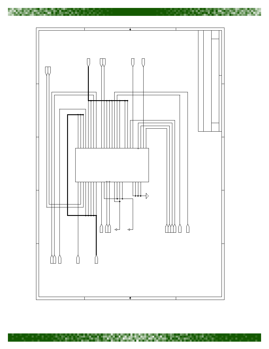
comtech aha corporation
PS4540evb_0405
A subsidiary of Comtech Telecommunications Corporation
Page 21 of 37
5
5
4
4
3
3
2
2
1
1
D
D
C
C
B
B
A
A
CPLD1
AHA4540_EVM
A
CPLD1, Deserializer, SMA or USER Port to UDATA
A
31
9
Friday, March 29, 2002
Title
Siz
e
Document Number
Rev
Date:
Sheet
of
UDATA4
UDATA5
UDATA6
UDATA7
UDATA3
USER_UDATA0
USER_UDATA1
USER_UDATA2
USER_UDATA3
USER_UDATA4
USER_UDATA5
USER_UDATA6
USER_UDATA7
UDATA0
UDATA1
UDATA2
USER_UDATA[7:0]
UDATA[7:0]
VDD_2_5
VDD_3_3
U11
EPM7032V
Package = PLCC44
7
32
38
13
10
22
30
42
4
5
6
8
9
11
12
14
16
17
18
19
20
21
41
40
39
37
36
34
33
31
29
28
27
26
25
24
1
44
2
43
3
15
23
35
I/O(TDI)
I/O(TCK)
I/O(TDO)
I/O(TMS)
GND
GND
GND
GND
I/O
I/O
I/O
I/O
I/O
I/O
I/O
I/O
I/O
I/O
I/O
I/O
I/O
I/O
I/O
I/O
I/O
I/O
I/O
I/O
I/O
I/O
I/O
I/O
I/O
I/O
I/O
I/O
INPUT/GCLRN
INPUT/OE1
INPUT/OE2/GCLK2
INPUT/GCLK1
VCCINT
VCCIO1
VCCINT
VCCIO2
S_UDATA
S_UCLK
CLK_SYNC
UDATA[7:0]
TDI
TM
S
TCK
TDO
USER_UDATA[7:0]
USER_UACPT
USER_URDY
RESETN
UACPT
USER_UCLK
FPGA_PSEL
UECZERO
CLK_SYNC_OUT
BUFOEN1
CHSEL
URDY
UCLK
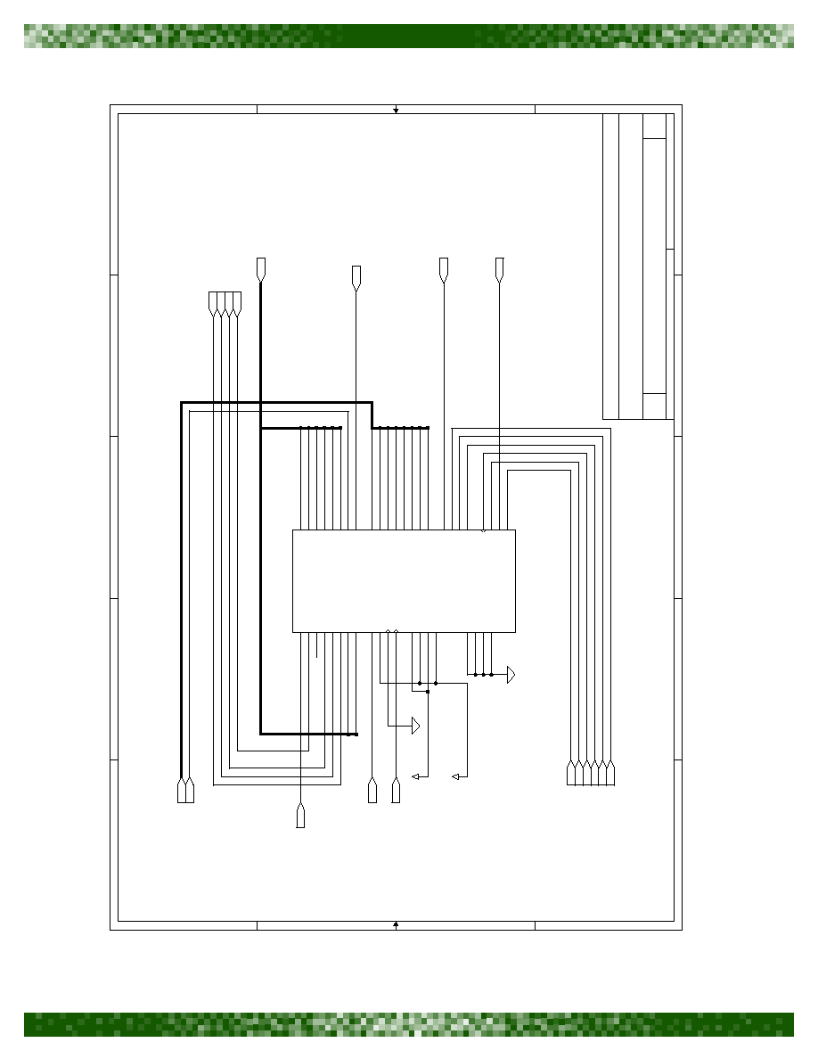
comtech aha corporation
Page 22 of 37
A subsidiary of Comtech Telecommunications Corporation
PS4540evb_0405
5
5
4
4
3
3
2
2
1
1
D
D
C
C
B
B
A
A
CPLD2
<Doc>
A
CPLD2, Serializer, DDATA to SMA
A
41
9
Friday, March 29, 2002
Title
Siz
e
Document Number
Rev
Date:
Sheet
of
USER_DDATA0
USER_DDATA1
USER_DDATA2
USER_DDATA3
USER_DDATA4
USER_DDATA5
USER_DDATA6
USER_DDATA7
USER_DDATA[7:0]
DDATA0
DDATA1
DDATA2
DDATA3
DDATA4
DDATA5
DDATA6
DDATA7
DDATA[7:0]
VDD_2_5
VDD_3_3
U13
EPM7032V
Package = PLCC44
7
32
38
13
10
22
30
42
4
5
6
8
9
11
12
14
16
17
18
19
20
21
41
40
39
37
36
34
33
31
29
28
27
26
25
24
1
44
2
43
3
15
23
35
I/O(TDI)
I/O(TCK)
I/O(TDO)
I/O(TMS)
GND
GND
GND
GND
I/O
I/O
I/O
I/O
I/O
I/O
I/O
I/O
I/O
I/O
I/O
I/O
I/O
I/O
I/O
I/O
I/O
I/O
I/O
I/O
I/O
I/O
I/O
I/O
I/O
I/O
I/O
I/O
INPUT/GCLRN
INPUT/OE1
INPUT/OE2/GCLK2
INPUT/GCLK1
VCCINT
VCCIO1
VCCINT
VCCIO2
DRDY
DCLK
DACPT
S_DDATA
S_DCLK
TDI
TM
S
TCK
TDO
DDATA_[7:0]
BUFOEN2
USER_DDATA[7:0]
RESETN
USER_DRDY
FPGA_PSEL2
SCLK
FPGA_DACPT
USERSEL
USER_DACPT
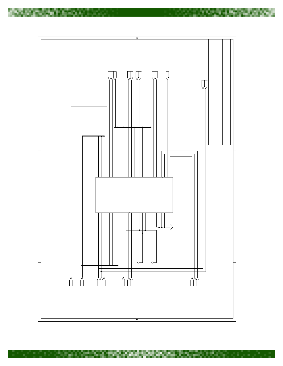
comtech aha corporation
PS4540evb_0405
A subsidiary of Comtech Telecommunications Corporation
Page 23 of 37
5
5
4
4
3
3
2
2
1
1
D
D
C
C
B
B
A
A
CPLD3
<Doc>
A
CPLD3, Serializer, EDATA to SMA
A
51
9
Friday, March 29, 2002
Title
Siz
e
Document Number
Rev
Date:
Sheet
of
EDATA1
EDATA2
EDATA3
EDATA4
EDATA5
EDATA6
EDATA7
USER_EDATA7
USER_EDATA6
USER_EDATA5
USER_EDATA4
USER_EDATA3
USER_EDATA2
USER_EDATA1
USER_EDATA0
USER_EDATA[7:0]
EDATA0
VDD_2_5
VDD_3_3
U14
EPM7032V
Package = PLCC44
7
32
38
13
10
22
30
42
4
5
6
8
9
11
12
14
16
17
18
19
20
21
41
40
39
37
36
34
33
31
29
28
27
26
25
24
1
44
2
43
3
15
23
35
I/O(TDI)
I/O(TCK)
I/O(TDO)
I/O(TMS)
GND
GND
GND
GND
I/O
I/O
I/O
I/O
I/O
I/O
I/O
I/O
I/O
I/O
I/O
I/O
I/O
I/O
I/O
I/O
I/O
I/O
I/O
I/O
I/O
I/O
I/O
I/O
I/O
I/O
I/O
I/O
INPUT/GCLRN
INPUT/OE1
INPUT/OE2/GCLK2
INPUT/GCLK1
VCCINT
VCCIO1
VCCINT
VCCIO2
TCK
TM
S
TDO
TDI
EDATA[7:0]
ERDY
EACPT
ECLK
EEND
S_EDATA
S_ECLK
BUFOEN3
CSCLK
VSCLK
RESETN
USER_EDATA[7:0]
CHSEL
USER_ERDY
ENC_CHANNEL_CLK
EST
A
R
T
USER_EEND
USER_ESTART
T
EST
1
0

comtech aha corporation
Page 24 of 37
A subsidiary of Comtech Telecommunications Corporation
PS4540evb_0405
5
5
4
4
3
3
2
2
1
1
D
D
C
C
B
B
A
A
CPLD4
Package = HG-8002JA
Place all 70 ohm resistors
near CPLD4 on the approp
riate
pin.
<Doc>
A
CPLD4, Deserializer, Serial input to 8-bit data
A
61
9
Friday, March 29, 2002
Title
Siz
e
Document Number
Rev
Date:
Sheet
of
CSDATA1
CSDATA4
CSDATA2
CSDATA3
CSDATA0
CSDATA5
CSDATA6
CSDATA7
CSDATA[7:0]
VDD_2_5
VDD_3_3
VDD_3_3
R41
70
R42
70
R44
70
U15
EPM7032V
Package = PLCC44
7
32
38
13
10
22
30
42
4
5
6
8
9
11
12
14
16
17
18
19
20
21
41
40
39
37
36
34
33
31
29
28
27
26
25
24
1
44
2
43
3
15
23
35
I/O(TDI)
I/O(TCK)
I/O(TDO)
I/O(TMS)
GND
GND
GND
GND
I/O
I/O
I/O
I/O
I/O
I/O
I/O
I/O
I/O
I/O
I/O
I/O
I/O
I/O
I/O
I/O
I/O
I/O
I/O
I/O
I/O
I/O
I/O
I/O
I/O
I/O
I/O
I/O
INPUT/GCLRN
INPUT/OE1
INPUT/OE2/GCLK2
INPUT/GCLK1
VCCINT
VCCIO1
VCCINT
VCCIO2
R40
70
Y1
OSC86M0
4
3
2
1
VCC
OUT
GND
EN
R43
70
S_CDATA
CPCLK_SER
TCK
TM
S
TDO
TDI
EPCLK
FPGA_PSEL4
RESETN
S_CCLK
CSDATA[7:0]
DPCLK
CLK_43M0
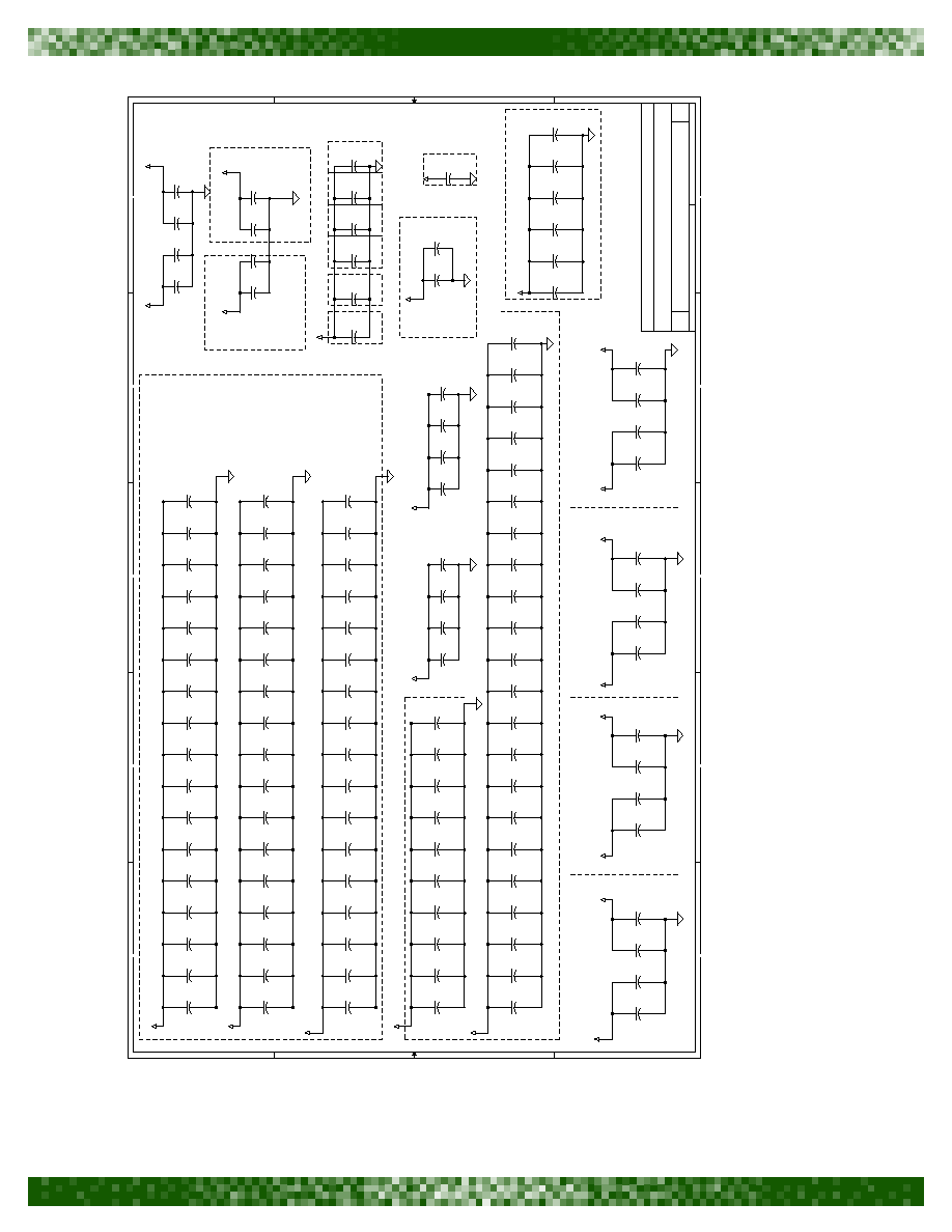
comtech aha corporation
PS4540evb_0405
A subsidiary of Comtech Telecommunications Corporation
Page 25 of 37
5
5
4
4
3
3
2
2
1
1
D
D
C
C
B
B
A
A
AHA4540 Devi
c
e
XILINX FPG
A
Device
CPLD1
CPLD2
CPLD3
CPLD4
Miscellaneou
s
DECOUPLING
CAPS
BOTH
OP283
AGND
U3A & U17
A
U4 & U8
BOTH
MAX997
SN74LVT12
5
U5
U6
U12
U19
U18
U16
MAX3221
BOTH
JTOS-300
U2 & U7
AGND
SPROM 18V0
4
U10
AD9851, U2
0
AD9851, U
2
1
<Doc>
A
Decoupling Caps
B
71
9
Friday, March 29, 2002
Ti
t
l
e
S
i
z
e
Document Number
Rev
Date:
Sheet
of
VDD_3_3
VDD_1_8
VDD_1_8
VDD_3_3
VDD_3_3
VDD_2_5
VDD_3_3
VDD_2_5
VDD_3_3
VDD_2_5
VDD_3_3
VDD_2_5
VDD_3_3
VDD_1_8
VDD_1_8
ANALOG
_
1
6
VDD_3_3
VDD_3_3
VDD_3_3
ANALOG
_
1
2
VDD_3_3
VDD_5_0
VDD_5_0
C9
0.1uF
C10
0.1uF
C11
0.1uF
C12
0.1uF
C13
0.1uF
C14
0.1uF
C15
0.1uF
C16
0.1uF
C17
0.1uF
C18
0.1uF
C99
0.1uF
C97
0.1uF
C98
0.1uF
C96
0.1uF
C103
0.1uF
C101
0.1uF
C102
0.1uF
C20
0.1uF
C19
0.1uF
C100
0.1uF
C24
0.1uF
C23
0.1uF
C22
0.1uF
C21
0.1uF
C107
0.1uF
C105
0.1uF
C106
0.1uF
C104
0.1uF
C185
0.1uF
C182
0.1uF
C184
0.1uF
C183
0.1uF
C111
0.1uF
C109
0.1uF
C110
0.1uF
C108
0.1uF
C25
0.1uF
C31
0.1uF
C29
0.1uF
C30
0.1uF
C35
0.1uF
C34
0.1uF
C33
0.1uF
C27
0.1uF
C28
0.1uF
C26
0.1uF
C32
0.1uF
C39
0.1uF
C38
0.1uF
C37
0.1uF
C36
0.1uF
C43
0.1uF
C42
0.1uF
C44
0.1uF
C45
0.1uF
C40
0.1uF
C41
0.1uF
C46
0.1uF
C145
0.1uF
C48
0.1uF
C47
0.1uF
C52
0.1uF
C51
0.1uF
C50
0.1uF
C49
0.1uF
C189
0.1uF
C186
0.1uF
C188
0.1uF
C187
0.1uF
C56
0.1uF
C55
0.1uF
C54
0.1uF
C53
0.1uF
C60
0.1uF
C59
0.1uF
C61
0.1uF
C62
0.1uF
C141
0.1uF
C140
0.1uF
C57
0.1uF
C58
0.1uF
C63
0.1uF
C142
0.1uF
C137
0.1uF
C139
0.1uF
C138
0.1uF
C143
0.1uF
C144
0.1uF
C64
0.1uF
C65
0.1uF
C66
0.1uF
C67
0.1uF
C68
0.1uF
C69
0.1uF
C70
0.1uF
C71
0.1uF
C72
0.1uF
C73
0.1uF
C75
0.1uF
C77
0.1uF
C83
0.1uF
C79
0.1uF
C74
0.1uF
C76
0.1uF
C82
0.1uF
C80
0.1uF
C78
0.1uF
C81
0.1uF
C147
0.1uF
C146
0.1uF
C151
0.1uF
C150
0.1uF
C149
0.1uF
C148
0.1uF
C85
0.1uF
C87
0.1uF
C93
0.1uF
C89
0.1uF
C84
0.1uF
C86
0.1uF
C92
0.1uF
C90
0.1uF
C88
0.1uF
C91
0.1uF
C136
0.1uF
C133
0.1uF
C135
0.1uF
C134
0.1uF
C95
0.1uF
C94
0.1uF
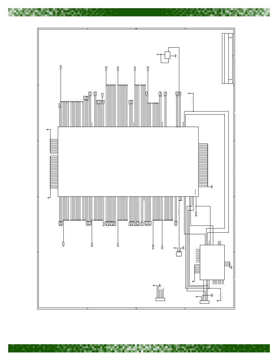
comtech aha corporation
Page 26 of 37
A subsidiary of Comtech Telecommunications Corporation
PS4540evb_0405
5
5
4
4
3
3
2
2
1
1
D
D
C
C
B
B
A
A
LOAD PROGRAM
FROM PC
PARALLEL PORT
CABLE
LOAD PROGRAM
F
R
O
M
PROM
JTAG fo
r
SPROM an
d
FPGA
FPGA PGM
CABLE
Note: U7 (SPROM) is socketed
,
surface mount
socket with locat
ing pins.
FPGA
Package = HG-
8002JA
<Doc>
<RevCode>
FPGA
C
81
9
Friday, March 29, 2002
Title
Size
Document Number
Rev
Date:
S
heet
of
DDATA4
USER_CDATA11
LEDN5
CDATA9
CDATA6
DDATA[7:0]
DDATA5
USER_CDATA6
MA
4
MA
0
LEDN6
EDATA7
CDATA8
MDATA[7:0]
CDATA[15:0]
USER_CDATA15
EDATA4
CDATA10
USER_CDATA1
MDATA4
MDATA3
MA
1
CSDATA6
CDATA4
LEDN4
USER_CDATA7
MDATA0
MA
5
CSDATA5
CDATA3
LEDN7
LEDN2
CSDATA2
MA[6:0]
DDATA0
USER_CDATA3
MDATA6
CSDATA1
EDATA6
CDATA5
USER_CDATA9
USER_CDATA13
MA
2
CDATA13
CDATA11
MDATA5
LEDN3
DDATA7
DDATA3
DDATA1
LEDN1
LEDN0
MA
6
EDATA5
EDATA2
EDATA1
CDATA14
CDATA0
LEDN[7:0]
USER_CDATA14
DDATA6
USER_CDATA12
CDATA12
USER_CDATA4
USER_CDATA0
MDATA7
MDATA2
CSDATA4
CDATA1
USER_CDATA10
MA
3
CSDATA7
EDATA[7:0]
CSDATA[7:0]
USER_ROTATE
CSDATA0
CDATA15
DDATA2
USER_CDATA2
USER_CDATA8
LOAD_PGMN
MDATA1
CSDATA3
EDATA3
EDATA0
CDATA7
CDATA2
DIN
PGM_CCLK
PGM_CCLK
DIN
DONE
DONE
LOAD_PGMN
USER_CDATA[15:0]
CLK_3M686
4
FSDATA[7:0]
FSDATA2
FSDATA3
FSDATA1
FSDATA0
FSDATA4
FSDATA5
FSDATA6
FSDATA7
USER_CDATA5
TEST[7:0]
TEST2
TEST3
TEST1
TEST0
TEST4
TEST5
TEST6
TEST7
VDD_1_8
VDD_3_3
VDD_3_3
VDD_3_3
VDD_3_3
VDD_3_3
VDD_3_3
VDD_3_3
VDD_3_3
U10
18V0
4
Package = PLCC44
9
11
13
5
2
21
27
16
37
19
23
41
44
14
22
32
42
3
12
24
34
1
4
6
7
10
15
17
18
20
25
26
28
29
30
31
33
35
36
38
39
40
43
TDI
TMS
TCK
CLK
D0
CEN
CEON
CFN
TDO
RESETN
VCC
VCC
VCC
VCCO
VCCO
VCCO
VCCO
GND
GND
GND
GND
NC
NC
NC
NC
NC
NC
NC
NC
NC
NC
NC
NC
NC
NC
NC
NC
NC
NC
NC
NC
NC
NC
R26
390
Y2
OSC3M686
4
4
3
2
1
VCC
OUT
GND
EN
J11
CON6
Package = TH_STP_HDR_6
1
2
3
4
5
6
U9
XCV200E-8PQ24
0C
Package = PQ240
15
25
30
44
55
61
76
85
90
105
116
121
136
146
150
165
3
4
5
6
7
9
10
11
12
13
17
18
19
20
21
23
24
26
27
28
31
33
34
35
36
38
39
40
41
42
46
47
48
49
50
52
53
54
56
57
63
64
58
62
65
66
67
68
70
71
72
73
74
78
79
80
81
82
84
86
94
95
96
97
99
100
101
102
103
107
108
109
110
111
113
114
115
117
118
124
125
122
60
239
178
210
213
202
203
205
206
208
216
217
171
173
174
175
186
187
188
189
160
161
162
163
167
168
169
170
149
152
153
154
155
156
157
159
126
127
128
130
131
132
133
134
138
139
140
141
142
144
145
147
191
192
193
194
195
199
200
201
218
220
221
222
223
224
228
229
230
234
235
236
237
231
238
2
183
177
120
89
92
14
22
29
37
45
51
59
69
75
83
91
98
106
112
119
129
135
143
151
158
166
172
179
8
1
181
182
190
196
204
211
219
227
233
176
180
197
207
212
226
232
240
16
32
43
77
88
104
137
148
164
198
214
123
87
93
209
215
184
185
VCCO
VCCO
VCCO
VCCO
VCCO
VCCO
VCCO
VCCO
VCCO
VCCO
VCCO
VCCO
VCCO
VCCO
VCCO
VCCO
I/O
I/O
I/O_VREF
I/O
I/O
I/O_VREF
I/O_
I/O
I/O_VREF
I/O
I/O
I/O
I/O
I/O
I/O
I/O_VREF
I/O
I/O
I/O
I/O
I/O
I/O
I/O
I/O
I/O_VREF
I/O
I/O
I/O
I/O
I/O
I/O
I/O_VREF
I/O
I/O
I/O_VREF
I/O
I/O
I/O
I/O
I/O
I/O
I/O
M1
M2
I/O
I/O_VREF
I/O
I/O
I/O_VREF
I/O
I/O
I/O_VREF
I/O
I/O
I/O
I/O
I/O
I/O
I/O_VREF
I/O
I/O
I/O
I/O
I/O_VREF
I/O
I/O
I/O
I/O
I/O
I/O
I/O_VREF
I/O
I/O
I/O_VREF
I/O
I/O
I/O_VREF
I/O
I/O
I/O
I/O
PROGRAM
M0
TCK
I/O_DOUT_BUSY
GCK2
GCK3
I/O
I/O
I/O_VREF
I/O
I/O
I/O_VREF
I/O
I/O_VREF
I/O
I/O
I/O_VREF
I/O
I/O_VREF
I/O
I/O
I/O
I/O
I/O
I/O
I/O
I/O_VREF
I/O
I/O
I/O
I/O
I/O
I/O
I/O
I/O
I/O_VREF
I/O
I/O_VREF
I/O
I/O
I/O
I/O
I/O
I/O_VREF
I/O
I/O
I/O
I/O
I/O
I/O
I/O_VREF
I/O
I/O_VREF
I/O_VREF
I/O
I/O
I/O_VREF
I/O
I/O
I/O
I/O
I/O_VREF
I/O
I/O
I/O
I/O
I/O
I/O
I/O_VREF
I/O
I/O
I/O
I/O_VREF
I/O
I/O_VREF
I/O
TMS
TDI
D0/DIN(I/O)
DONE
GCK1
GCK0
GND
GND
GND
GND
GND
GND
GND
GND
GND
GND
GND
GND
GND
GND
GND
GND
GND
GND
GND
GND
GND
GND
CCLK
GND
GND
TDO
GND
GND
GND
GND
GND
GND
GND
GND
VCCO
VCCO
VCCO
VCCO
VCCO
VCCO
VCCO
VCCO
VCCINT
VCCINT
VCCINT
VCCINT
VCCINT
VCCINT
VCCINT
VCCINT
VCCINT
VCCINT
VCCINT
I/O_INIT
I/O
I/O
I/O
I/O
I/O_CS
I/O_WRITE
R27
4.7K
JP1
HEADER_3
Package = TH_STP_HDR_3
1
2
3
J12
CON6
Package = TH_STP_HDR_6
1
2
3
4
5
6
R25
3.3K
MDATA[7:0]
ROUT
LEDN[7:0]
DDATA[7:0]
DRDY
CSDATA[7:0]
EDATA[7:0]
CDATA[15:0]
PSEL2
PSEL1
ECLK
USERSEL
UCLKADJ2
GOUT0
GOUT1
INVALIDN
RESETN
DCLKADJ2
DCLK
TXIN
CLSB
CRDY
CSTART
CACPT
PSEL4
LOAD_PGMN
ROTATE
RS232EN
MRDY_DTACKN
MWRN_RWN
MRDN_DSN
MCSN
PROCMODE
MUXMO
D
E
USER_ROTATE
USER_CACPT
USER_CLSB
USER_CSTART
USER_CRDY
EACPT
ERDY
FPGA_DACPT
MA[6:0]
CHSEL
UECZERO
SW1
SW2
SW3
CPLD3_EACPT
USER_EACPT
MA
LE
USER_CDATA[15:0]
CPCLK_SER
CCLK
MINTN
USER_ROTATE
USER_CPCLK
CLK_43M0
ENC_CHANNEL_CLK
ENC_PAYLOAD_CLK
DEC_CHANNEL_CLK
DEC_PAYLOAD_CLK
FSDATA[7:0]
FQ_UD_ENC
WLOAD_ENC
FQ_UD_DEC
WLOAD_DEC
RESET_AD9851
TEST[7:0]
RESET_CPLD
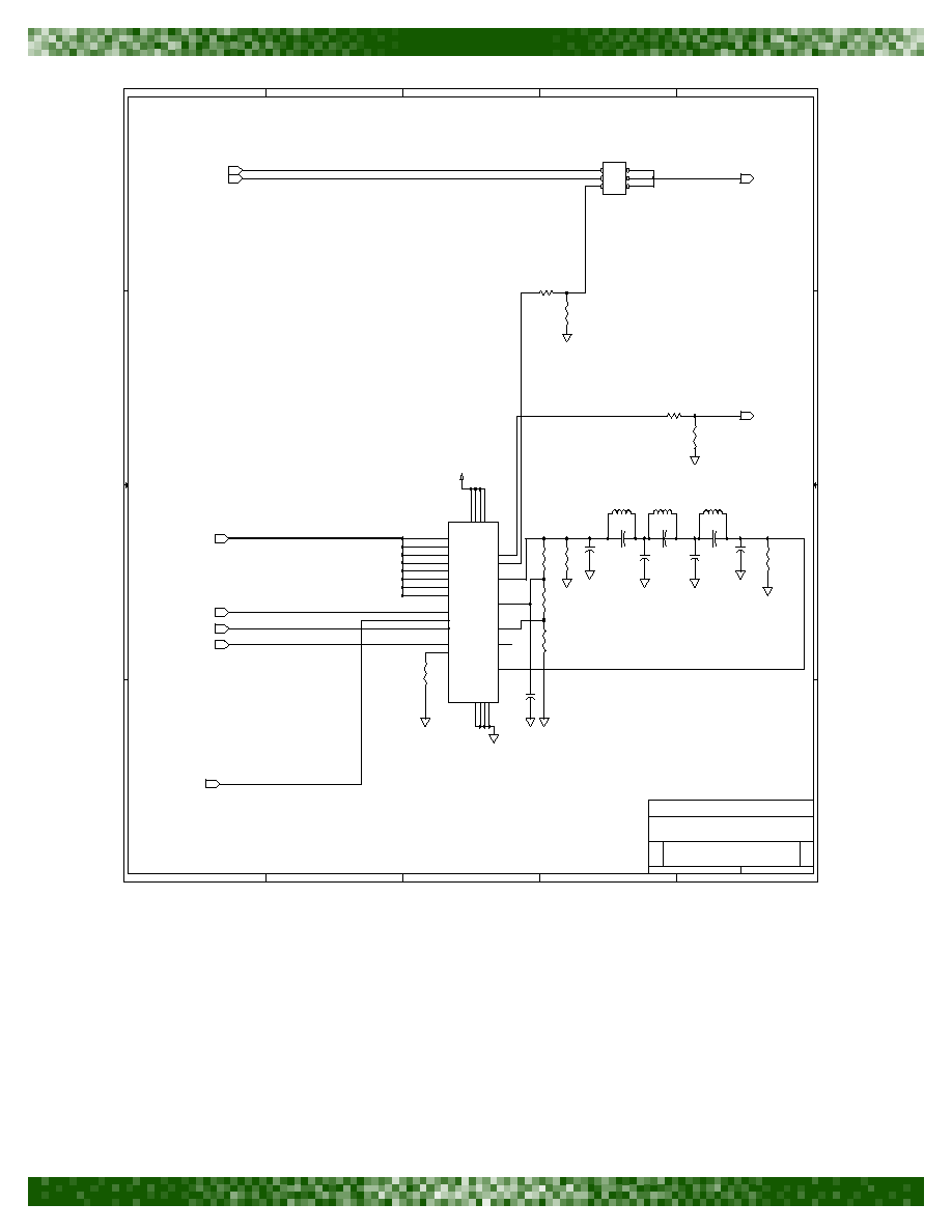
comtech aha corporation
PS4540evb_0405
A subsidiary of Comtech Telecommunications Corporation
Page 27 of 37
5
5
4
4
3
3
2
2
1
1
D
D
C
C
B
B
A
A
AHA4524_EVB
D
FREQUENCY SYNTH DECODER
B
9
19
Friday, March 29, 2002
Title
Size
Document Number
Rev
Date:
Sheet
of
D7
D6
D5
D4
D3
D2
D1
D0
VDD_5_0
R51
70
R50
33
R95
3.9K
U20
AD9851
9
7
4
3
2
1
28
27
26
25
8
14
13
12
17
21
20
15
16
22
6
23
11
18
5
24
10
19
CLKIN
W_CLK
D0
D1
D2
D3
D4
D5
D6
D7
FQ_UD
QOUT
QOUTB
RSET
DACBL(NC)
IOUT
IOUTB
VINN
VINP
RESET
DVDD
DVDD
AVDD
AVDD
DGND
DGND
AG
ND
AG
ND
C167
470pF
C164
33pF
C166
22pF
R92
200
R91
200
C161
5.6pF
C163
22pF
C160
1pF
R90
100K
R94
100
R93
100K
L2
390nH
L1
470nH
C165
22pF
C162
4.7pF
L3
390nH
R52
33
R53
70
JP8
HEADER 3X2
1
2
3
4
5
6
WLOAD
RESET_AD9851
FQ_UD
D[7:0]
CLK_SYNC
VSCLK
DEC_PAYLOAD_CLK
S_DCLK_IN
CLK_30M0
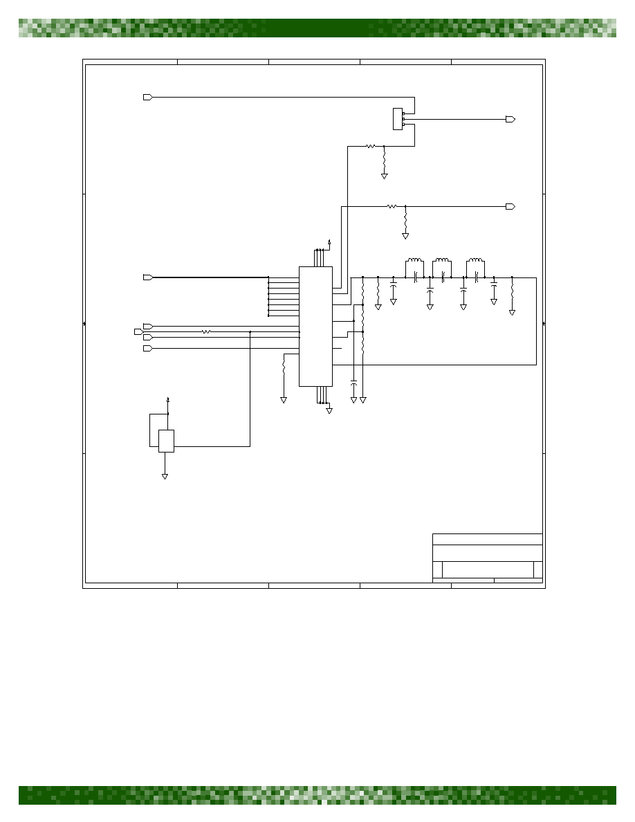
comtech aha corporation
Page 28 of 37
A subsidiary of Comtech Telecommunications Corporation
PS4540evb_0405
5
5
4
4
3
3
2
2
1
1
D
D
C
C
B
B
A
A
Place Oscillator
near
U21.9.
Place resistor
near
U21.9.
AHA4524_EVB
D
FREQUENCY SYNTH ENCODER
B
10
19
Friday, March 29, 2002
Title
Size
Document Number
Rev
Date:
Sheet
of
D7
D6
D5
D4
D3
D2
D1
D0
VDD_5_0
VDD_5_0
U21
AD9851
9
7
4
3
2
1
28
27
26
25
8
14
13
12
17
21
20
15
16
22
6
23
11
18
5
24
10
19
CLKIN
W_CLK
D0
D1
D2
D3
D4
D5
D6
D7
FQ_UD
QOUT
QOUTB
RSET
DACBL(NC)
IOUT
IOUTB
VINN
VINP
RESET
DVDD
DVDD
AVDD
AVDD
DGND
DGND
AG
ND
AG
ND
R102
3.9K
C176
470pF
C173
33pF
Y3
OSC30M0
4
3
2
1
VCC
OUT
GND
EN
C175
22pF
R99
200
C170
5.6pF
C172
22pF
R98
200
R49
70
C169
1pF
R97
100K
R101
100
R48
33
R100
100K
L6
390nH
L5
470nH
C174
22pF
C171
4.7pF
L7
390nH
R54
33
R55
70
JP7
HEADER_3
Package = TH_STP_HDR_3
1
2
3
R47
51
WLOAD
RESET_AD9851
CLK_SYNC
D[7:0]
VSCLK
ENC_PAYLOAD_CLK
FQ_UD
CLK_30M0
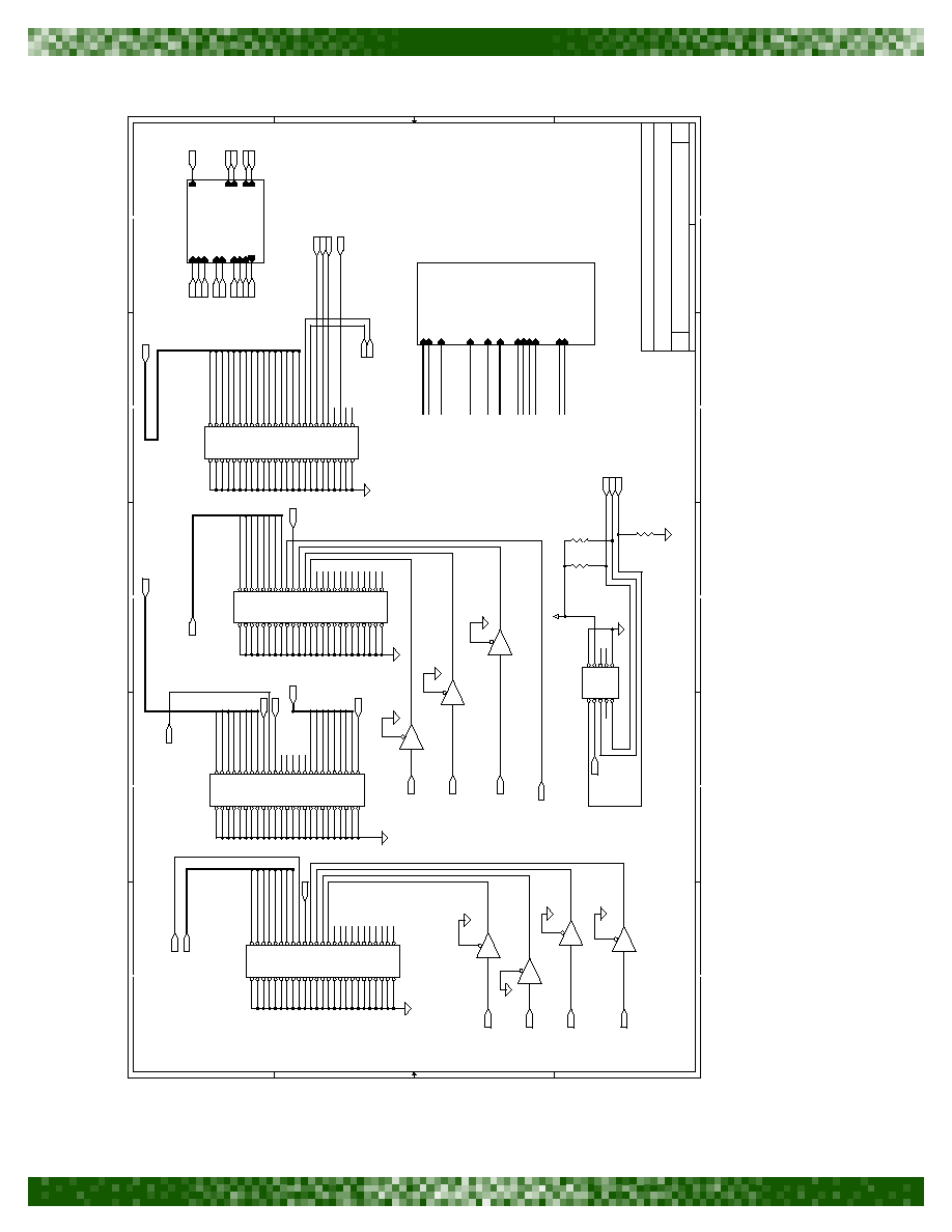
comtech aha corporation
PS4540evb_0405
A subsidiary of Comtech Telecommunications Corporation
Page 29 of 37
5
5
4
4
3
3
2
2
1
1
D
D
C
C
B
B
A
A
JTAG POR
T
In Syste
m
Programmi
n
g
of CPLD
s
Decoded Data
O
u
t
Encoded Data
O
u
t
Channel Data
I
n
I/O CONN
Unencoded Data
I
n
<Doc>
A
I/O_CONN, USER Interface Connectors
B
11
19
Friday, March 29, 2002
Ti
t
l
e
S
i
z
e
Document Number
Rev
Date:
Sheet
of
RES_
TERM
RES_
TERM
USER_UDATA[7:0]
USER_URDY
USER_UCLK
USER_
E
A
C
P
T
USER_ECL
K
USER_CDATA[15:0]
USER_CRDY
USER_CLS
B
USER_
C
S
T
A
R
T
USER_CPCLK
USER_DA
C
P
T
USER_DCLK
SM
A
SM
A
S_
EDATA
S_EC
L
K
CLK_SYNC_OUT
BUFOEN1
S_DD
A
T
A
S_DCLK
BUFOEN2
S_UDATA
S_UCLK
S_CDATA
S_CCLK
BUFOEN3
CSCLK
S_DCLK_IN
USER_DD
A
T
A
0
USER_DD
A
T
A
1
USER_DD
A
T
A
2
USER_DD
A
T
A
3
USER_DD
A
T
A
4
USER_DD
A
T
A
5
USER_DD
A
T
A
6
USER_DD
A
T
A
7
USER_DDATA[7:0]
USER_
E
D
A
T
A
0
USER_
E
D
A
T
A
1
USER_
E
D
A
T
A
2
USER_
E
D
A
T
A
3
USER_
E
D
A
T
A
4
USER_
E
D
A
T
A
5
USER_
E
D
A
T
A
6
USER_
E
D
A
T
A
7
USER_EDATA[7:
0
]
USER_CRDY
USER_CLS
B
USER
_
C
S
T
A
R
T
USER_DEND
USER_DERR
USER_DRDY
USER_DA
C
P
T
USER_CPCLK
USER_CDA
T
A
6
USER_CDATA[15:0]
USER_CDA
T
A
0
USER_CDA
T
A
1
4
USER_CDA
T
A
4
USER_CDA
T
A
1
2
USER_CDA
T
A
5
USER_CDA
T
A
1
USER_CDA
T
A
9
USER_CDA
T
A
1
3
USER_CDA
T
A
3
USER_CDA
T
A
2
USER_CDA
T
A
1
1
USER_CDA
T
A
1
5
USER_CDA
T
A
7
USER_CDA
T
A
8
USER_CDA
T
A
1
0
USER_DCLK
U
S
E
R_
ROT
AT
E
USER_CA
C
P
T
USER_ECL
K
USER_DSTART
USER_UDA
T
A
5
USER_URDY
USER_UDA
T
A
3
USER_UDA
T
A
1
USER_UCLK
USER_UDA
T
A
0
USER_UDA
T
A
4
USER_UACP
T
USER_UDA
T
A
6
USER_UDA
T
A
2
USER_UDATA[7:0]
USER_CDATA[15:0]
USER_URDY
USER_UCLK
USER
_
E
A
C
P
T
USER_ECL
K
USER_CRDY
USER_CLS
B
USER
_
C
S
T
A
R
T
USER_CPCL
K
USER_D
A
C
P
T
USER_DCLK
USER_UDATA[7:0]
USER_UDA
T
A
7
USER_ERDY
USER_EEND
U
S
ER_
ESTART
TES
T
1
0
TEST3
TEST5
TEST2
TEST7
TEST4
TEST6
TEST1
TEST0
VDD_3_3
JP4
HEADE
R
_25X
2
Package = TH_WLD_HDR_25X
2
12
34
56
78
91
0
11
12
13
14
15
16
17
18
19
20
21
22
23
24
25
26
27
28
29
30
31
32
33
34
35
36
37
38
39
40
41
42
43
44
45
46
47
48
49
50
JP2
HEADE
R
_25X
2
Package = TH_WLD_HDR_25X
2
12
34
56
78
91
0
11
12
13
14
15
16
17
18
19
20
21
22
23
24
25
26
27
28
29
30
31
32
33
34
35
36
37
38
39
40
41
42
43
44
45
46
47
48
49
50
JP5
HEAD
E
R
_25X
2
Package = TH_WLD_HDR_25X
2
12
34
56
78
91
0
11
12
13
14
15
16
17
18
19
20
21
22
23
24
25
26
27
28
29
30
31
32
33
34
35
36
37
38
39
40
41
42
43
44
45
46
47
48
49
50
JP3
HEAD
E
R
_25X
2
Package = TH_WLD_HDR_25X
2
12
34
56
78
91
0
11
12
13
14
15
16
17
18
19
20
21
22
23
24
25
26
27
28
29
30
31
32
33
34
35
36
37
38
39
40
41
42
43
44
45
46
47
48
49
50
U19A
SN74L
V
T
1
2
5
Package = SMD
2
3
1
U18A
SN74L
V
T
1
2
5
Package = SMD
2
3
1
U19B
SN74L
V
T
1
2
5
Package = SMD
5
6
4
JP6
HEADE
R
_
5
X
2
12
34
56
78
91
0
U19C
SN74
L
V
T
1
2
5
Package = SMD
9
8
10
U18B
SN74L
V
T
1
2
5
Package = SMD
5
6
4
U18C
SN74L
V
T
1
2
5
Package = SMD
9
8
10
R62
1K
R63
1K
R64
1K
U19D
SN74L
V
T
1
2
5
Package = SMD
12
11
13
TDI
TM
S
TC
K
TD
O
USER_DDATA[7:0]
USER_EDATA[7:
0
]
USER_CRDY
USER_
C
S
T
A
R
T
USER_CLS
B
BUFOEN1
CLK_SYNC_OUT
BUFOEN2
S_DD
A
T
A
S_DCLK
USER_CDATA[15:0]
DERR
DEND
DST
ART
DCLK
USER_DRDY
USER_DA
C
P
T
S_
EDATA
S_EC
L
K
BUFOEN3
USER_CPCLK
USER_EEND
U
S
ER_
ESTART
USER_
E
A
C
P
T
U
S
ER_
RO
TATE
USER_CA
C
P
T
ECLK
S_DCLK_IN
USER_UDATA[7:0]
USER_UCLK
USER_URDY
USER_UA
C
P
T
S_UCLK
S_UD
A
T
A
S_CCLK
S_CD
A
T
A
CSCLK
USER_ERDY
TES
T
1
0
TEST[
7
:
0
]
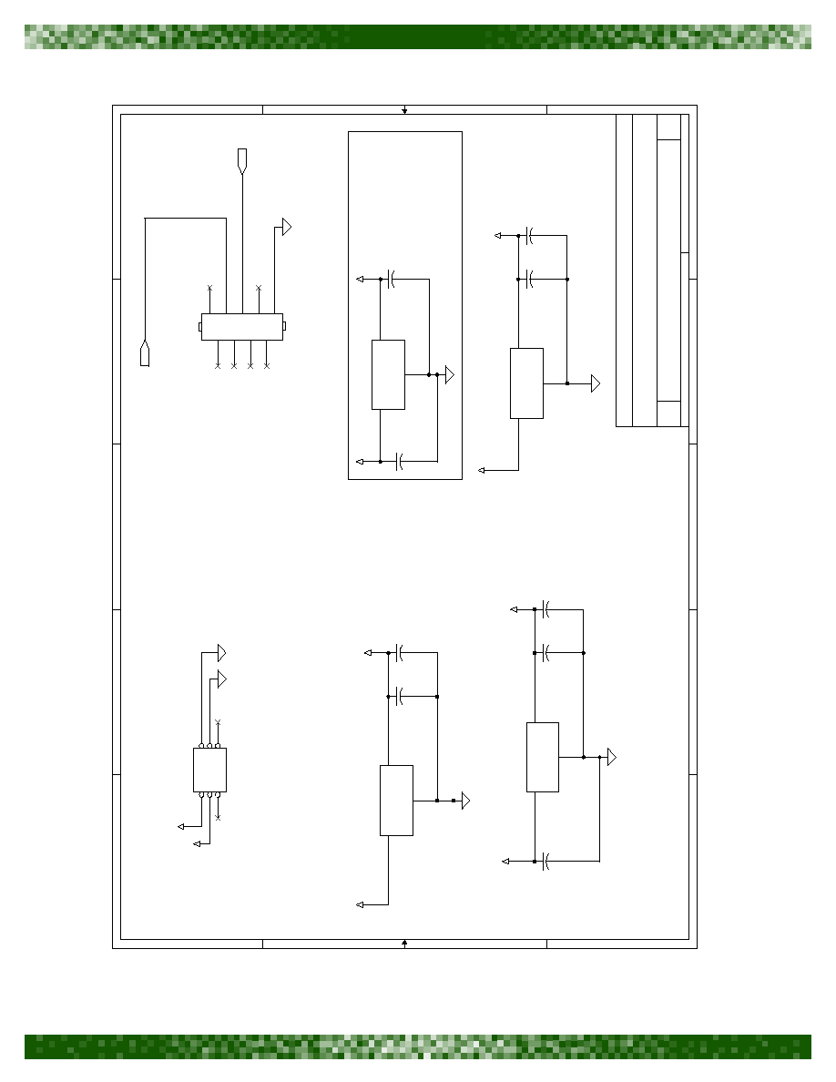
comtech aha corporation
Page 30 of 37
A subsidiary of Comtech Telecommunications Corporation
PS4540evb_0405
5
5
4
4
3
3
2
2
1
1
D
D
C
C
B
B
A
A
Note:
1. PCB board should have large
pad for TAB
AGND
PC I/O, Pow
e
r
TANTALUM
TANTALUM
AGND
TAB AREA = 1000mm^2
TAB AREA = TAB AREA
TANTALUM
Put on bottom side
if top side too full
TANTALUM
TANTALUM
TANTALUM
TAB AREA = TAB AREA
TAB AREA = TAB AREA
GND_SIGNAL
AHA4540_EVB
A
PC I/O, Power
A
13
19
Friday, March 29, 2002
Title
Siz
e
Document Number
Rev
Date:
Sheet
of
VDD_2_5
ANALOG_12
VDD_5_0
ANALOG_16
VDD_1_8
VDD_5_0
VDD_3_3
VDD_5_0
VDD_5_0
ANALOG_16
C113
22uF
C177
22uF
PCB Footprint = D
REG4
MIC29300-3.3BU
Package = TO_263_3
1
2
3
IN
GND
OUT
C178
22uF
JDR1
RS232
Package = RtAn_9Pin_DSUB
5
9
4
8
3
7
2
6
1
5
9
4
8
3
7
2
6
1
C181
10uF
PCB Footprint = X
REG3
MIC39300-1.8BU
Package = TO_263_3
1
2
3
IN
GND
OUT
C179
22uF
PCB Footprint = D
REG2
MIC29150-12BU
Package = TO_263_3
1
2
3
IN
GND
OUT
REG1
MIC39300-2.5BU
Package = TO_263_3
1
2
3
IN
GND
OUT
C180
22uF
C132
22uF
C114
10uF
JP9
HEADER 3X2
12
34
56
C131
10uF
TX
O
U
T
RIN
comtech aha corporation
PS4540evb_0405
A subsidiary of Comtech Telecommunications Corporation
Page 31 of 37
5
5
4
4
3
3
2
2
1
1
D
D
C
C
B
B
A
A
<Doc>
A
Resistor Terminations, LVPECL
B
14
19
Friday, March 29, 2002
Title
Size
Document Number
Rev
Date:
Sheet
of
USER_UCLK
USER_ECLK
USER_CRDY
USER_CLSB
USER_CSTART
USER_CPCLK
USER_DCLK
USER_URDY
USER_
CDAT
A
3
USER_
CDAT
A
4
USER_
CDAT
A5
USER_
CDAT
A
6
USER_
CDAT
A7
USER_
CDAT
A
8
USER_
CDAT
A
9
USER_
CDAT
A1
0
USER_
CDAT
A
1
1
USER_
CDAT
A1
2
USER_
CDAT
A1
3
USER_
CDAT
A
1
4
USER_
CDAT
A
1
USER_
CDAT
A2
USER_
CDAT
A0
USER_
UDAT
A
0
USER_
UDAT
A1
USER_UDATA[7:0]
USER_
UDAT
A
7
USER_
UDAT
A
5
USER_
UDAT
A
2
USER_
UDAT
A
3
USER_
UDAT
A
4
USER_
UDAT
A
6
USER_CDATA[15:0]
USER_
CDAT
A
1
5
USER_EACPT
R134
51
R107
51
R108
51
R109
51
R110
51
R111
51
R114
51
R113
51
R112
51
R115
51
R160
51
R161
51
R105
51
R121
51
R118
51
51
R123
51
R122
51
R117
51
R116
51
R138
51
R126
51
R127
51
R129
51
R128
51
R130
51
R135
51
R46
51
R125
51
R124
51
R132
51
R133
51
R131
51
R45
51
USER_UDATA[7:0]
USER_URDY
USER_UCLK
USER_EACPT
USER_ECLK
USER_CRDY
USER_CLSB
USER_CSTART
USER_DCLK
USER_DACPT
USER_CPCLK
USER_CDATA[15:0]

comtech aha corporation
Page 32 of 37
A subsidiary of Comtech Telecommunications Corporation
PS4540evb_0405
5
5
4
4
3
3
2
2
1
1
D
D
C
C
B
B
A
A
RS232 interface
<Doc>
A
RS232 interface
A
15
19
Friday, March 29, 2002
Title
Siz
e
Document Number
Rev
Date:
Sheet
of
VDD_3_3
VDD_3_3
U16
M
A
X
3221
Package = SSOP16
8
11
14
15
9
10
13
2
4
5
6
12
16
3
7
1
RIN
TIN
GND
VCC
ROUT
INVALID
TOUT
C1+
C1-
C2+
C2-
FORCEON
FORCEOFF
V+
V-
EN
C119
0.1uF
C120
0.1uF
R69
1K
C121
0.1uF
C122
0.1uF
TXIN
RIN
RS232EN
TX
O
U
T
ROUT
INVALIDN
comtech aha corporation
PS4540evb_0405
A subsidiary of Comtech Telecommunications Corporation
Page 33 of 37
5
5
4
4
3
3
2
2
1
1
D
D
C
C
B
B
A
A
USER_CLK_SY
N
C
S_DDATA
S_DCLK
S_EDATA
S_ECLK
SMA
Route Data and Cl
ock for each
interface toget
her. (Same
Length Tr
aces)
Place 51 ohm res
istors near
components at the
receiving
end of the trace
,
not near
SMA conne
ctor.
Place all SN74LVT125
buffers inline with the
SMA connector and the IC
they go to. Including
buffers on IO_CONN page.
<Doc>
A
SM
A
B
16
19
Friday, March 29, 2002
Ti
t
l
e
S
i
z
e
Document Number
Rev
Date:
Sheet
of
R15
51
J9
SM
A
1
2
U5A
SN74
L
V
T
1
2
5
Package = SMD
2
3
1
U6A
SN74
L
V
T
1
2
5
Package = SMD
2
3
1
U6B
SN74
L
V
T
1
2
5
Package = SMD
5
6
4
J13
SM
A
1
2
R11
51
J1
SM
A
1
2
R104
51
J6
SM
A
1
2
J4
SM
A
1
2
U12B
SN74L
V
T
1
2
5
Package = SMD
5
6
4
U12A
SN74L
V
T
1
2
5
Package = SMD
2
3
1
J10
SM
A
1
2
J8
SM
A
1
2
J2
SM
A
1
2
R13
51
R14
51
J5
SM
A
1
2
J7
SM
A
1
2
R12
51
J3
SM
A
1
2
S_DD
A
T
A
S_DCLK
BUFOEN1
BUFOEN2
S_
EDATA
S_EC
L
K
CLK_SYNC_OUT
S_CD
A
T
A
S_CCLK
S_UD
A
T
A
S_UCLK
BUFOEN3
CSCLK
S_DCLK_IN
comtech aha corporation
Page 34 of 37
A subsidiary of Comtech Telecommunications Corporation
PS4540evb_0405
5
5
4
4
3
3
2
2
1
1
D
D
C
C
B
B
A
A
FPGA LOAD
PROGRAM
USR FUNCTION
USR FUNCTION
USR FUNCTION
SWITCHES
<Doc>
A
SWITCHES
A
17
19
Friday, March 29, 2002
Title
Siz
e
Document Number
Rev
Date:
Sheet
of
VDD_3_3
R67
10K
C118
0.1uF
C117
0.1uF
SW1
SW_PB
Package = EVQPPD
SW0
SW_PB
Package = EVQPPD
R68
10K
SW3
SW_PB
Package = EVQPPD
R66
10K
C116
0.1uF
C115
0.1uF
R65
10K
SW2
SW_PB
Package = EVQPPD
SW0
SW1
SW2
SW3

comtech aha corporation
PS4540evb_0405
A subsidiary of Comtech Telecommunications Corporation
Page 35 of 37
5
5
4
4
3
3
2
2
1
1
D
D
C
C
B
B
A
A
AGND
AGND
VCO1
ENCODER
VCO
Put R82 near last comp
onent in
chain. Near
U
1
1
GND_SIGNA
L
GND_SIGNA
L
Put R56 nea
r
U4.6
VC01
A
VCO1, Voltage Controlled Oscillator Circuit 1
B
18
19
Friday, March 29, 2002
Ti
t
l
e
S
i
z
e
Document Number
Rev
Date:
Sheet
of
VDD_3_3
ANALOG
_
1
6
ANALO
G
_
1
2
R5
10
K
R82
51
U2
JTOS
_200
Package = BK377
13
5
2
1
3
4
6
7
8
9
10
11
12
14
RF_OUT
V_TUNE
VCC_1
2V
GND
GND
GND
GND
GND
GND
GND
GND
GND
GND
GND
+
-
U3A
OP28
3
Package = SO_8
3
2
1
8
4
R8
1K
R10
3.9K
R6
390
C2
0.033uF
R7
1M
C3
0.033uF
+
-
U4
MA
X
9
9
7
Package =
u
M
A
X
3
2
4
6
7
8
R3
3.3K
R9
1K
R56
70
C4
0.033uF
R80
51
C1
0.33uF
R2
24.9K
R4
180
CLKADJ[1]
CLKADJ[0]
VCO
_
O
U
T
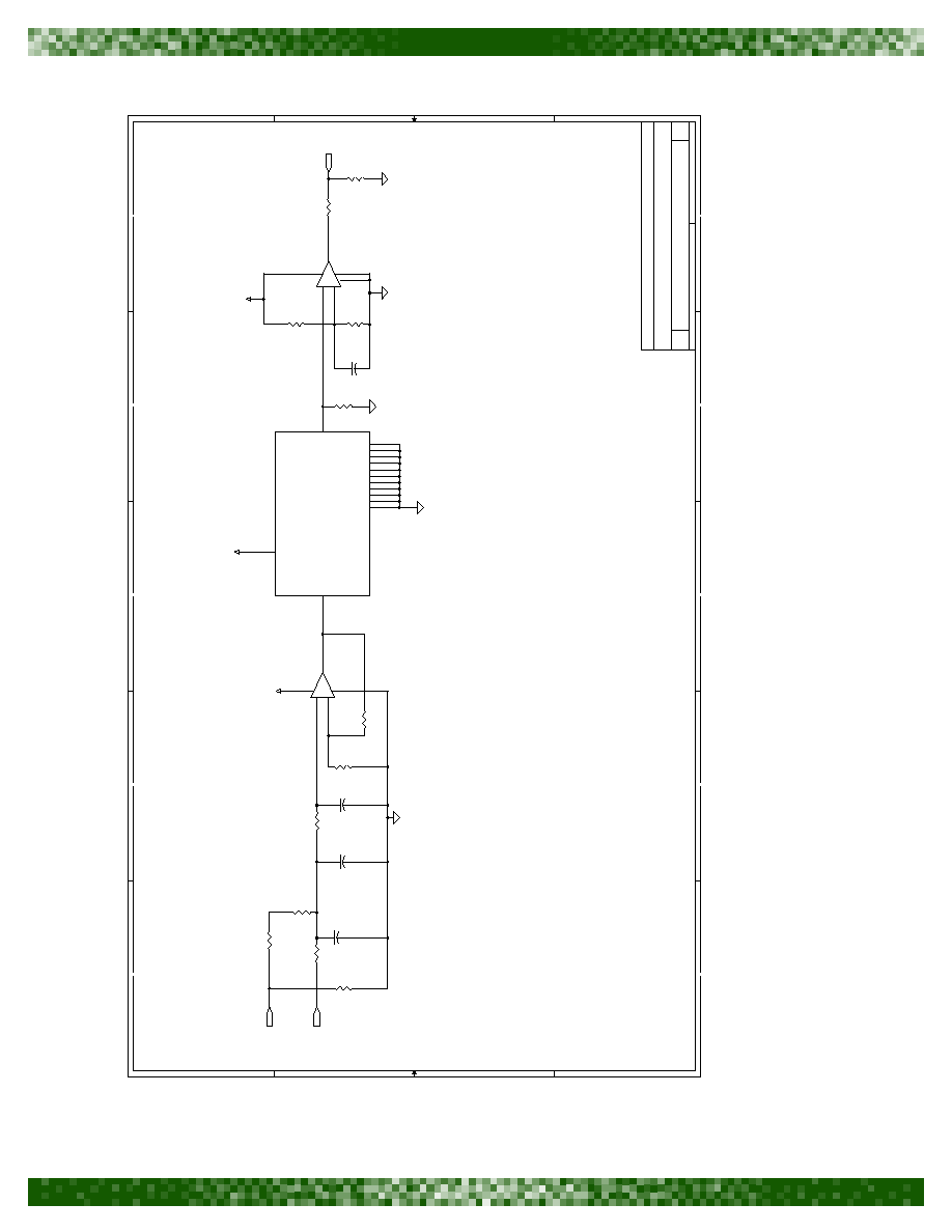
comtech aha corporation
Page 36 of 37
A subsidiary of Comtech Telecommunications Corporation
PS4540evb_0405
5
5
4
4
3
3
2
2
1
1
D
D
C
C
B
B
A
A
AGND
AGND
VCO2
DECODER
Put near receiver.
(
U
1
3
)
GND_SIGNA
L
GND_SIGNA
L
<Doc>
A
VC02, Voltage Controlled Oscillator Ckt 2
B
19
19
Friday, March 29, 2002
Ti
t
l
e
S
i
z
e
Document Number
Rev
Date:
Sheet
of
ANALO
G
_
1
6
VDD_3_3
ANALOG
_
1
2
R19
10
K
R83
51
U7
JTOS_2
0
0
Package = BK377
13
5
2
1
3
4
6
7
8
9
10
11
12
14
RF_OUT
V_TUNE
VCC_1
2V
GND
GND
GND
GND
GND
GND
GND
GND
GND
GND
GND
+
-
U17A
OP28
3
Package = SO_8
3
2
1
8
4
C6
0.033uF
R20
390
R24
3.9K
R22
1K
C7
0.033uF
R21
1M
R57
70
+
-
U8
MA
X
9
9
7
Package =
u
M
A
X
3
2
4
6
7
8
R17
3.3K
R23
1K
C8
0.033uF
R81
51
C5
0.33uF
R16
24.9K
R18
180
CLKADJ[1]
CLKADJ[0]
VCO
_
O
U
T
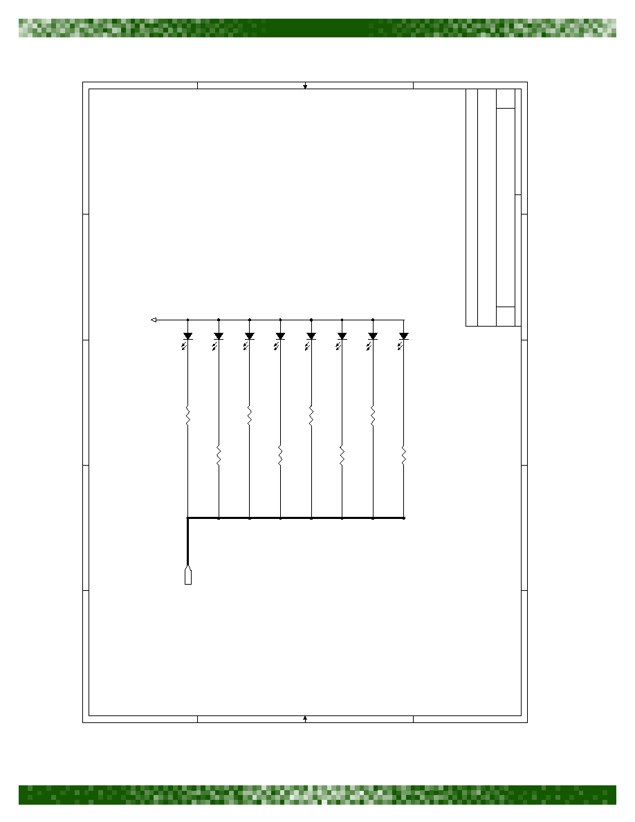
comtech aha corporation
PS4540evb_0405
A subsidiary of Comtech Telecommunications Corporation
Page 37 of 37
5
5
4
4
3
3
2
2
1
1
D
D
C
C
B
B
A
A
LEDS
AHA4540_EVB
A
LEDs
A
19
19
Friday, March 29, 2002
Title
Siz
e
Document Number
Rev
Date:
Sheet
of
LEDN0
LEDN1
LEDN2
LEDN3
LEDN6
LEDN7
LEDN5
LEDN4
LEDN[7:0]
VDD_3_3
D1
LED
Package = SS
D2
LED
Package = SS
R29
180
R28
180
D3
LED
Package = SS
D4
LED
Package = SS
R31
180
R30
180
R33
180
R32
180
R34
180
D5
LED
Package = SS
D8
LED
Package = SS
R35
180
D7
LED
Package = SS
D6
LED
Package = SS
LEDN[7:0]