AIC1084
5A Low Dropout Positive Regulator
Analog Integrations Corporation
4F, 9 Industry E. 9th Rd, Science-Based Industrial Park, Hsinchu, Taiwan
DS-1084-04 012502
TEL: 886-3-5772500
FAX: 886-3-5772510
www.analog.com.tw
1
n
FEATURES
l
Dropout Voltage 1.3V at 5A Output Current.
l
Fast Transient Response.
l
Extremely Tight Line and Load Regulation.
l
Current Limiting and Thermal Protection.
l
Adjustable Output Voltage or Fixed 1.5V, 1.8V,
2.5V, 3.3V.
l
Standard 3-Pin Power Packa
ges.
n
APPLICATIONS
l
Mother Board I/O Power Supplies.
l
Microprocessor Power Supplies.
l
High Current Regulator.
l
Post Regulator for Switching Supply.
n
DESCRIPTION
The AIC1084 is a low dropout three terminal
regulator with 5A output current capability. The
output voltage is adjustable with the use of a
resistor divider or fixed 1.5V, 1.8V, 2.5V and 3.3V.
Dropout voltage is guaranteed to be at maximum of
1.4V with the maximum output current. Its low
dropout voltage and fast transient response make it
ideal for low voltage microprocessor applications.
Current limit and thermal protection provide
protection against any overload condition that
would create excessive junction temperatures.
n
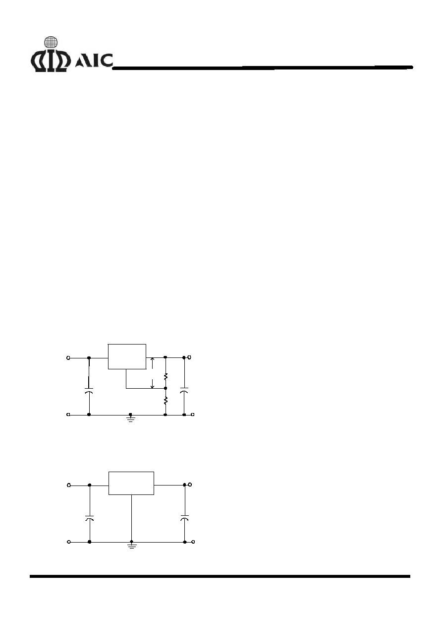
TYPICAL APPLICATION CIRCUIT
C2
10
µ
F
V
OUT
3.3V
V
IN
5V
+
+
V
REF
RF2
205
1%
ADJ
AIC1084
C1
10
µ
F
2
3
1
RF1
125
1%
V
REF
=V
OUT
-V
ADJ
=1.25V (typ.)
V
OUT
=V
REF
x (1+RF2/RF1)+ I
ADJ
x RF2
I
ADJ
=55
µ
A (typ.)
(1) C1 needed if device is far away from
filter capacitors.
(2) C2 required for stability.
Adjustable Voltage Regulator
C2
10
µ
F
V
OUT
3.3V
V
IN
5V
+
+
GND
C1
10
µ
F
AIC1084-33
2
1
3
Fixed Voltage Regulator
AIC1084
2
n
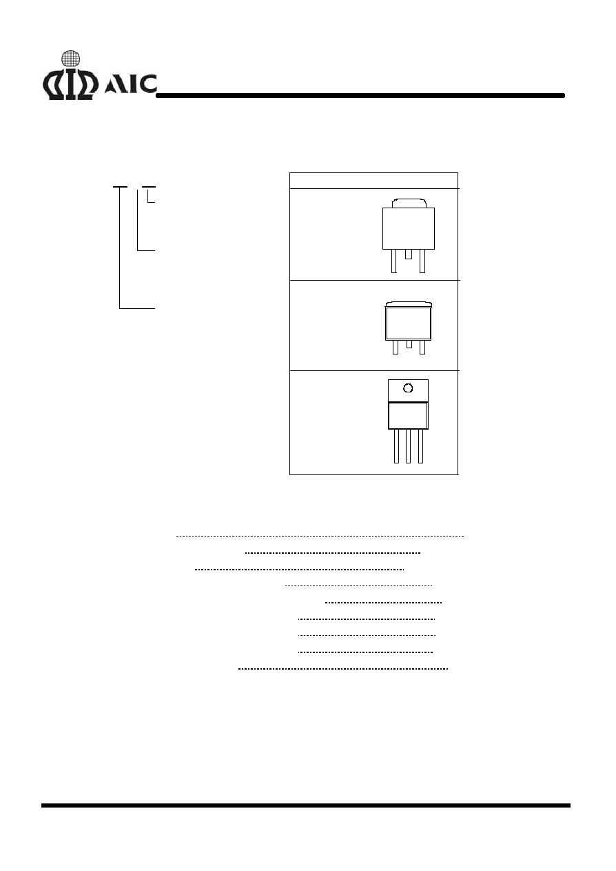
ORDERING INFORMATION
AIC1084-XXCXXX
Example: AIC1084-15CETR
ý
1.5V version in TO-252 Package
& Taping & Reel Packing Type
PIN CONFIGURATION
2
3
1
TO-252
TOP VIEW
1: ADJ (GND)
2: VOUT (TAB)
3: VIN
2
3
1
1 2
3
TO-263
TOP VIEW
1: ADJ (GND)
2: VOUT (TAB)
3: VIN
TO-220
FRONT VIEW
1: ADJ (GND)
2: VOUT (TAB)
3: VIN
PACKING TYPE
TB: TUBE
TR: TAPING & REEL
PACKAGING TYPE
E: TO-252
M: TO-263
T: TO-220
OUTPUT VOLTAGE
DEFAULT: ADJUSTABLE
15: 1.5V
18: 1.8V
25: 2.5V
33: 3.3V
n
ABSOLUTE MAXIMUM RATINGS
VIN pin to ADJ/GND pin 7V
Operating Junction Temperature Range 0
∞
C~ 125
∞
C
Storage Temperature Range - 65
∞
C ~ 150
∞
C
Thermal Resistance Junction to Case TO-252 12.5
∞
C/W
TO-263, TO-220 3
∞
C /W
Thermal Resistance Junction to Ambient TO-252 100
∞
C/W
(Assume no ambient airflow, no heatsink) TO-263 60
∞
C /W
TO-220 50
∞
C /W
Lead Temperature (Soldering) 10 sec. 260
∞
C
AIC1084
3
n
TEST CIRCUIT
Refer to TYPICAL APPLICATION CIRCUIT.
n
ELECTRICAL CHARACTERISTICS
(V
IN
=5V, T
J
=25
∞
C, I
O
=10mA, Unless otherwise
specified)
PARAMETER
TEST CONDITIONS
MIN.
TYP.
MAX.
UNIT
Reference Voltage
AIC1084 (ADJ)
T
J
=25
∞
C
1.238
1.25
1.262
V
Output Voltage
AIC1084-15, V
IN
=5V
AIC1084-18, V
IN
=5V
AIC1084-25, V
IN
=5V
AIC1084-33, V
IN
=5V
1.48
1.78
2.47
3.26
1.50
1.80
2.50
3.30
1.52
1.82
2.53
3.34
V
ADJ : 2.65V
V
IN
7V
V
OUT
=1.25V
Line Regulation
Fix : V
OUT
+1.4V
V
IN
7V
T
J
=25
∞
C
0.015
0.2
%
Load Regulation
10mA < I
O
< 5A
T
J
=25
∞
C
0.6
%
Dropout Voltage
V
OUT
,
V
REF
=1%
10mA
I
O
5A
0
∞
C
T
J
125
∞
C
1.3
1.4
V
Current Limit
0
∞
C
T
J
125
∞
C
5
6
A
Adjusted Pin Current
2.65V
V
IN
7V
55
120
µ
A
Adjusted Pin Current Change
(
I
ADJ
)
2.65V
V
IN
7V
0
∞
C
T
J
125
∞
C
0.2
5
µ
A
Temperature Stability
I
O
=0.5A
0
∞
C
T
J
125
∞
C
0.5
%
Minimum Load Current
0
∞
C
T
J
125
∞
C
5
10
mA
RMS Output Noise (% of V
OUT
)
10Hz
f
10KHz
0.003
%
Ripple Rejection Ratio
120Hz input ripple
C
OUT
=25
µ
F
(V
IN
-V
OUT
)=3V
60
72
dB
AIC1084
4
n
BLOCK DIAGRAM
VIN
55
µ
A
ADJ
V
REF
1.25V
-
+
GM
+
Thermal
Limit
Current Amp.
VOUT
GND
For fixed voltage
device
Current
Limit
n
PIN DESCRIPTIONS
ADJ PIN
-
Providing V
REF
=1.25V (typ.) for adjustable V
OUT
. V
REF
=V
OUT
-V
ADJ
and I
ADJ
=55
µ
A (typ.)
GND PIN- Power ground.
VOUT PIN -
Adjustable output voltage.
VIN PIN
-
Power Input.
n
TYPICAL PERFORMANCE CHARACTERISTICS
Fig. 1 Load Transient Response
Time (
µ
S)
Output Voltage
(V, AC)
Load Current
0
20
40
60
80
100
0.1A
2.5A
-0.4
-0.2
0
0.2
0.4
V
IN
=5.0V
C
IN
=1
µ
F(Tantalum)
C
OUT
=10
µ
F(Tantalum)
V
OUT
=3.3V
Fig. 2 Line Transient Response
Time (
µ
S)
Output Voltage
(mV, AC)
Input Voltage (V)
0
40
80
120
160
200
6.0
7.0
-100
-50
0
50
C
IN
=1
µ
F (Tantalum)
C
OUT
=10
µ
F (Tantalum)
V
OUT
=3.3V
AIC1084
5
n
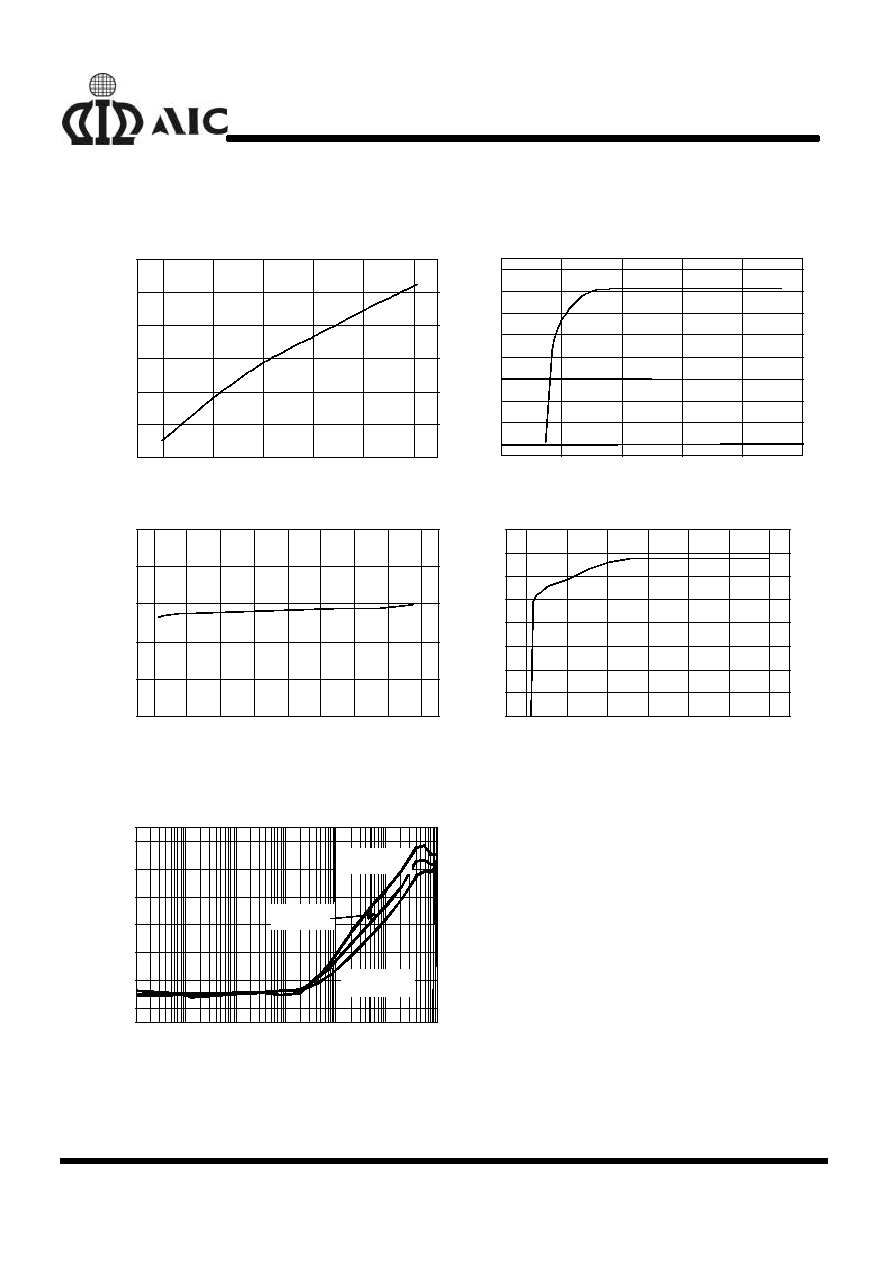
TYPICAL PERFORMANCE CHARACTERISTICS
(Continued)
Fig. 3 Dropout Voltage (V
OUT
=3.3V)
Output Current (A)
Minimum differential Voltage (V)
0
1
2
3
4
5
1.05
1.10
1.15
1.20
1.25
1.30
1.35
Fig. 4 Minimum Operating Current
Differential Voltage (V)
Minimum Operating Current (mA)
0
1
2
3
4
5
0.2
0.4
0.6
0.8
1.0
1.2
1.4
1.6
1.8
1
2
3
4
5
6
7
8
9
0
1
2
3
4
5
Fig. 5 Minimum Operating Current
Minimum
Operating Current (
mA)
Differential Voltage (V)
1
2
3
4
5
6
7
0
1
2
3
4
5
6
7
8
Fig. 6 AIC1084 (ADJ.) Short Circuit Current
Short
Circuit
Current (A)
V
IN
-V
OUT
(V)
10
1
10
2
10
3
10
4
10
5
10
6
10
7
-80
-70
-60
-50
-40
-30
-20
Fig. 7 AIC1084 (ADJ.) Ripple Rejection
C
OUT
=3.3
µ
F
Ripple Rejection Ratio (dB)
Frequency (Hz)
C
OUT
=10
µ
F
C
OUT
=25
µ
F