
AIC1340
High Performance, Tripple-Ouput, Auto-
Tracking Combo Controller
Analog Integrations Corporation
4F, 9, Industry E. 9th Rd, Science Based Industrial Park, Hsinchu Taiwan, ROC
www.analog.com.tw
DS-1340-00 May 24, 01
TEL: 886-3-5772500 FAX: 886-3-5772510
1
n
FEATURES
l
Provide Triple Accurate Regulated Voltages
l
Optimized Voltage-Mode PWM Control
l
Dual N-Channel MOSFET Synchronous Drivers
l
Fast Transient Response
l
Adjustable Over Current Protection using R
DS(on)
.
No External Current Sense Resistor Required.
l
Programmable Softstart Function
l
200KHz Free-Running Oscillator
l
Robust Outputs Auto-Tracking Characteristics
l
Sink and Source Capabilities with External Circuit
n
APPLICATIONS
l
Advanced PC Mboards
l
Information PCs
l
Servers and Workstations
l
Internet Appliances
l
PC Add-On Cards
l
DDR Termination.
n
GENERAL DESCRIPTION
The AIC1340 combines a synchronous voltage mode
PWM controller with a low dropout linear regulator
and a linear controller as well as the monitoring and
protection functions in this chip. The PWM control-
ler regulates the output voltage with a synchronous
rectified step-down converter. The built-in N-Channel
MOSFET drivers also help to simplify the design of
step-down converter. It is able to power CPUs,
GPUs, memories, and chipsets. The PWM control-
ler features over current protection using R
DS(on)
. It
improves efficiency and saves cost, as there is no
expensive current sense resistor required.
The built-in adjustable linear controller drives an ex-
ternal MOSFET to form a linear regulator that regu-
lates power for system I/O. The built-in adjustable
low dropout linear regulator can supply current up to
500mA for supplying another system I/O. Output
voltage of both linear regulators can also be adjust-
ed by means of the external resistor divider. Both
linear regulators feature current limit. With higher
load current required from the low dropout linear
regulator, the AIC1341 is recommended.
The Shutdown function is also provided for disable
the combo controller.

AIC1340
2
n
TYPICAL APPLICATION CIRCUIT
+
+
+
UGATE
PHASE
VIN2
LGATE
GATE3
PGND
FB3
VOUT2
FB2
COMP1
SS
GND
+5VIN
VCC
+12VIN
15
OCSET
4
7
11
8
6
2.5V
1.5V
VOUT2
VOUT3
+3.3VIN
12
13
16
1
2
14
14
VOUT1
+
5
GND
FB1
3
SD
10
Typical Triple-Output Application
n
ORDERING INFORMATION
ORDER NUMBER
PIN CONFIGURATION
AIC1340-XX
AIC1340CS
(SO16)
1
3
4
2
5
7
6
8
FB2
UGATE
SD
VCC
PHASE
SS
VIN2
VOUT2
OCSET
LGATE
PGND
FB3
FB1
COMP1
GATE3
G N D
16
14
15
13
12
11
9
10
PACKAGING TYPE
S: SMALL OUTLINE
TEMPERATURE RANGE
C: 0
�
C~+70
�
C

AIC1340
3
n
ABSOLUTE MAXIMUM RATING
Absolute Maximum Ratings
Supply Voltage (VCC).....................................................................................................15V
UGATE.........................................................................................GND - 0.3V to VCC + 0.3V
LGATE .........................................................................................GND - 0.3V to VCC + 0.3V
Input Output and I/O Voltage ....................................................................... GND - 0.3V to 7V
Operating Conditions
Ambient Temperature Range ...............................................................................0
�
C to 85
�
C
Maximum Operating Junction Temperature ....................................................................100
�
C
Supply Voltage, VCC..............................................................................................15V
�
10%
Thermal Information
Thermal Resistance
JA (
�
C/W)
SOIC Package ..............................................................................................100
�
C/W
Maximum Junction Temperature (Plastic Package).........................................................150
�
C
Maximum Storage Temperature Range............................................................. -65
�
C to 150
�
C
Maximum Lead Temperature (Soldering 10s)..................................................................300
�
C
n
TEST CIRCUIT
Refer to APPLICATION CIRCUIT.
AIC1340
4
n
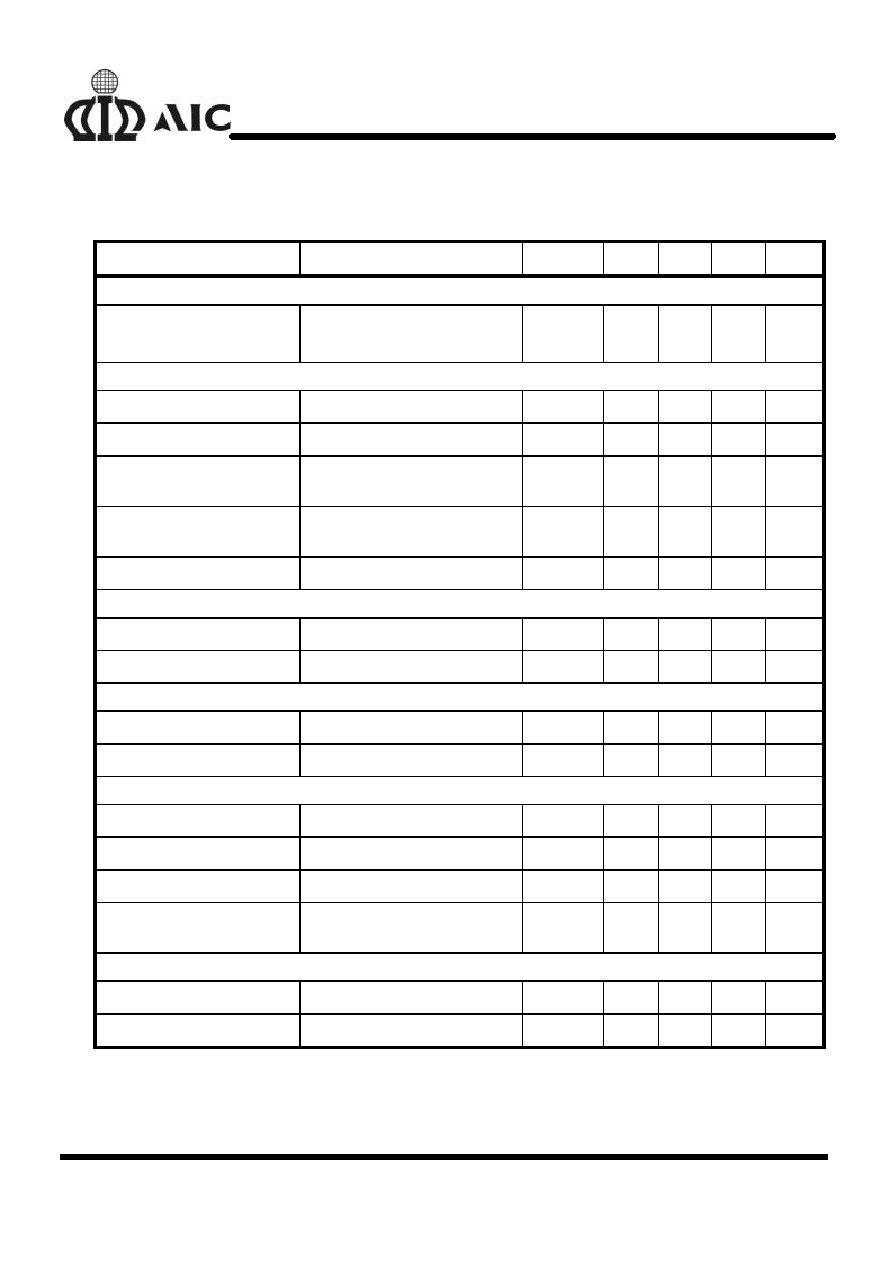
ELECTRICAL CHARACTERISTICS
(V
cc
=12V, T
J
=25
�
C, Unless otherwise
specified)
PARAMETER
TEST CONDITIONS
SYMBOL
MIN.
TYP.
MAX.
UNIT
VCC SUPPLY CURRENT
Supply Current
UGATE, LGATE, GATE3 and
VOUT2 open
I
CC
1.8
3
mA
POWER ON RESET
Rising VCC Threshold
V
OCSET
=4.5V
VCC
THR
8.6
9.5
10.4
V
Falling VCC Threshold
V
OCSET
=4.5V
VCC
THF
8.2
9.2
10.2
V
Rising VIN2 Under-Voltage
Threshold
VIN2
THR
2.5
2.6
2.7
V
VIN2 Under-Voltage Hystere-
sis
VIN2
HYS
130
mV
Rising V
OCSET1
Threshold
V
OCSETH
1.3
V
OSCILLATOR
Free Running Frequency
F
170
200
230
KHz
Ramp. Amplitude
V
OSC
1.3
V
P-P
REFERENCE
FB2 Reference Voltage
V
REF2
1.240
1.265
1.290
V
FB3 Reference Voltage
V
REF3
1.250
1.275
1.300
V
LINEAR REGULATOR
Regulation
10mA<I
OUT2
<150mA
-1
+1
%
Under-Voltage Level
FB2 falling
FB2
UV
70
82
%
Over-Current Protection
430
570
mA
Over-Current Protection
During Start-up
750
mA
LINEAR CONTROLLER
Regulation
0 < I
GATE3
< 10mA
-2.5
+2.5
%
Under-Voltage Level
FB3 falling
FB3
UV
70
80
%

AIC1340
5
n
ELECTRICAL CHARACTERISTICS
(Continued)
PARAMETER
TEST CONDITIONS
SYMBOL
MIN.
TYP.
MAX.
UNIT
PWM CONTROLLER ERROR AMPLIFIER
DC GAIN
76
dB
Gain Bandwidth Product
GBWP
11
MHz
Slew Rate
COMP1=10pF
SR
6
V/
�
S
PWM CONTROLLER GATE DRIVER
Upper Drive Source
VCC=12V, V
UGATE
=11V
R
UGH
5.2
6.5
Upper Drive Sink
VCC=12V, V
UGATE
=1V
R
UGL
3.3
5
Lower Drive Source
VCC=12V, V
LGATE
=11V
R
LGH
4.1
6
Lower Drive Sink
VCC=12V, V
LGATE
=1V
R
LGL
3
5
PROTECTION
OCSET Current Source
V
OCSET
=4.5V
DC
I
OCSET
170
200
230
�
A
Soft-Start Current
I
SS
11
�
A
Chip Shutdown Soft Start
Threshold
1.0
V
n
PIN DESCRIPTIONS
Pin 1: PHASE: Over-current detection pin. Con-
nect the PHASE pin to source of
the external high-side N-
MOSFET. This pin detects the
voltage drop across the high-side
N-MOSFET RDS(ON) for over-
current protection.
Pin 2:
UGATE: External high-side N-MOSFET
gate drive pin. Connect UGATE
to gate of the external high-side
N-MOSFET.
Pin 3:
SD:
To shut down the system, active
high or floating.
Pin 4:
VCC:
The chip power supply pin. It also
provides the gate bias charge for
all the MOSFETs controlled by
the IC. Recommended supply
voltage is 12V.
Pin 5:
SS:
Soft-start pin. Connect a capaci-
tor from this pin to ground. This
capacitor, along with an internal
10
�
A (typically) current source,
sets the soft-start interval of the
converter.
Pulling this pin low will shut down
the IC.
Pin 6:
FB2:
Connect this pin to a resistor di-
vider to set the linear regulator
output voltage.

AIC1340
6
Pin 7: VIN2:
This pin supplies power to the in-
ternal regulator. Connect this pin
to a suitable 3.3V source.
Additionally, this pin is used to
monitor the 3.3V supply. If, fol-
lowing a start-up cycle, the volt-
age drops below 2.6V (typically),
the chip shuts down. A new soft-
start cycle is initiated upon return
of the 3.3V supply above the un-
der-voltage threshold.
Pin 8:
VOUT2: Output of the linear regulator.
Supplies current up to 500mA.
Pin 9:
GND:
Signal GND for IC. All voltage
levels are measured with respect
to this pin.
Pin 10: GATE3: Linear Controller output drive pin.
This pin can drive either a Dar-
lington NPN transistor or a N-
channel MOSFET.
Pin 11: FB3
Negative feedback pin for the
linear controller error amplifier
connect this pin to a resistor di-
vider to set the linear controller
output voltage.
Pin 12: COMP1 External compensation pin. This
pin is connected to error amplifier
output and PWM comparator. An
RC network is connected to FB1
in to compensate the voltage
control feedback loop of the con-
verter.
Pin 13: FB1
The error amplifier inverting input
pin. the FB1 pin and COMP1 pin
are used to compensate the volt-
age-control feedback loop.
Pin 14: OCSET: Current limit sense pin. Connect
a resistor R
OCSET
from this pin to
the drain of the external high-side
N-MOSFET. R
OCSET
, an internal
200
�
A current source (I
OCSET
),
and the upper N-MOSFET on-
resistance (R
DS(ON)
) set the over-
current trip point according to the
following equation:
I
I
R
R
PEAK
OCSET
OCSET
DS(ON)
=
�
Pin 15: PGND:
Driver power GND pin. PGND
should be connected to a low im-
pedance ground plane in close to
lower N-MOSFET source.
Pin 16: LGATE: Lower N-MOSFET gate drive pin.

AIC1340
7
n
PACKAGE DIMENSIONS
l
16 LEAD PLASTIC SO (300 mil) (unit: mm)
SYMBOL
MIN
MAX
A
2.35
2.65
A1
0.10
0.30
B
0.33
0.51
C
0.23
0.32
D
10.10
10.50
E
7.40
7.60
e
1.27(TYP)
H
10.00
10.65
H
E
e
B
c
A
A1
D
L
L
0.40
1.27