 | –≠–ª–µ–∫—Ç—Ä–æ–Ω–Ω—ã–π –∫–æ–º–ø–æ–Ω–µ–Ω—Ç: AIC1341 | –°–∫–∞—á–∞—Ç—å:  PDF PDF  ZIP ZIP |

AIC1341
High Performance, Triple-Output, Auto-
Tracking Combo Controller
Analog Integrations Corporation 4F, 9, Industry E. 9th Rd, Science Based Industrial Park, Hsinchu Taiwan, ROC
www.analog.com.tw
DS-1341-00 May 24, 01
TEL: 886-3-5772500 FAX: 886-3-5772510
1
n
FEATURES
l
Provide Triple Accurate Regulated Voltages
l
Optimized Voltage-Mode PWM Control
l
Dual N-Channel MOSFET Synchronous Drivers
l
Fast Transient Response
l
Adjustable Over Current Protection using R
DS(ON)
.
No External Current Sense Resistor Required.
l
Programmable Softstart Function
l
200KHz Free-Running Oscillator
l
Robust Outputs Auto-Tracking Characteristics
l
Sink and Source Capabilities with External Circuit
n
APPLICATIONS
l
Advanced PC Mboards
l
Information PCs
l
Servers and Workstations
l
Internet Appliances
l
PC Add-On Cards
l
DDR Termination
n
GENERAL DESCRIPTION
The AIC1341 combines a synchronous voltage
mode PWM controller with two linear controllers
as well as the monitoring and protection functions
in this chip. The PWM controller regulates the
output voltage with a synchronous rectified step-
down converter. The built-in N-Channel MOSFET
drivers also help to simplify the design of step-
down converter. It is able to power CPUs, GPUs,
memories, chipsets and multi-voltage applications.
The PWM controller features over current protec-
tion using R
DS(ON)
. It improves efficiency and saves
cost, as there is no expensive current sense resis-
tor required.
Two built-in adjustable linear controllers drive an
external MOSFETs to form two linear regulators
that regulates power for multiple system I/O. Out-
put voltage of both linear regulators can also be
adjusted by means of the external resistor divider.
Both linear regulators feature current limit. For a
system I/O requires current less than 500mA, the
AIC1340 is recommended for saving one external
MOSFET.
The programmable soft-start design provodes a
controlled output voltage rise, which limits the cur-
rent rate during power on time.
The shutdown function is also provided for dis-
abling the combo controller.
AIC1341
2
n
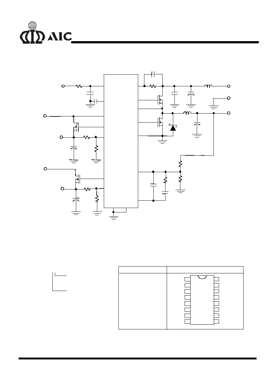
TYPICAL APPLICATION CIRCUIT
+
+
UGATE
PHASE
VIN2
LGATE
GATE3
PGND
FB3
GATE2
FB2
COMP1
SS
GND
+5VIN
VCC
+12VIN
15
OCSET
4
7
11
8
6
VOUT2
VOUT3
+3.3VIN
12
13
16
1
2
14
14
VOUT1
+
5
GND
FB1
3
SD
10
+
+3.3VIN
AIC1341CS
Q1
Q2
Typical Triple-Output Application
n
ORDERING
INFORMATION
ORDER NUMBER
PIN CONFIGURATION
AIC1341-XX
AIC1341CS
(SO 16)
PACKAGING TYPE
S: SMALL OUTLINE
TEMPERATURE RANGE
C: O
∞
C~+70
∞
C
1
3
4
2
5
7
6
8
FB2
UGATE
SD
VCC
PHASE
SS
VIN2
GATE2
OCSET
LGATE
PGND
FB3
FB1
COMP1
GATE3
G N D
16
14
15
13
12
11
9
10
AIC1341
3
n
ABSOLUTE MAXIMUM RATING
Absolute Maximum Ratings
Supply Voltage (VCC).............................................................................................................. 15V
UGATE....................................................................................................GND - 0.3V to V
CC
+ 0.3V
LGATE ....................................................................................................GND - 0.3V to V
CC
+ 0.3V
Input Output and I/O Voltage .................................................................................GND - 0.3V to 7V
Operating Conditions
Ambient Temperature Range ........................................................................................ 0
∞
C to 85
∞
C
Maximum Operating Junction Temperature ............................................................................. 100
∞
C
Supply Voltage, VCC....................................................................................................... 15V
±
10%
Thermal Information
Thermal Resistance
JA
(
∞
C/W)
SOIC Package ....................................................................................................... 100
∞
C/W
Maximum Junction Temperature (Plastic Package).................................................................. 150
∞
C
Maximum Storage Temperature Range.......................................................................-65
∞
C to 150
∞
C
Maximum Lead Temperature (Soldering 10s)........................................................................... 300
∞
C
n
TEST CIRCUIT
Refer to APPLICATION CIRCUIT.
n
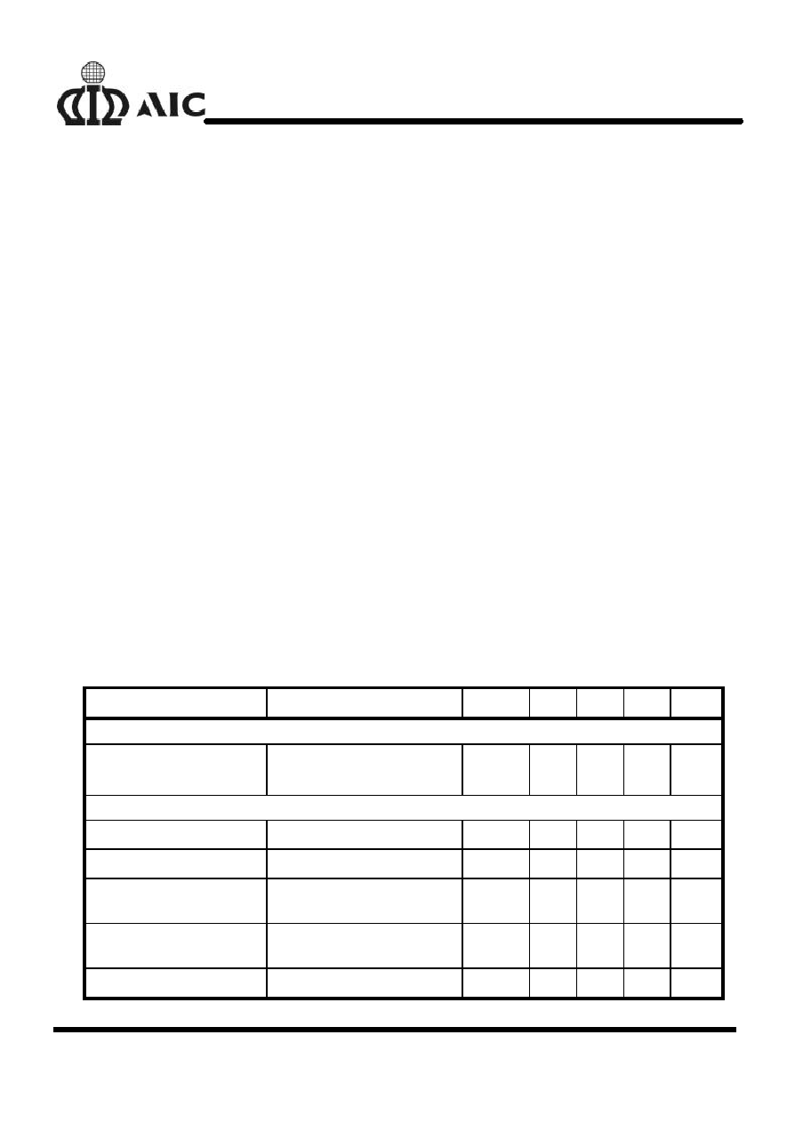
ELECTRICAL CHARACTERISTICS
(V
cc
=12V, T
J
=25
∞
C, Unless otherwise
specified)
PARAMETER
TEST CONDITIONS
SYMBOL
MIN.
TYP.
MAX.
UNIT
VCC SUPPLY CURRENT
Supply Current
UGATE, LGATE, GATE2 and
GATE3 open
I
CC
1.8
5
mA
POWER ON RESET
Rising VCC Threshold
V
OCSET
=4.5V
VCC
THR
8.6
9.5
10.4
V
Falling VCC Threshold
V
OCSET
=4.5V
VCC
THF
8.2
9.2
10.2
V
Rising VIN2 Under-Voltage
Threshold
VIN2
THR
2.5
2.6
2.7
V
VIN2 Under-Voltage Hystere-
sis
VIN2
HYS
130
mV
Rising V
OCSET1
Threshold
V
OCSETH
1.3
V
AIC1341
4
n
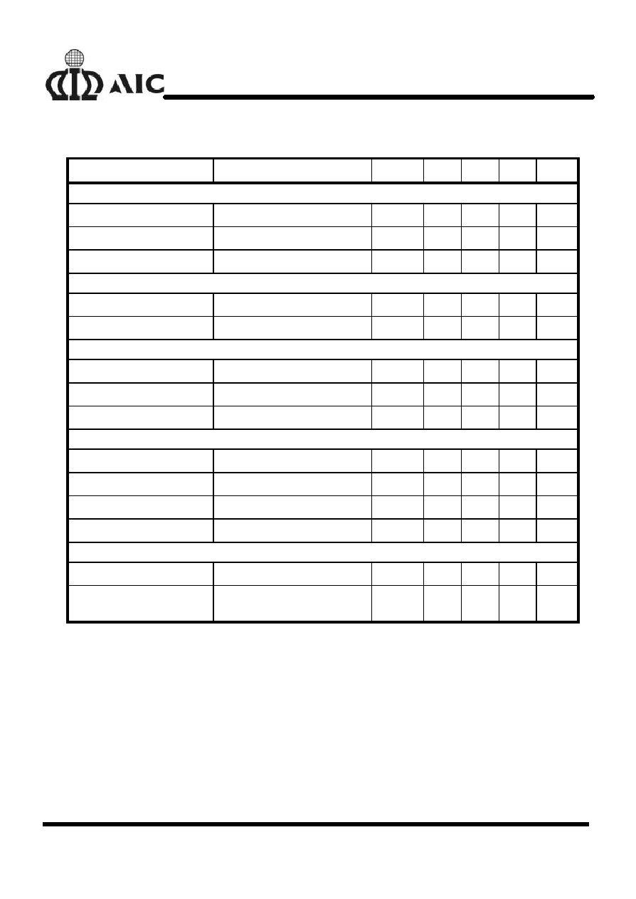
ELECTRICAL CHARACTERISTICS
(Continued)
PARAMETER
TEST CONDITIONS
SYMBOL
MIN.
TYP.
MAX.
UNIT
OSCILLATOR and REFERENCE
Free Running Frequency
F
170
200
230
KHz
FB2 Reference Voltage
V
REF2
1.245
1.270
1.295
V
FB3 Reference Voltage
V
REF3
1.250
1.275
1.300
V
LINEAR CONTROLLER
Regulation
0 < I
GATE2/3
< 10mA
-2.5
+2.5
%
Under-Voltage Level
FB2/3 falling
FB2/3
UV
70
80
%
PWM CONTROLLER ERROR AMPLIFIER
DC GAIN
76
dB
Gain Bandwidth Product
GBWP
11
MHz
Slew Rate
COMP1=10pF
SR
6
V/
µ
S
PWM CONTROLLER GATE DRIVER
Upper Drive Source
VCC=12V, V
UGATE
=11V
R
UGH
5.2
6.5
Upper Drive Sink
VCC=12V, V
UGATE
=1V
R
UGL
3.3
5
Lower Drive Source
VCC=12V, V
LGATE
=11V
R
LGH
4.1
6
Lower Drive Sink
VCC=12V, V
LGATE
=1V
R
LGL
3
5
PROTECTION
Soft-Start Current
I
SS
11
µ
A
Chip Shutdown Soft Start
Threshold
1.0
V

AIC1341
5
n
PIN DESCRIPTIONS
Pin 1: PHASE: Over-current detection pin. Con-
nect the PHASE pin to source of
the external high-side N-
MOSFET. This pin detects the
voltage drop across the high-side
N-MOSFET R
DS(ON)
for over-
current protection.
Pin 2: UGATE: External high-side N-MOSFET
gate drive pin. Connect UGATE
to gate of the external high-side
N-MOSFET.
Pin 3:
SD:
To shut down the system, active
high or floating. If connecting a
resistor to ground, keep the re-
sistor less than 4.7K
Pin 4:
VCC:
The chip power supply pin. It also
provides the gate bias charge for
all the MOSFETs controlled by
the IC. Recommended supply
voltage is 12V.
Pin 5: SS:
Soft-start pin. Connect a capaci-
tor from this pin to ground. This
capacitor, along with an internal
10
µ
A (typically) current source,
sets the soft-start interval of the
converter.
Pulling this pin low will shut down
the IC.
Pin 6:
FB2:
Connect this pin to a resistor di-
vider to set the linear regulator
output voltage.
Pin 7: VIN2:
This pin supplies power to the
internal regulator. Connect this
pin to a suitable 3.3V source.
Additionally, this pin is used to
monitor the 3.3V supply. If, fol-
lowing a start-up cycle, the volt-
age drops below 2.6V (typically),
the chip shuts down. A new soft-
start cycle is initiated upon re-
turn of the 3.3V supply above
the under-voltage threshold.
Pin 8:
GATE2: Linear Controller output drive pin.
This pin can drive either a Dar-
lington NPN transistor or a N-
channel MOSFET.
Pin 9:
GND:
Signal GND for IC. All voltage
levels are measured with respect
to this pin.
Pin 10: GATE3: Linear Controller output drive pin.
This pin can drive either a Dar-
lington NPN transistor or an N-
channel MOSFET.
Pin 11: FB3
Negative feedback pin for the
linear controller error amplifier
connect this pin to a resistor di-
vider to set the linear controller
output voltage.
Pin 12: COMP1 External compensation pin. This
pin is connected to error ampli-
fier output and PWM comparator.
A RC network is connected to
FB1 to compensate the voltage
control feedback loop of the con-
verter.
Pin 13: FB1
The error amplifier inverting input
pin. The FB1 pin and COMP1 pin
are used to compensate the volt-
age-control feedback loop.
Pin 14: OCSET: Current limit sense pin. Connect
a resistor R
OCSET
from this pin to
the drain of the external high-side
N-MOSFET. R
OCSET
, an internal
200
µ
A current source (I
OCSET
),
and the upper N-MOSFET on-
resistance (R
DS(ON)
) set the over-
current trip point according to the
following equation:
I
I
R
R
PEAK
OCSET
OCSET
DS(ON)
=
◊