AIC1401
PWM Step-Down Switching Controller with
Shutdown
Analog Integrations Corporation 4F, 9, Industry E. 9th Rd, Science Based Industrial Park, Hsinchu Taiwan, ROC
www.analog.com.tw
DS-1401-00 May 24, 01
TEL: 886-3-5772500 FAX: 886-3-5772510
1
n
FEATURES
l
Operation Voltage up to 15V
l
Voltage-Mode Operation
l
Fast Transient Response
l
Built In Accurate 1.3V Voltage Reference
l
Adjustable Over Current Protection using
R
DS(ON)
No External Current Sense Resistor
Required
l
Low Shutdown Current
l
200KHz Free-Running Oscillator
l
Built in Soft Start.
n
APPLICATIONS
l
Notebook PC
l
Advanced PC Mboards
l
Information PCs
l
Servers and Workstations
l
PC Add-On Cards
n
DESCRIPTION
The AIC1401 is a high efficiency, PWM step-
down, voltage-mode, switching controller. It is
suitable for IA, Notebook, LCD PC and LCD
monitor main power applications.
The built-in high voltage CMOS driver drives an
external N-channel MOSFET for replacing the
higher cost P-channel MOSFET in a standard
buck topology.
The 200KHz switching frequency allows using
smaller external components while maintaining
high conversion efficiency. The 11MHz
bandwidth and 6V/us slew rate of the error
amplifier ensures the higher converter
bandwidth and the fast transient response.
The AIC1401 also features over current
protection. It provides adjustable over current
trigger point and short-circuit protections by
sensing the output current across the on
resistance of the external N-channel MOSFET
rather then an expensive external low value
sense resistor.
n
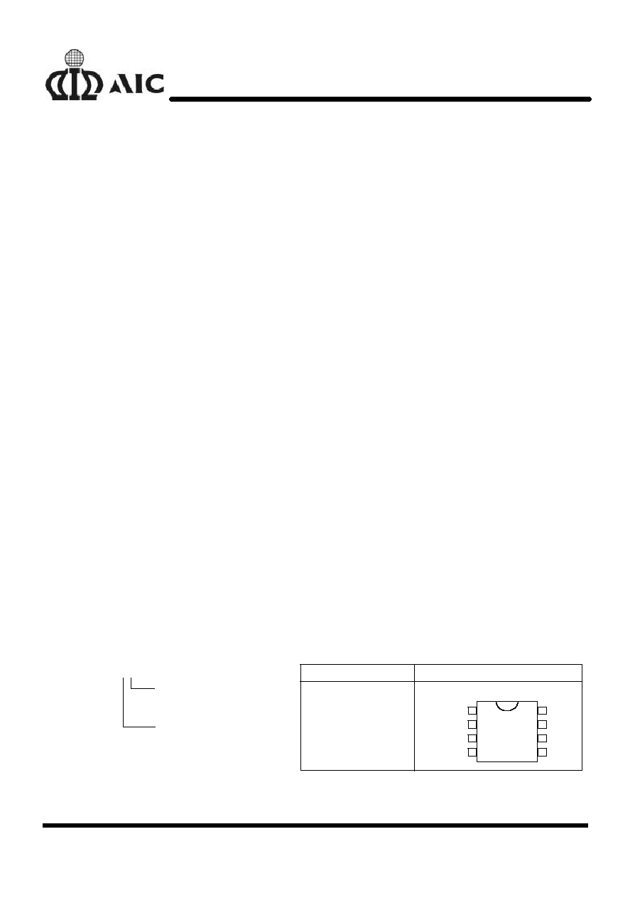
ORDERING INFORMATION
ORDER NUMBER
AIC1401CS
(SOP8)
PIN CONFIGURATION
TOP VIEW
LX
1
3
4
2
VCC
/SHDN
COMP
FB
UG
GND
8
6
5
7
OCSET
PACKAGE TYPE
S: SMALL OUTLINE
TEMPERATURE RANGE
C: 0
�
C ~+70
�
C
AIC1401-XX
AIC1401
2
n
TYPICAL APPLICATION CIRCUIT
AIC1401
*C1
1
�
F
C5
33P
C6
1000P
C2
1000P
+
C4
330
�
FX3
+
C3
470
�
F
R4
13K
R3
2K
R6
5K
R2
90.9K
R5 10
R1
2.2K
L2
7
�
H
L1
1.5
�
H
D1
SRA1620
M1
IR3303
1.5V/5A
*C1 must be very close
to VCC PIN
V
OUT
5V
12V
OCSET
/SHDN
COMP
FB
VCC
UG
LX
GND
DC/DC Converter
n
ABSOLUTE MAXIMUM RATINGS
Supply Voltage, V
CC
....... ...... ... ... ............................... ... ... ... ......................................... 15V
Input, Output, or I/O Voltage .................. ... ... ... ... ... ....... ... ......... GND - 0.3V to VCC+0.3V
ESD Classification ................................ ... ... ... ........ ... ................. ... ......................... Class 2
Recommended Operating Conditions
Supply Voltage, V
CC
....... ......................... ... ... ... .......... ... ... .................................. 12V
�
10%
Ambient Temperature Range .... ................................... ... ... ... .... ... ... .................. 0
�
C~70
�
C
Junction Temperature Range ....... ............... ... ... ............ ..... ... ......................... 0
�
C~ 100
�
C
Thermal Information
Thermal Resistance,
JA
(Typical, Note 1)
SOIC Package .................................. ... ... ... ... ... ... ... ... ..... ... ... ... ... ........... . 100
�
C/W
SOIC Package (with 3 in
2
of Copper) ... ... ... ... ... ... ... ... ... ... ... ... ... ... ......... .. 90
�
C/W
Maximum Junction Temperature (Plastic Package) ... ... ... .... ... ..... ... ... ................... 150
�
C
Maximum Storage Temperature Range ... ... ... ... ..... ... ... ... ......... ... .... ......... �65
�
C~150
�
C
Maximum Lead Temperature (Soldering 10 Sec) ... ... ... ... ... ... ... ...... ... ......... ......... 300
�
C
Note 1:
JA
is measured with the component mounted on an evaluation PC board in free air.
n
TEST CIRCUIT
Refer to TYPICAL APPLICATION CIRCUIT.
AIC1401
3
n
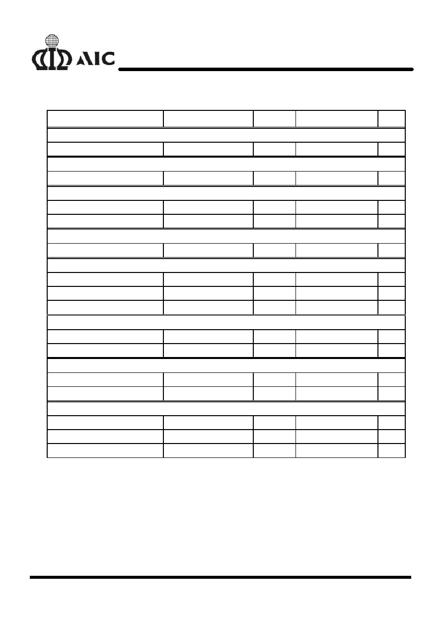
ELECTRICAL CHARACTERISTICS
(VCC= 12V, Ta=25
�
C, unless otherwise
specified.)
PARAMETER
TEST CONDITIONS
SYMBOL
MIN.
TYP.
MAX.
UNIT
VCC Supply Current
Nominal Supply
UGATE Open
I
VCC
2
mA
Power-On Reset
V
CC
Threshold
V
OCSET
=4.5V
9.5
V
Oscillator
Frequency
200
KHz
Duty Cycle
88
%
Internal Reference Voltage
Reference Voltage
1.27
1.30
1.33
V
Error Amplifier
DC Gain
76
dB
Gain-Bandwidth Product
GBW
11
MHz
Slew Rate
SR
6
V/
�
S
Gate Driver
Upper Gate Source
R
UGATE
7
Upper Gate Sink
R
UGATE
5
Protection
OCSET Current Source
V
OCSET
=4.5VDC
I
OCSET
200
�
A
SS Current
I
SS
10
�
A
Shutdown
Shutdown Low Input
V
IN
L
0.35
V
Shutdown High Input
V
IN
H
2
V
Shutdown Mode Current
1
�
A

AIC1401
4
n
PIN DESCRIPTIONS
PIN 1: OCSET- Current limit sense pin. Connect
a resistor R
OCSET
from this pin to
the drain of the external
MOSFET. R
OCSET
, an internal
200
�
A current source (I
OCSET
),
and the external MOSFET on-
resistance (R
DS(ON)
) jointly set
the
overcurrent trip point
according to the following
equation:
I
I
R
R
PEAK
OCSET
OCSET
DS(ON
=
�
)
If FB pin voltage is sensed to be
below 50% of the internal
voltage reference, the
overcurrent comparator cycles
the soft-start function.
PIN 2: /SHDN - Shutdown pin. Connect this pin
to ground for shutdown.
PIN 3: COMP - External compensation pin. This
pin is connected to error
amplifier output and PWM
comparator. A RC network is
connected to FB pin to
compensate the voltage-control
feedback loop of the converter.
PIN 4: FB - The error amplifier inverting
input pin. The FB pin and COMP
pin are used to compensate the
voltage-control feedback loop.
PIN 5: GND - Ground pin.
PIN 6: LX - Overcurrent detection pin.
Connect the LX pin to source of
the external N-MOSFET. This
pin detects the voltage drop
across the MOSFET R
DS(ON)
for
overcurrent protection.
PIN 7: UG - External MOSFET gate drive pin.
Connect this pin to gate of the
external MOSFET.
PIN 8: VCC - The chip power supply pin.
Recommended supply voltage is
12V.
n
APPLICATION CIRCUIT
Refer to TYPICAL APPLICATION CIRCUIT
AIC1401
5
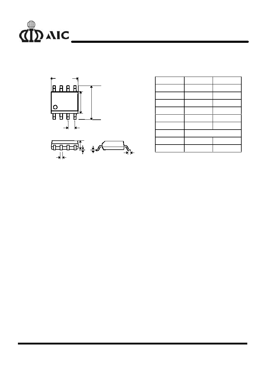
PHYSICAL DIMENSIONS
l
8 LEAD PLASTIC SO (unit: mm)
SYMBOL
MIN
MAX
A
1.35
1.75
A1
0.10
0.25
B
0.33
0.51
C
0.19
0.25
D
4.80
5.00
E
3.80
4.00
e
1.27(TYP)
H
5.80
6.20
L
0.40
1.27
D
H
e
A
B
A1
C
E
L