AIC1550
Low-Noise Synchronous PWM Step-Down
DC/DC Converter
FEATURES
95% Efficiency or up
800mA Guaranteed Output Current.
Adjustable Output Voltage from 0.75V to VIN
of a range from +2.5V to 6.5V.
Very Low Quiescent Current: 35
µA (Typ.).
Fixed- 500KHz or Adjustable Frequency
Synchronous PWM Operation.
Synchronizable external Switching
Frequency up to 1MHz.
Accurate Reference: 0.75V (±2%).
100% Duty Cycle in Dropout.
Low Profile 8-Pin MSOP Package.
APPLICATIONS
PDAs.
Digital Still Cameras.
Handy-Terminals.
Cellular Phones.
C
PU I/O Supplies.
Cordless Phones.
Notebook Chipset Supplies.
Battery-Operated Devices (4 NiMH/
NiCd
or 1
Li-ion
Cells).
DESCRIPTION
The AIC1550 is a low-noise pulse-width-
modulated (PWM) DC-DC step-down converter.
It powers logic circuits in PDAs and small
wireless systems such as cellular phones,
handy-terminals.
The device features an internal synchronous
rectifier for high conversion efficiency. Excellent
noise characteristics and fixed-frequency
operation provide easy post-filtering. The
AIC1550 is ideally suited for Li-ion battery
applications. It is also suitable for +3V or +5V
fixed input applications. The device can operate
in either one of the following four modes.
(1) Forced PWM mode operates at a
fixed frequency regardless of the
load.
(2) Synchronizable PWM mode
allows the synchronization by
using an external switching
frequency with a minimum
harmonics.
(3) PWM/PFM Mode extends battery
life by switching to a PFM pulse-
skipping mode under light loads.
(4) Shutdown mode sets device to
standby, reducing supply current
to 0.1µA or under.
The AIC1550 can deliver over 800mA output
current. The output voltage can be adjusted
from 0.75V to VIN ranging from +2.5V to +6.5V.
Other features of the AIC1550 include low
quiescent current, low dropout voltage, and a
0.75V reference of ±2% accuracy. It is available
in a space-saving 8-pin MSOP package.
Analog Integrations Corporation
Si-Soft Research Center
DS-1550P-04 010405
3A1, No.1, Li-Hsin Rd. I , Science Park , Hsinchu 300, Taiwan , R.O.C.
TEL: 886-3-5772500
FAX: 886-3-5772510
www.analog.com.tw
1
AIC1550
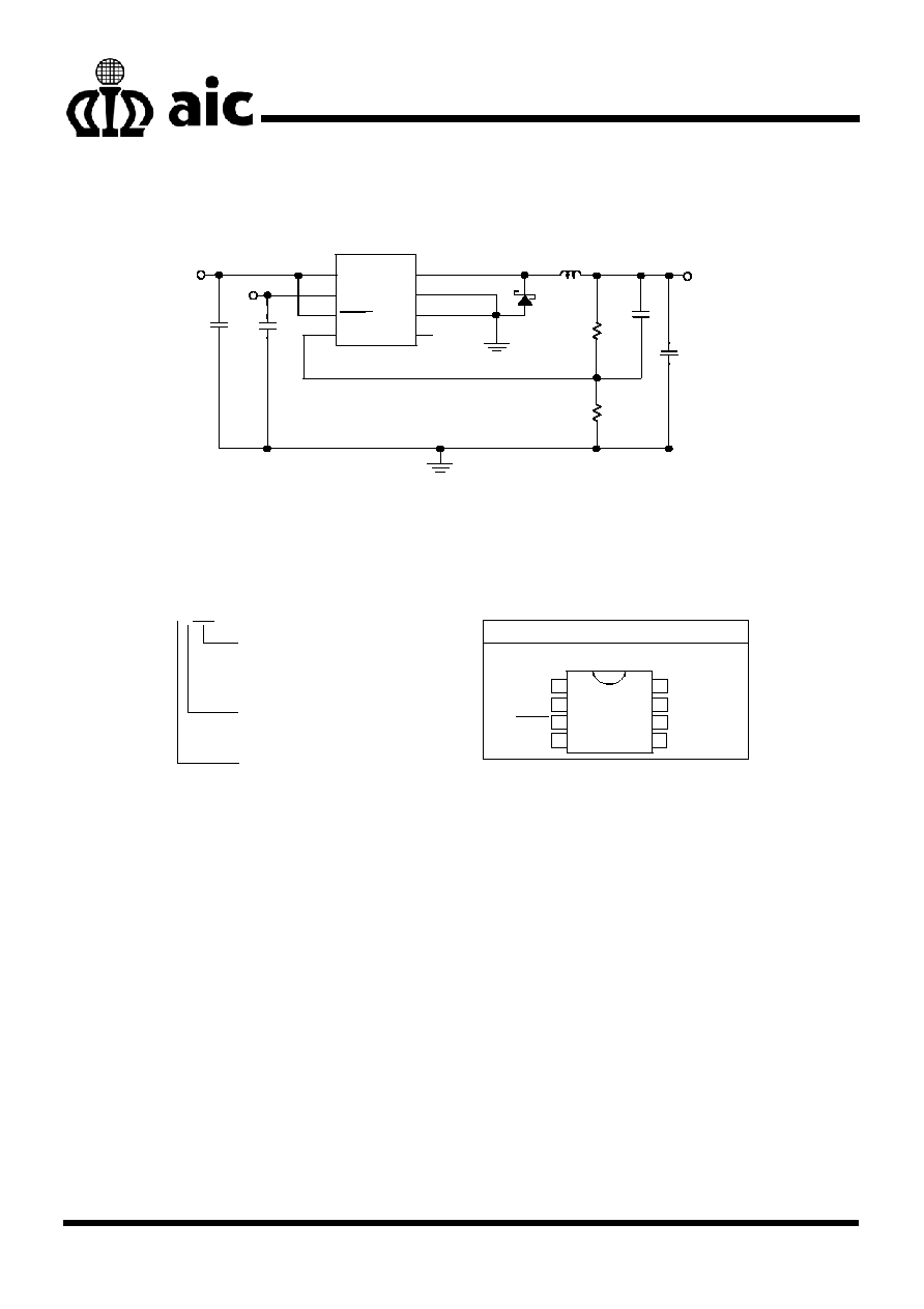
TYPICAL APPLICATION CIRCUIT
SS12
*
R2
560K
R1
820K
L1
6.8
µH
C
O
22
µF
C
IN
22
µF
CF
12P
C
BP
0.1
µF
LX
BP
SYNC/
MODE
FB
RT
Optional
V
OUT
= 1.8V
IN
= 2.5V to 6.5V
SHDN
AIC1550
GND
VIN
BP
1
2
3
4
5
6
7
8
* Note: Efficiency can boost 2% to 4% if D1 is connected.
C
IN
: TAIYO YUDEN LMK316F226ZL-T Ceramic capacitor
C
O1
: TAIYO YUDEN LMK316F226ZL-T Ceramic capacitor
L1: TDK SLF6025-6R8M1R3
D1: GS SS12
D1
V
ORDERING INFORMATION
PACKING TYPE
TR: TAPE & REEL
TB: TUBE
PACKAGING TYPE
O:MSOP8
C: Commercial Degree
P: Lead Free
PIN CONFIGURATION
TOP VIEW
AIC1550XXXX
SYNC/MODE
LX
GND
RT
SHDN
BP
FB
VIN 1
3
4
2
8
6
5
7
Example: AIC1550COTR
In MSOP Package & Taping &
Reel Packing Type
AIC1550POTR
In MSOP Lead Free Package &
Taping & Reel Packing Type
2

AIC1550
ABSOLUTE MAXIMUM RATINGS
VIN, BP, SHDN, SYNC/MODE, RT to GND
-0.3 to +7V
BP to VIN
.-0.3 to 0.3V
LX to GND
-0.3 ~ (V
IN
+0.3V)
FB to GND
-0.3 ~ (V
BP
+0.3V)
Operating Temperature Range
-40
∞C ~ 85∞C
Junction Temperatrue
125
∞C
Storage Temperature Range
- 65
∞C ~ 150∞C
Lead Temperature (Soldering. 10 sec)
260
∞C
Absolute Maximum Ratings are those values beyond which the life of a device may be
Impaired.
TEST CIRCUIT
Refer to Typical Application Circuit.
3

AIC1550
ELECTRICAL CHARACTERISTICS
(V
IN
=+3.6V, T
A
=+25
∞C, SYNC/MODE =GND,
SHDN
=IN, unless otherwise specified.) (Note1)
PARAMETER SYMBOL
CONDITIONS
MIN
TYP
MAX
UNITS
Input Voltage Range
V
IN
2.5 6.5 V
Output Adjustment Range
V
OUT
V
REF
V
IN
V
Feedback Voltage
V
FB
0.735 0.75 0.765
V
Line Regulation
Duty Cycle = 100% to 23%
+1
%
Load Regulation
I
OUT
= 0 to 800mA
-1.3
%
FB Input Current
I
FB
V
FB
= 1.4V,
-50
0.01
50
nA
V
IN
= 3.6V
0.32
0.65
P-Channel On-Resistance P
RDS(ON)
I
LX
= 100mA
V
IN
= 2.5V
0.38
V
IN
= 3.6V
0.32
0.65
N-Channel On-Resistance N
RDS(ON)
I
LX
= 100mA
V
IN
= 2.5V
0.38
P-Channel Current-Limit
Threshold
(Note
2)
1 1.5 2.1 A
Quiescent Current
SYNC/MODE = GND,
V
FB
= 1.4V, LX unconnected
35 70
µA
Shutdown Supply Current
SHDN
= LX = GND, includes LX
leakage current
0.1 1
µA
LX Leakage Current
V
IN
= 5.5V, V
LX
= 0 or 5.5V
-20
0.1
20
µA
Oscillator Frequency
f
OSC
400 500 600 KHz
SYNC Capture Range
500
1000
KHz
Maximum Duty Cycle
duty
MAX
100
%
Undervoltage Lockout
Threshold
UVLO
V
IN
rising, typical hysteresis is
85mV
1.9 2.0 2.1 V
Logic Input High
V
IH
SHDN
, SYNC/MODE, LIM
2
V
Logic Input Low
V
IL
SHDN
, SYNC/MODE, LIM
0.4
V
Logic Input Current
SHDN
, SYNC/MODE, LIM
-1
0.1
1
µA
SYNC/MODE Minimum
Pulse Width
High or low
500
nS
Note 1: Specifications are production tested at TA=25
∞C. Specifications over the -40∞C to 85∞C operating
temperature range are assured by design, characterization and correlation with Statistical
Quality Controls (SQC).
Note 2: Maximum specification is guaranteed by design, not production tested.
4

AIC1550
TYPICAL PERFORMANCE CHARACTERISTICS
(T
A
=25
o
C, V
IN
=3.6V, SYNC/MODE=GND, with Schottky diode D1, unless otherwise noted.)
Ef
ficiency (
%
)
Fig. 1 Load Current vs. Efficiency (V
OUT
=1.2V)
(Refer to typical application circuit)
Load Current (mA)
0.1
1 10
100
1000
40
50
60
70
80
90
100
V
IN
=2.1V
V
IN
=2.3V
V
IN
=5.0V
V
IN
=6.5V
V
OUT
=1.2V
E
f
fi
ci
en
cy
(
%
)
Fig. 2 Load Current vs. Efficiency (V
OUT
=1.5V)
(Refer to typical application circuit)
(R f
t t i l
li ti
i
it)
0.1
1
10
100
1000
40
50
60
70
80
90
100
Load Current (mA)
V
IN
=2.1V
V
IN
=3.3V
V
IN
=5.0V
V
IN
=6.5V
V
OUT
=1.5V
0.1
1
10
100
1000
40
50
60
70
80
90
100
Load Current (mA)
Ef
ficie
ncy
(
%
)
Fig. 3 Load Current vs. Efficiency (V
OUT
=1.8V)
(Refer to typical application circuit)
V
IN
=2.1V
V
IN
=3.3V
V
IN
=5.0V
V
IN
=6.5V
V
OUT
=1.8V
0.1
1
10
100
1000
40
50
60
70
80
90
100
Load Current (mA)
Ef
ficie
n
c
y
(%)
Fig. 4 Load Current vs. Efficiency (V
OUT
=2.5V)
(Refer to typical application circuit)
V
IN
=5.0V
V
IN
=6.5V
V
IN
=3.3V
V
OUT
=2.5V
Ef
ficien
cy (
%
)
Fig. 5 Load Current vs. Efficiency (V
OUT
=3.0V)
(Refer to typical application circuit)
0.1
1
10
100
1000
40
50
60
70
80
90
100
Load Current (mA)
V
IN
=3.6V
V
OUT
=3.0V
V
IN
=4.2V
0.1
1
10
100
1000
40
50
60
70
80
90
100
Load Current (mA)
Ef
ficien
cy (
%
)
Fig. 6 Load Current vs. Efficiency (V
OUT
=3.3V)
(Refer to typical application circuit)
V
OUT
=3.3V
V
IN
=6.5V
V
IN
=5.0V
V
IN
=4.2V
V
IN
=3.6V
5