 | ÐлекÑÑоннÑй компоненÑ: AIC1566CS | СкаÑаÑÑ:  PDF PDF  ZIP ZIP |
Äîêóìåíòàöèÿ è îïèñàíèÿ www.docs.chipfind.ru

AIC1566
4-bit DAC, Simple PWM Power Regulator With
Linear Controller
Analog Integrations Corporation
4F, 9, Industry E. 9th Rd, Science Based Industrial Park, Hsinchu Taiwan, ROC
www.analog.com.tw
DS-1566-00
TEL: 886-3-5772500
FAX: 886-3-5772510
1
FEATURES
Switching Regulator and Low Dropout Linear
Regulator on Single Chip.
Simple Voltage-Mode PWM Control.
Fast Transient Response.
±1.5% 4-Bit Digital-to-Analog Output Voltage.
Adjustable Current Limit Without External Sense
Resistors.
Full 0% to 100% Duty Ratio.
200KHz Free-Running Oscillator Programmable
up to 350KHz.
Power-Good Output Voltage Monitor.
Short Circuit Protection with Low Short Circuit
Output Current.
APPLICATIONS
Power Supply for Pentium, Pentium Pro, Power
PC, and Alpha Microprocessors.
High-Power 5V to 3.xV DC/DC Regulators.
Low-Voltage Distributed Power Supplies.
DESCRIPTION
The AIC1566 is a high power, high efficiency
switching regulator controller optimized for high
performance microprocessor applications. It is
designed to drive an N-channel MOSFET in a
standard buck topology. Featuring a low
dropout linear regulator and a digitally
programmable switching regulator, the AIC1566
includes monitoring and protection capabilities in
addition to all the essential PWM control
functions.
The internal 4-bit Digital-to-Analog Converter
(DAC) adjusts the output voltage from 2.0V to
3.5V in 0.1V increments. The precision reference
and voltage-mode control can provide output
regulation within
±1.5% over temperature and line
voltage shifts.
The internal oscillator of the AIC1566 free runs at
200KHz and can be adjusted up to 350KHz. The
resulting PWM duty ratio ranges from 0% to 100%.
The error amplifier features a 11MHz bandwidth
and 6V/
µS slew rate which enables high
converter bandwidth for fast transient
performance.
The AIC1566 provides adjustable over current
and short circuit protections. It senses the output
current across the on resistance of the N-channel
MOSFET without an external low value sense
resistor. It also monitors the output voltage with a
window comparator and issues a power good
signal when the output is within 10% of the rated
output voltage.
AIC1566
2
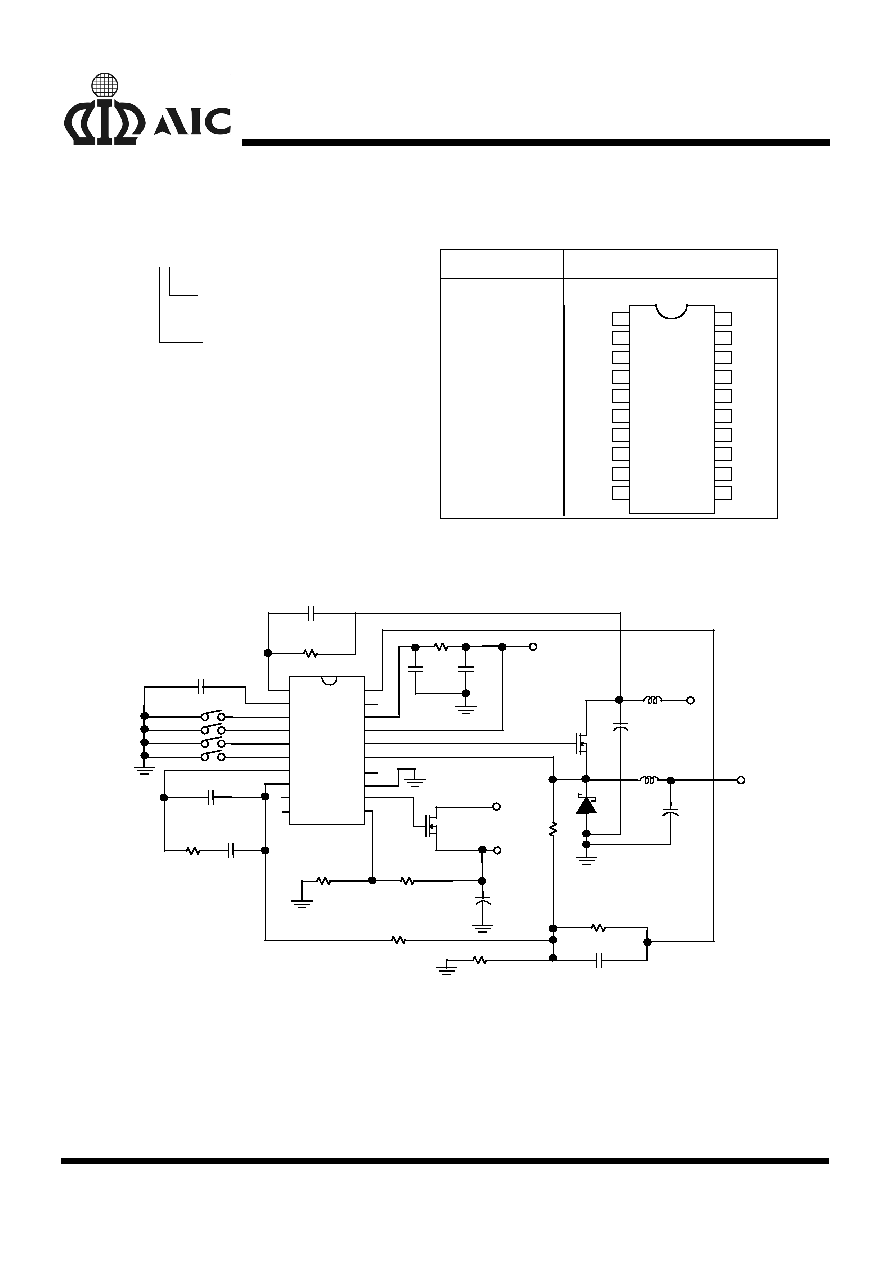
ORDERING INFORMATION
AIC1566 XX
PACKAGE TYPE
S: SMALL OUTLINE
TEMPERATURE RANGE
C: 0
°C~70°C
PIN CONFIGURATION
ORDER NUMBER
AIC1566CS
(PLASTIC SO)
TOP VIEW
VSEN
RT/OVP
VCC
BOOT
UGATE
PHASE
PGOOD
GND
LIDRI
VLFB
20
19
18
17
16
15
14
13
12
11
1
2
3
4
5
6
7
8
9
10
OCSET
SS
VID0
VID1
VID2
VID3
COMP
FB
CLP
CLN
TYPICAL APPLICATION CIRCUIT
90.9K
+
+
+
M1
OCSET
SS
VID0
VID1
VID2
VID3
COMP
FB
CLP+
CLN
VSEN
RT/OVP
VCC
BOOT
UGATE
PHASE
PGOOD
LIDRI
GND
VLFB
1000pF
R6
C6
33pF
C7
0.1
µF
C8
1000pF
C9
2.2K
R2
137
1%
R11
1.2M
3.01K
R12
R5
0.1
µF
47K
C5
R3
L1
10A
5V
V
CORE
R1 10
1
µF
12V
C1
FD3055
0.1
µF
5V
C2
R10
237
1%
V
I/O
3.3V
10A
C10
1000
µF
1
µH
RFP45N03L
C3
1000
µF x 2
7
µH
C4
1000
µF x 6
R4
15K
BYV1
1
8
D1
L2
AIC1566
Pentium
Pro V
CORE
and V
I/O
Power Supply
AIC1566
3
ABSOLUTE MAXIMUM RATINGS
Supply Voltage, V
CC
.................................................................................................... 15V
Boot Voltage, V
BOOT
................................................................................................. 15V
Input, Output or I/O Voltage ....................................................... GND -0.3V to VCC+0.3V
ESD Classification
............................................................................................. Class 2
Recommended Operating Conditions
Supply
Voltage
,
V
CC
......................................................................................... 12V
± 10%
Ambient Temperature Range .......................................................................... 0
°C ~ 70°C
Junction Temperature Range ....................................................................... 0
°C ~100°C
Thermal Information
Thermal
Resistance
,
JA
(Typical, Note 1)
SOIC Package ............................................................................................ 100
°C/W
SOIC Package (with 3 in2 of Copper) .......................................................... 90
°C/W
Maximum Junction Temperature (Plastic Package) .............................................. 150
°C
Maximum Storage Temperature Range ................................................. -65
°C~150°C
Maximum Lead Temperature (Soldering 10 sec) ............................................... 300
°C
Note 1:
JA
is measured with the component mounted on an evaluation PC board in free air.
TEST CIRCUIT
Refer to TYPICAL APPLICATION CIRCUIT.
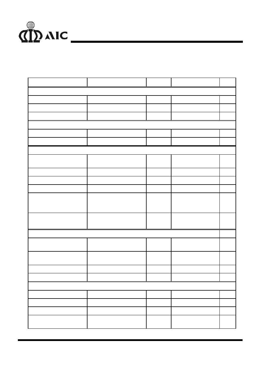
ELECTRICAL CHARACTERISTICS
(VCC= 12V, Ta=25
°
°
°
°C, unless otherwise
specified.)
PARAMETER
TEST CONDITIONS
SYMBOL
MIN.
TYP.
MAX.
UNIT
VCC Supply Current
Nominal Supply
UGATE Open
I
VCC
2
mA
Power-On Reset
V
CC
Threshold
V
OCSET
=4.5V
7
8.5
V
Rising V
OCSET
Threshold
1.26
V
Reference and DAC
DACOUT Voltage Accuracy
-1.5
+1.5
%
Oscillator
Free Running Frequency
RT Open
170
200
230
KHz
Total Variation
6K
R
T
200K
-20
+20
%
Ramp Amplitude
RT Open
V
OSC
1.5
V
P-P
AIC1566
4
ELECTRICAL CHARACTERISTICS
(Continued)
PARAMETER
TEST CONDITIONS
SYMBOL
MIN.
TYP.
MAX.
UNIT
Error Amplifier
DC Gain
76
dB
Gain-Bandwidth Product
GBW
11
MHz
Slew Rate
SR
6
V/
µS
Gate Driver
Upper Gate Source
R
UGATE
8
12
Upper Gate Sink
R
UGATE
5.5
10
Protection
Over-Voltage Trip (V
VSEN
/
V
VDAC
)
106
115
125
%
OCSET Current Source
V
OCSET
=4.5VDC
I
OCSET
170
200
230
µA
OVP Sourcing Current
V
VSEN
=5.5V, V
OVP
=0V
I
OVP
30
mA
SS Current
I
SS
10
µA
SS Sink Current under
Current Limit
V
VSEN
=VDAC, V
OCSET
=5.0V,
V
PHASE
=0V
V
FB
=VDAC-50mA
130
µA
SS Sink Current under Hard
Current Limit
V
VSEN
=0, V
OCSET
=5.0V,
V
PHASE
=0V, V
FB
=0V
65
mA
Power Good
Upper Threshold (V
VSEN
/
V
DAC
)
V
VSEN
Rising
106
114
%
Lower Threshold (V
VSEN
/
V
DAC
)
V
VSEN
Falling
84
94
%
Hysteresis (V
VSEN
/ V
DAC
)
Upper and Lower Threshold
2
%
PGOOD Voltage Low
I
PGOOD
=5mA
V
PGOOD
0.5
V
Linear Regulator
VLFB Feedback Voltage
Hysteresis (V
VSEN
/V
DAC
)
1.18
1.21
1.24
V
VLFB Bias Current
40
nA
LIDRI Sourcing Current
10
mA
CLP, CLN, Current Limiting
Threshold
10
20
30
mV
AIC1566
5
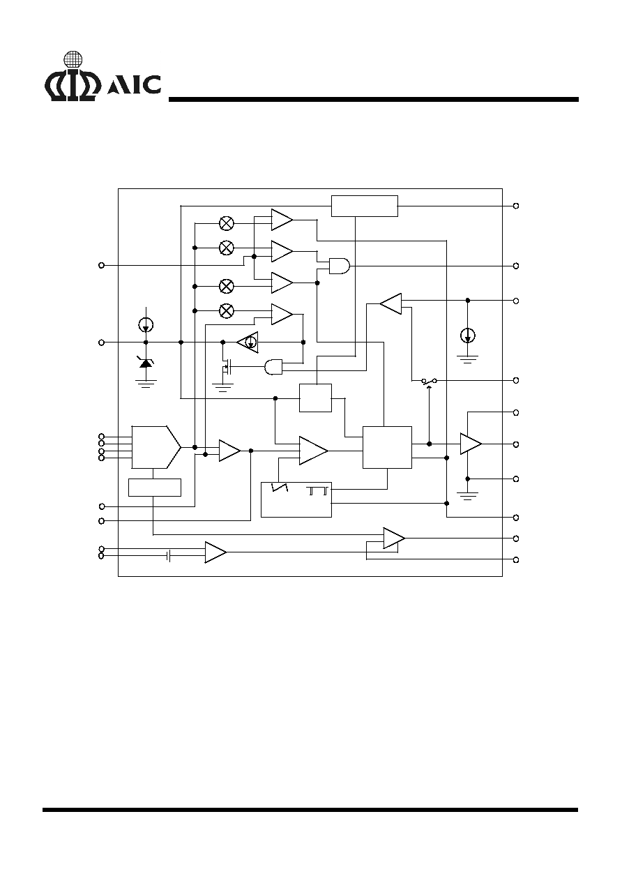
BLOCK DIAGRAM
PWM
COMPARATOR
CURRENT SENSE AMP.
LINEAR AMP.
ERROR
AMP
CLN
VDAC
1.2V
CLP
COMP
FB
VLFB
LIDRI
OSCILLATOR
REFERENCE
VID0
VID3
VID2
VID1
4BITS
DAC
RT/OVP
PHASE
GND
BOOT
UGATE
OVER
CURRENT
VSEN
OCSET
SOFT
START
10
µA
4V
200
µA
CONTROL
LOGIC
OVP
POWER-ON
RESET
VCC
50%
POWER
GOOD
SS
90%
PGOOD
110%
115%
20mV
+
-
+
-
+
-
+
-
+
+
-
+
-
+
-
+
-
+
-
+
-
AIC1566
6
PIN DESCRIPTION
PIN 1: OCSET - Current limit sense pin. Connect
a resistor R
OCSET
from this pin to
the drain of the external
MOSFET. R
OCSET
, an internal
200
µA current source (I
OCSET
),
and the external MOSFET on-
resistance (R
DS(ON)
) jointly set
the over current trip point
according to the following
equation:
I
I
R
R
PEAK
OCSET
OCSET
DS(ON
=
×
)
If FB pin voltage is sensed to
be below 50% of the internal
voltage reference VDAC, the
over current comparator
cycles the soft-start function.
PIN
2: SS
- Soft start pin. Connect a
capacitor from this pin to ground.
An internal 10
µA current source
provides soft start function for
the converter.
PIN 3: VID0
PIN 4: VID1
PIN 5: VID2
PIN 6: VID3
- 4-bit DAC voltage select pin. TTL
inputs used to set the internal
voltage reference VDAC. When
left open, these pins are
internally pulled up to 5V and
provide logic ones. The level of
VDAC sets the converter output
voltage as well as the PGOOD
and OVP thresholds.
Table 1 specifies the VDAC
voltage for the 16 combinations
of DAC inputs.
PIN 7: COMP - External compensation pin. This
pin is connected to error
amplifier output and PWM
comparator. An RC network is
connected to FB pin to
compensate the voltage-control
feedback loop of the converter.
PIN
8: FB
- The error amplifier inverting
input pin. The FB pin and
COMP pin are used to
compensate the voltage-control
feedback loop.
Table 1. Output Voltage Program
VID3
VID2
VID1
VID0
VDAC
0
0
0
0
3.5V
0
0
0
1
3.4V
0
0
1
0
3.3V
0
0
1
1
3.2V
0
1
0
0
3.1V
0
1
0
1
3.0V
0
1
1
0
2.9V
0
1
1
1
2.8V
1
0
0
0
2.7V
1
0
0
1
2.6V
1
0
1
0
2.5V
1
0
1
1
2.4V
1
1
0
0
2.3V
1
1
0
1
2.2V
1
1
1
0
2.1V
1
1
1
1
2.0V
PIN 9: CLP
- Linear regulator current sense
pin. This pin is the positive input
of the current sense
comparator.
PIN 10: CLN
- Linear regulator current sense
pin. This pin is the negative
input of the current sense
comparator.
PIN 11: VLFB - Negative feedback pin for the
linear regulator error amplifier.
PIN 12: LIDRI - Linear regulator output drive pin.
This pin can drive either a
Darlington NPN or an N-
channel MOSFET.
PIN 13: GND
- Signal GND. It also serves as
the power GND for the upper
gate driver.
PIN 14: PGOOD-Power good indicator pin.
PGOOD is an open drain output.
This pin is pulled low when the
converter output is 10% out of
the VDAC reference voltage.
PIN
15: PHASE - Over current detection pin.
Connect the PHASE pin to
source of the external
MOSFET. This pin detects the
voltage drop across the
MOSFET R
DS(ON)
for over-
AIC1566
7
current protection.
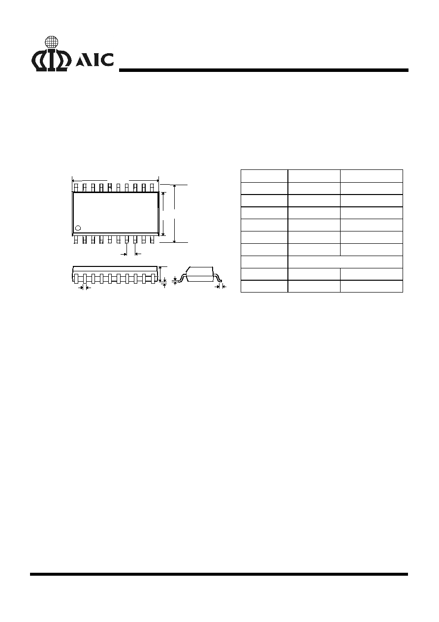
PHYSICAL DIMENSIONS
20 LEAD PLASTIC SO (300 mil) (unit: mm)
SYMBOL
MIN
MAX
A
2.35
2.65
A1
0.10
0.30
B
0.33
0.51
C
0.23
0.32
D
12.60
13.00
E
7.40
7.60
e
1.27(TYP)
H
10.00
10.65
e
B
A
A
1
D
C
E
H
L
L
0.40
1.27