AIC1577
External NMOS Step-Down PWM Controller
FEATURES
N-Channel MOSFET Drive
Operating Input Voltage from 4.5V to 24V
Wide Ouput Range : 0.8V to 20V
±1.5% 0.8V Reference
Low Dropout Operation : 95% Duty Cycle
500KHz Fixed Constant Frequency
Low Standby Current, I
Q
Typically 720
µA
Logic-Control Micropower Shutdown
Output Overvoltage Protection
Internal Diode for Bootstrapped Gate Drive
Current Mode Operation for Excellent Line and
Load Transient Response
Available in an 8-Lead SO and MSOP Package
APPLICATIONS
LCD Monitor
Palmtop Computers, PDAs
Wireless Modems
On-Card Switching Regulators
DC Power Distribution Systems
DESCRIPTION
The AIC1577 is a current mode switching
regulator controller that drives external N-
channel power MOSFET using a fixed fre-
quency architecure. It uses external divider to
adjust output voltage from 0.8V to 20V with
excellent line and load regulation. A maximum
high duty cycle limit of 95% provides low
dropout operation which extends operating
time in battery-operated systems.
Switching frequency up to 500KHz are
achievable thus allowing smaller sized filter
components. The operating current level is
user-programmable via an external current
sense resistor. It also provide output overvolt-
age protection under fault conditions.
A multifunction pin (I
TH
/RUN) allows external
compensation for optimum load step re-
sponse plus shutdown. Soft start can also be
implemented with this pin to properly se-
quence supplies. Package available are in
SOP8 and MSOP8 for SMD.
Analog Integrations Corporation
Si-Soft Research Center
DS-1577P-02 010405
3A1, No.1, Li-Hsin Rd. I , Science Park , Hsinchu 300, Taiwan , R.O.C.
TEL: 886-3-5772500
FAX: 886-3-5772510
www.analog.com.tw
1

AIC1577
TYPICAL APPLICATION CIRCUIT
V
IN
6V~24V
+
C
IN1
22
µF
R
S
33m
M1
FDS6694
C3
0.1
µF
D1
SL43
L1
10
µH
V
OUT
3.3V 3A
C1
1000pF
C5
330pF
R3
24k
R2
62k
R1
20k
VIN
8
ITH/RUN
2
FB
3
GND
4
SW
5
DRI
6
BOOST
7
CS
1
AIC1577
+
C
IN2
22
µF
C2
0.1
µF
C
OUT
220
µF
C4
1nF
C6
2.2
µF
C
IN1
, C
IN2
: HER-MEI 22
µF/35V Electrolytic capacitors
M1: FAIRCHILD FDS6694 N-MOSFET
D1: GS SL43
L1: TDK SLF12555T-100M3R4
C
OUT
: HER-MEI 220
µF /16V Electrolytic capacitor
C6: TAIYO YUDEN LMK212BJ225KG-T Ceramic capacitor
ORDERING INFORMATION
AIC1577-XXXX
PACKING TYPE
TB: TUBE
TR: TAPING & REEL
PACKAGING TYPE
S: SMALL OUTLINE
O: MSOP8
C: Commercial
P: Lead Free Commercial
Example: AIC1577COTR
in MSOP Package & Taping & Reel
Packing Type
AIC1577POTR
in MSOP Lead Free Package &
Taping & Reel Packing Type
PIN CONFIGURATION
TOP VIEW
DRI
VIN
BOOST
SW
FB
I
TH
/RUN
GND
CS 1
3
4
2
8
6
5
7
2

AIC1577
ABSOLUTE MAXIMUM RATINGS
Supply Voltage (VIN)
25V
Drive Supply Voltage (BOOST)
32V
Switch Voltage (SW)
25V
Differential Boost Voltage (BOOST to SW )
8V
I
TH
/RUN,VFB Voltages
7V
Peak Drive Output Current < 10
µS (DRI )
2A
Operating Temperature Range
-40
∞C ~ 85∞C
Junction Temperatrue
125
∞C
Storage Temperature Range
-65
∞C ~ 150∞C
Lead Temperature (Soldering. 10 sec)
260
∞C
Thernal Resistance (
JA
) (Assume No Ambient Airflow, No Heatsink)
DIP8
100
∞C/W
SOP8
160
∞C/W
MSOP8
180
∞C/W
Absolute Maximum Ratings are those values beyond which the life of a device may be
Impaired.
TEST CIRCUIT
Refer to Typical Application Circuit.
ELECTRICAL CHARACTERISTICS
(T
A
=25
∞C, V
IN
=15V, unless otherwise noted.) (note1)
PARAMETER
TEST CONDITIONS
MIN.
TYP.
MAX. UNIT
Input Voltage
4.5
24
V
Normal Mode (Note 2)
720
900
µA
Input Supply Current
Shutdown Mode, V
ITH/RUN
=0V
16
20
µA
Feedback
Voltage
0.788 0.8 0.812
V
Output Overvoltage Lockout V
FB
connect to Vout, V
OVL
=V
OVL
-
V
FB
20 55 90
mV
Reference Voltage Line
Regulation
V
IN
= 4.5V to 20 V
0.002
0.015
%/V
Output Voltage Load Regula-
tion
I
TH
Sinking 5
µA
I
TH
Sourcing 5
µA
0.7
-0.4
1.1
-0.8
%
Run Threshold
0.6
0.8
0.9
V
Maximum Current Sense
Threshold
V
FB
=0.72V
125 150 175 mV
Oscillator
Frequency
450 500 550 KHz
3

AIC1577
ELECTRICAL CHARACTERISTICS
(Continued)
PARAMETER
TEST CONDITIONS
MIN.
TYP.
MAX. UNIT
DRI Rise Time
C
LOAD
= 3000
P
F
50
75
nS
DRI Fall Time
C
LOAD
= 3000
P
F
50
75
nS
BOOST Voltage
V
IN
=8V, I
BOOST
=5mA,
SW=0V
4.9 5.3 5.7 V
Maximum Duty Cycle
90
94
%
Soft Start Time
5
7.5
mS
Run Current Source
V
ITH/RUN
=0V, V
FB
=0V
1.0 2.3 4.0
µA
Run Pullup Current
V
ITH/RUN
=1V
100 190 250
µA
Note 1: Specifications are production tested at TA=25
∞C. Specifications over the -40∞C to 85∞C operating
temperature range are assured by design, characterization and correlation with Statistical Quality
Controls (SQC).
Note 2: Dynamic supply current is higher due to the gate charge being delivered at the switching frequency.
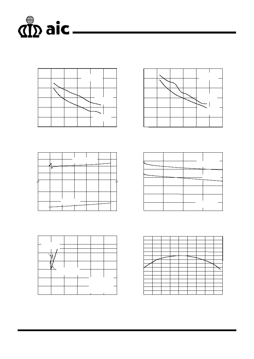
TYPICAL PERFORMANCE CHARACTERISTICS
1
10
100
1000
10000
70
75
80
85
90
95
100
V
IN
=6V
E
f
ficienc
y
(
%
)
Load Current (mA)
V
IN
=12V
V
IN
=19V
V
OUT
=3.3V
Fig. 1 Efficiency vs Load Current (V
OUT
=3.3V)
E
f
ficienc
y
(
%
)
Load Current (mA)
Fig. 2 Efficiency vs Load Current (V
OUT
=5.0V)
1
10
100
1000
10000
70
75
80
85
90
95
100
V
OUT
=5V
V
IN
=6V
V
IN
=12V
V
IN
=19V
4
AIC1577
TYPICAL PERFORMANCE CHARACTERISTICS
(Continued)
Efficienc
y
(%)
Input Voltage (V)
Fig. 3 Efficiency vs Input Voltage
0
5
10
15
20
25
30
70
75
80
85
90
95
100
V
OUT
=3.3V
I
LOAD
=1A
I
LOAD
=0.1
A
Efficienc
y
(
%
)
Input Voltage (V)
Fig. 4 Efficiency vs Input Voltage
0
5
10
15
20
25
30
70
75
80
85
90
95
100
V
OUT
=5V
I
LOAD
=1A
I
LOAD
=0.1A
S
u
pp
l
y
C
u
r
r
en
t
(
µ
A)
Input Voltage (V)
Fig. 5 Supply Current vs Input Voltage
0
5
10
15
20
25
30
0
20
40
500
600
700
800
900
Normal Mode
Shutdown
B
oos
t V
o
lta
g
e
(
V
)
Boost Load Current (mA)
Fig. 6 Boost Load Regulation
0
V
CC
=5V
V
CC
=15V
V
PHASE
=0V
0
5
10
15
20
1
2
3
4
5
6
7
B
oos
t V
o
lta
ge (V
)
Input Voltage (V)
Fig. 7 Boost Line Regulation
I
BOOST
=2mA
V
PHASE
=0V
0
5
10
15
20
25
30
1
3
5
7
0
2
4
6
VCC DOWN
VCC UP
R
e
ferenc
e V
o
lta
g
e
(
V
)
Temperature (
∞C)
Fig. 8 Reference Voltage vs Temperature
-40
-20
0
20
40
60
80
100
120
140
0.790
0.791
0.792
0.793
0.794
0.795
0.796
0.797
0.798
0.799
0.800
0.801
0.802
0.803
0.804
0.805
5