þÿ

AIC1579/L
Step-Down DC/DC Controller
Analog Integrations Corporation
4F, 9 Industry E. 9th Rd, Science-Based Industrial Park, Hsinchu, Taiwan
DS-1579-02 012102
TEL: 886-3-5772500
FAX: 886-3-5772510
www.analog.com.tw
1
n
FEATURES
l
Operation Voltage up to 15V.
l
Simple Voltage-Mode PWM Control.
l
Fast Transient Response.
l
2V and 1.3V
±
2% Feedback Voltage Reference
Option.
l
Adjustable Current Limit without External Sense
Resistors.
l
200KHz Typical Switching Frequency.
l
Short-Circuit Protection with Low Short Circuit
Output Current.
n
APPLICATIONS
l
Power Supply for Motherboard V
GTL
(1.5V Output)
l
Power Supply for Motherboard V
I/O
.
l
High-Power 5V to 3.xV DC/DC Regulators.
l
Low-Voltage Distributed Power Supplies.
n
DESCRIPTION
The AIC1579 is a high-power, high-efficiency
voltage-mode DC/DC controller for motherboard
V
I/O
power supply applications. Designed to
drive an N-channel MOSFET in a standard buck
topology, the AIC1579 features a high voltage
CMOS output driver, short-circuit protection,
and 8-pin package.
An external 4-bit Digital-to-Analog Converter
(DAC) can be used along with the AIC1579 to
adjust the output voltage from 2.0V to 3.5V in
0.1V increments. Table 1 on the following page
specifies the corresponding output voltage for
16 combinations of DAC inputs as in the typical
application circuit.
The 200KHz switching frequency allows for
using small external components while
maintaining high conversion efficiency. The
11MHz bandwidth and 6V/
µ
S slew rate of the
error amplifier ensures high converter
bandwidth and fast transient response.
The AIC1579 provides adjustable overcurrent
and short-circuit protections by sensing the
output current across the on resistance of the
external N-channel MOSFET rather than an
external low value sense resistor.
The AIC1579L provides lower reference voltage
(1.30V) than the default (2.00V, AIC1579) for
lower V
OUT
requirement.
AIC1579/L
2
n
ORDERING INFORMATION
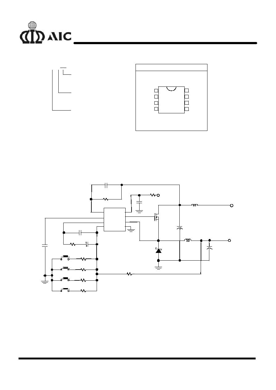
PIN CONFIGURATION
SO-8
TOP VIEW
PHASE
1
3
4
2
VCC
SS
COMP
FB*
UGATE
GND
8
6
5
7
OCSET
*AIC1579: 2.00V
AIC1579L: 1.30V
PACKING TYPE
TR: TAPE & REEL
TB: TUBE
PACKAGING TYPE
N: PLASTIC DIP
S: SMALL OUTLINE
REFERENCE
VOLTAGE
DEFAULT: 2.00V
L: 1.30V
AIC1579XCXXX
Example: AIC1579CSTR
à
2.00V Version in SO-8 Package &
Taping & Reel Packing Type
(CN is not available in TR packing)
n
TYPICAL APPLICATION CIRCUIT
AIC1579
OCSET
COMP
FB
GND
PHASE
SS
UGATE
VCC
C7
1000pF
C6
33P
C2
1000pF
+
C4
1000
µ
F x 6
+
C3
1000
µ
Fx2
R3
3.01K
R2
90.9K 1%
R1
2.2K
7
µ
H
L1
1
µ
H
D1
BYV118
M1
CEB6030L
5V
3.3V/10A
1%
R4
1%
*C1 MUST BE VERY CLOSE TO VCC PIN
C1*
1
µ
F
12V
L2
V
OUT
VID2
VID3
VID1
VID0
R7
7.5K
R6
15.0K
R5
30.1K
60.4K 1%
1%
1%
1%
10
R8
C5
100N
Switching Regulator Circuit
AIC1579/L
3
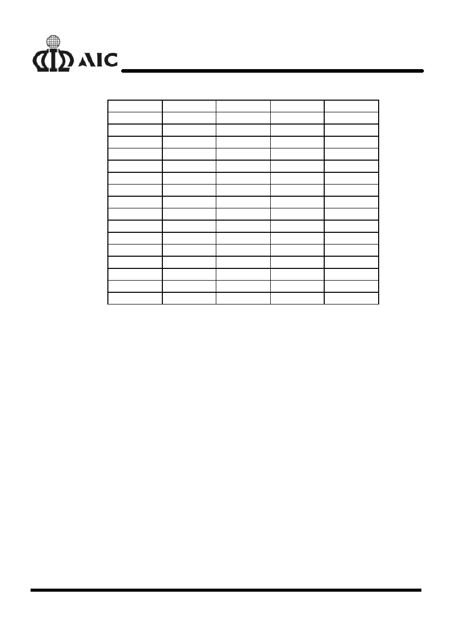
Table 1. Output Voltage Program
VID3
VID2
VID1
VID0
VOUT
1
1
1
1
2.00V
1
1
1
0
2.10V
1
1
0
1
2.20V
1
1
0
0
2.30V
1
0
1
1
2.40V
1
0
1
0
2.50V
1
0
0
1
2.60V
1
0
0
0
2.70V
0
1
1
1
2.80V
0
1
1
0
2.90V
0
1
0
1
3.00V
0
1
0
0
3.10V
0
0
1
1
3.20V
0
0
1
0
3.30V
0
0
0
1
3.40V
0
0
0
0
3.50V
n
ABSOLUTE MAXIMUM RATINGS
Supply Voltage, V
CC
....... ...... ... ... ............................... ... ... ... ......................................... 15V
Input, Output, or I/O Voltage .................. ... ... ... ... ... ....... ... ......... GND - 0.3V to VCC+0.3V
ESD Classification ................................ ... ... ... ........ ... ................. ... ......................... Class 2
Recommended Operating Conditions
Supply Voltage, V
CC
....... ......................... ... ... ... .......... ... ... .................................. 12V
±
10%
Ambient Temperature Range .... ................................... ... ... ... .... ... ... .................. 0
°
C~70
°
C
Junction Temperature Range ....... ............... ... ... ............ ..... ... ......................... 0
°
C~ 100
°
C
Thermal Information
Thermal Resistance,
JA
(Typical, Note 1)
SOIC Package .................................. ... ... ... ... ... ... ... ... ..... ... ... ... ... ........... . 100
°
C/W
SOIC Package (with 3 in
2
of Copper) ... ... ... ... ... ... ... ... ... ... ... ... ... ... ......... .. 90
°
C/W
Maximum Junction Temperature (Plastic Package) ... ... ... .... ... ..... ... ... ................... 150
°
C
Maximum Storage Temperature Range ... ... ... ... ..... ... ... ... ......... ... .... ......... 65
°
C~150
°
C
Maximum Lead Temperature (Soldering 10 Sec) ... ... ... ... ... ... ... ...... ... ......... ......... 300
°
C
Note 1:
JA
is measured with the component mounted on an evaluation PC board in free air.
n
TEST CIRCUIT
Refer to TYPICAL APPLICATION CIRCUIT.
AIC1579/L
4
n
ELECTRICAL CHARACTERISTICS
(VCC=12V, T
A
=25
°
C, unless otherwise
specified.)
PARAMETER
TEST CONDITIONS
SYMBOL
MIN.
TYP.
MAX.
UNIT
VCC Supply Current
Nominal Supply
UGATE Open
I
VCC
2.3
mA
Power-On Reset
V
CC
Threshold
V
OCSET
=4.5V
10.4
V
Oscillator
Frequency
175
200
225
KHz
Max. Duty Cycle
100
%
Internal Reference Voltage
Reference Voltage
AIC1579
AIC1579L
1.96
1.27
2.00
1.30
2.04
1.33
V
Error Amplifier
DC Gain
76
dB
Gain-Bandwidth Product
GBW
11
MHz
Slew Rate
SR
6
V/
µ
S
Gate Driver
Upper Gate Source
R
UGATE
8
12
Upper Gate Sink
R
UGATE
5.5
10
Protection
OCSET Current Source
V
OCSET
=4.5VDC
I
OCSET
170
200
230
µ
A
SS Current
I
SS
10
µ
A
n
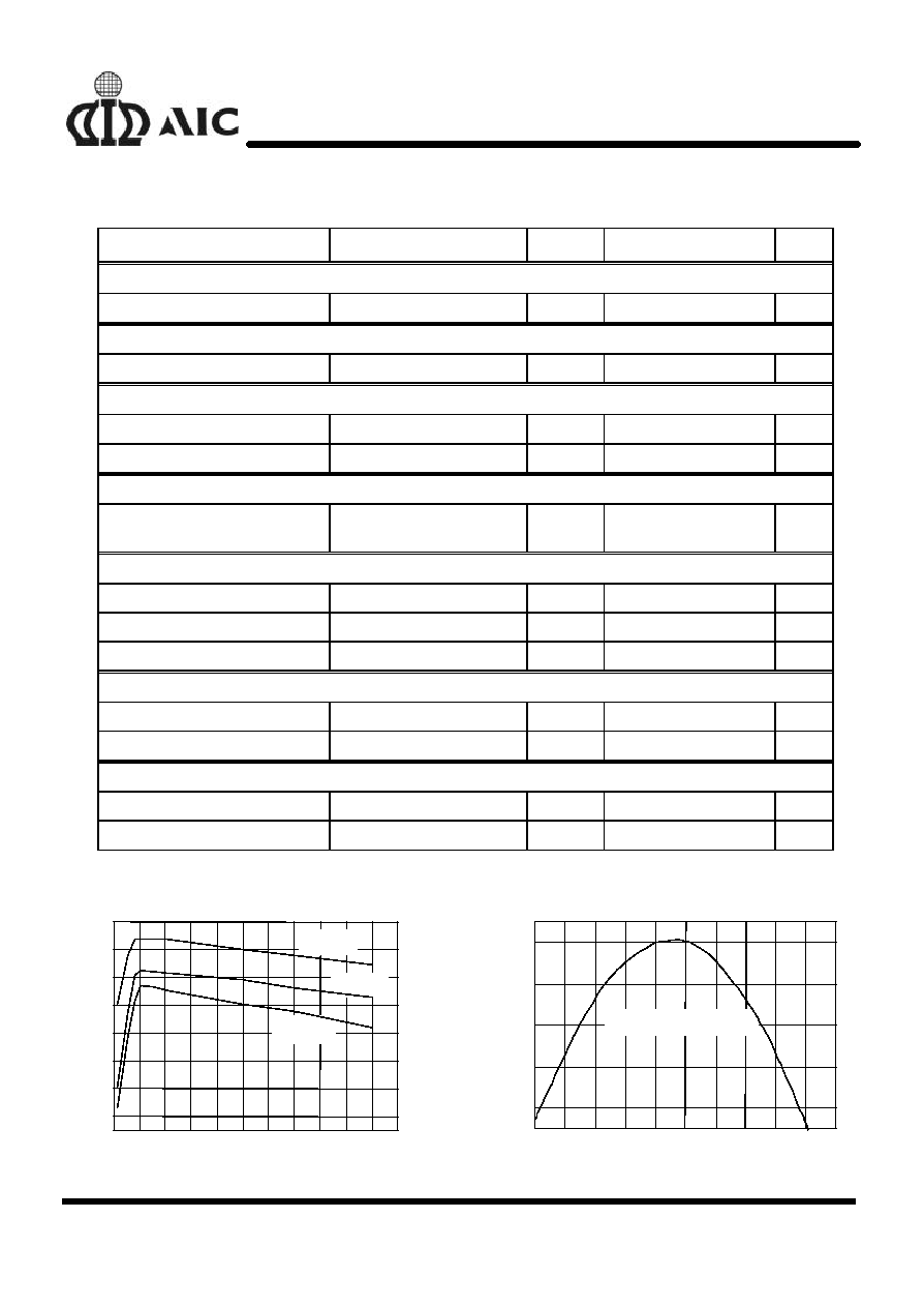
TYPICAL PERFORMANCE CHARACTERISTICS
1
2
3
4
5
6
7
8
9
10 11
30
40
50
60
70
80
90
100
Vo=3.5V
Vo=2.0V
Vo=1.3V
Efficiency (%)
I
OUT
(A)
Fig. 1 Efficiency vs. Load Current
OCSET Current
(
µ
A)
Temperature (
°
C)
Fig. 2 OCSET Current vs. Temperature
-40 -20
0
20
40
60
80
100 120 140 160
192
194
196
198
200
Tc=134ppm/ C@ 0~100
°
C
AIC1579/L
5
n
TYPICAL PERFORMANCE CHARACTERISTICS(
Continued
)
Soft Start (
µ
A)
Temperature (
°
C)
Fig. 3 Soft-Start Current vs. Temperature
-40
-
20
0
20
40
60
80
100
120 140 160
9.3
9.4
9.5
9.6
9.7
9.8
9.9
Tc = 306 ppm/
°
C @ 0~100
°
C
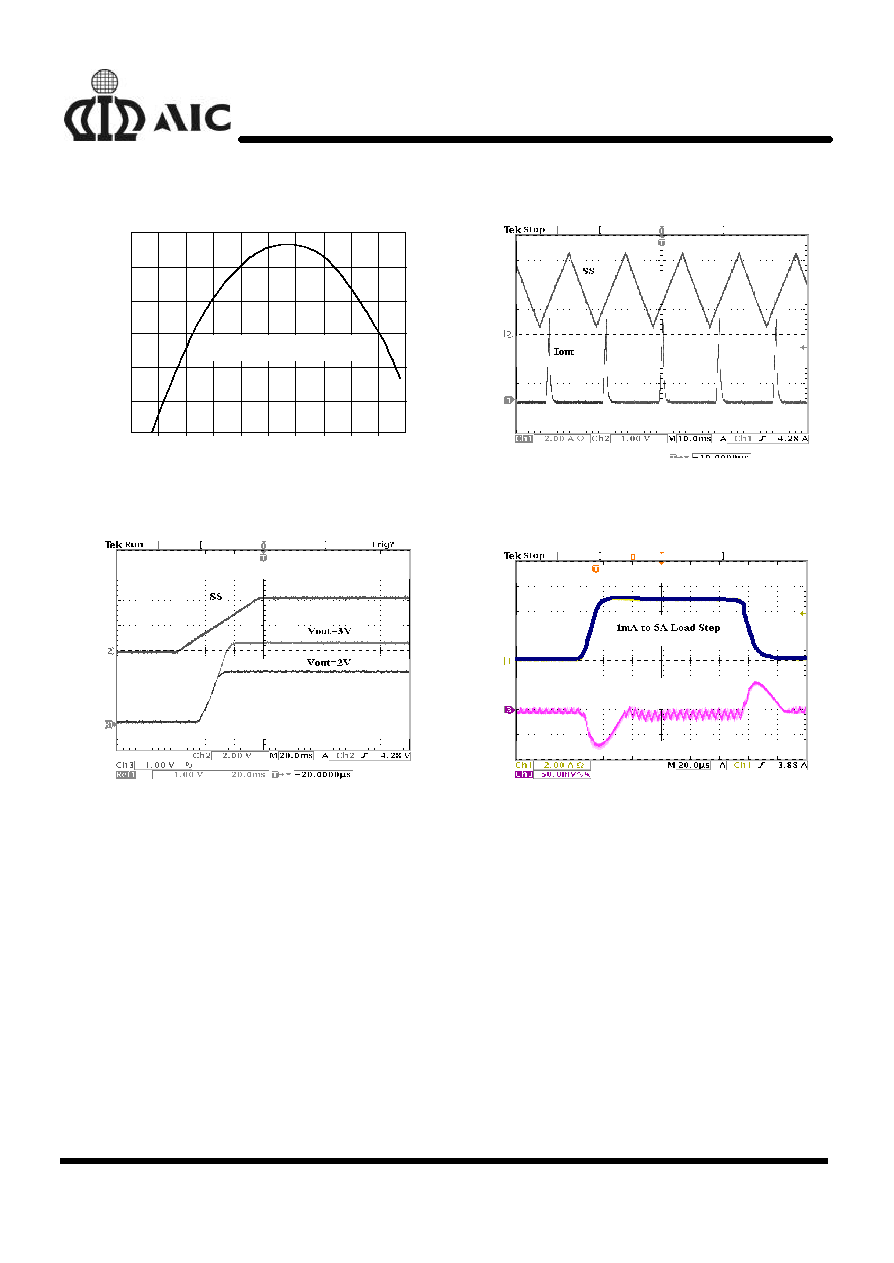
Fig. 4 Over-Current Operation
Fig. 5 Soft Start Initiates Output
Fig. 6 Transient Response
AIC1579/L
6
n
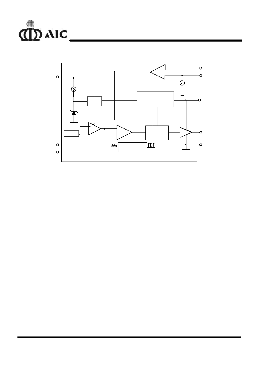
BLOCK DIAGRAM
-
+
-
+
4V
Soft
Start
Error
AMP
VCC
200
µ
A
Over Current Comparator
PHASE
OCSET
10
µ
A
SS
COMP
UGATE
GND
FB
PWM Comparator
REF.
Power-ON Reset
Gate
Control
Oscillator
n
PIN DESCRIPTIONS
PIN 1: OCSET- Current limit sense pin. Connect
a resistor R
OCSET
from this pin to
the drain of the external
MOSFET. R
OCSET
, an internal
200
µ
A current source (I
OCSET
),
and the external MOSFET on-
resistance (R
DS(ON)
) jointly set the
overcurrent trip point according
to the following equation:
)
ON
(
DS
OCSET
OCSET
PEAK
R
R
I
I
×
=
If FB pin voltage is sensed to be
below 50% of the internal
voltage reference VDAC, the
overcurrent comparator cycles
the soft-start function.
PIN 2: SS
- Soft start pin. Connect a
capacitor from this pin to ground.
An internal 10
µ
A current source
provides soft start function for
the converter.
PIN 3: COMP - External compensation pin. This
pin is connected to error
amplifier output and PWM
comparator. A RC network is
connected to FB pin to
compensate the voltage-control
feedback loop of the converter.
PIN 4: FB
- The error amplifier inverting
input pin. The FB pin and COMP
pin are used to compensate the
voltage-control feedback loop.
)
R4
R3
(1
*
1.3V
V
OUT
+
=
for
AIC1579L
)
R4
R3
(1
*
2V
V
OUT
+
=
for
AIC1579
Refer to Fig. 7.
PIN 5: GND
- Ground pin.
PIN 6: PHASE - Overcurrent detection pin.
Connect the PHASE pin to
source of the external N-
MOSFET. This pin detects the
voltage drop across the
MOSFET R
DS(ON)
for overcurrent
protection.
AIC1579/L
7
PIN 7: UGATE - External MOSFET gate drive pin.
Connect this pin to gate of the
external MOSFET.
PIN 8: VCC
- The chip power supply pin.
Recommended supply voltage is
12V.
n
APPLICATION CIRCUIT
AIC1579L
OCSET
COMP
FB
GND
PHASE
SS
UGATE
VCC
C7
1000pF
C6
33P
C5
0.01
µ
F
C2
1000pF
+
C4
1000
µ
F x 6
+
C3
1000
µ
FX2
R2
90.9K 1%
R1
2.2K
7
µ
H
L1
1
µ
H
D1
BYV118
M1
CEB6030L
5V
R
3
2K
1%
1
%
*C1 MUST BE VERY CLOSE TO VCC PIN
C1*
1
µ
F
12V
L2
VOUT
1.5V/10A
R
4
13K
1%
*V
OUT
=1.3V x (1+ R3/R4)
10
R8
Fig. 7 DC/DC Buck Converter Circuit
n
PHYSICAL DIMENSIONS
l
8 LEAD PLASTIC SO (unit: mm)
SYMBOL
MIN
MAX
A
1.35
1.75
A1
0.10
0.25
B
0.33
0.51
C
0.19
0.25
D
4.80
5.00
E
3.80
4.00
e
1.27(TYP)
H
5.80
6.20
L
0.40
1.27
D
H
e
A
B
A1
C
E
L
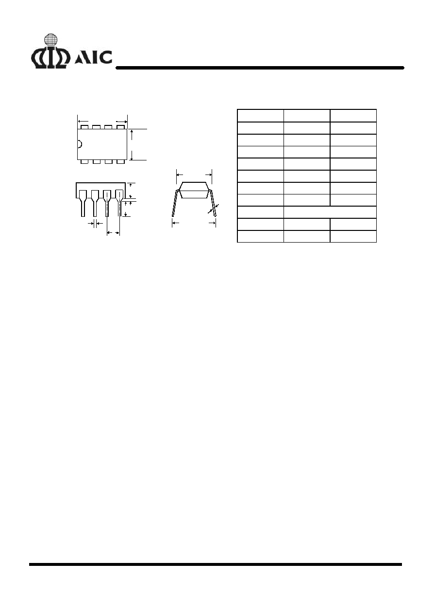
AIC1579/L
8
l
8 LEAD PLASTIC DIP (unit: mm)
SYMBOL
MIN
MAX
A1
0.381
--
A2
2.92
4.96
b
0.35
0.56
C
0.20
0.36
D
9.01
10.16
E
7.62
8.26
E1
6.09
7.12
e
2.54 (TYP)
eB
--
10.92
b
e
L
A2
A1
eB
E
C
E1
D
L
2.92
3.81