
ADVANCED INFORMATION
AIC1596
3A STEP-DOWN PWM REGULATOR
SPEC NO: DS-1596-P1 03/23/00
ANALOG INTEGRATIONS CORPORATION
www.analog.com.tw
4F, 9 Industry E. 9th Road, Science-based Industrial Park , Hsinchu, Taiwan, R.O.C. TEL: (8863)577-2500 FAX:(8863)577-2510
1
!
FEATURES
"
Operating Input Voltage From 4.5V to 36V
"
2.5V, 3.3V, 5V , 12V and Adjustable Output Ver-
sion
"
Adjustable Version Output Voltage Range , 1.25V
to 30V
±
4% max Over Line and Load Regulation
"
Available in TO220-5 and TO263-5 Package
"
Requires Only 4 External Components.
"
150KHz/300KHz Fixed Constant Frequency
"
Low Power Standby Mode, I
Q
Typically 80
µ
A
"
TTL Shutdown Capability.
"
Output Overvoltage Protection
"
Current Limit and Thermal Shutdown Protection.
"
3A Guaranteed Output Current
!
APPLICATIONS
"
Simple High Efficiency Step-down regulator
"
On-Card Switching regulators
"
Fixed Voltage power supply for LCD Monitor
!
DESCRIPTION
The AIC1596 series are step-down monolithic
PWM regulators delivering 3A at fixed voltages of
2.5V , 3.3V, 5.0V , 12V and using a external di-
vider to adjust output voltage from 1.25V to 30V
with excellent line and load regulation.
Switching frequency up to 150KHz/300KHz are
achievable thus allowing smaller sized filter com-
ponents. Internal current limit and thermal shut-
down circuits provide protection from overloads. It
also provides output overvoltage and short pro-
tection under fault conditions.
The internal precious reference combined with
voltage feedback loop provides optimum output
voltage accuracy and fast load transient response.
Packages available are in standard TO220-5 for
standard assembly and TO263-5 for SMD.
!
TYPICAL APPLICATION CIRCUIT
L1
R1
R2
+
C3
+
C1
C2
D1
V
OUT
V
IN
IN
1
SHDN
5
OUT
2
FB
4
3
GND
AIC1596
R1 short and R2 open for fixed
switching output version
3A Precision PWM DC/DC Regulator

AIC1596
3A STEP-DOWN PWM REGULATOR
SPEC NO: DS-1596-P1 03/23/00
ANALOG INTEGRATIONS CORPORATION
www.analog.com.tw
4F, 9 Industry E. 9th Road, Science-based Industrial Park , Hsinchu, Taiwan, R.O.C. TEL: (8863)577-2500 FAX:(8863)577-2510
2
!
ORDERING INFORMATION
PACKAGE TYPE
M: TO263-5
T: TO220-5
OUTPUT VOLTAGE
DEFAULT: Adj.
25: 2.5V
33: 3.3V
50: 5.0V
12: 12.0V
FREQUENCY VERSION
A: 150KHZ
B: 300KHZ
ORDER NUMBER
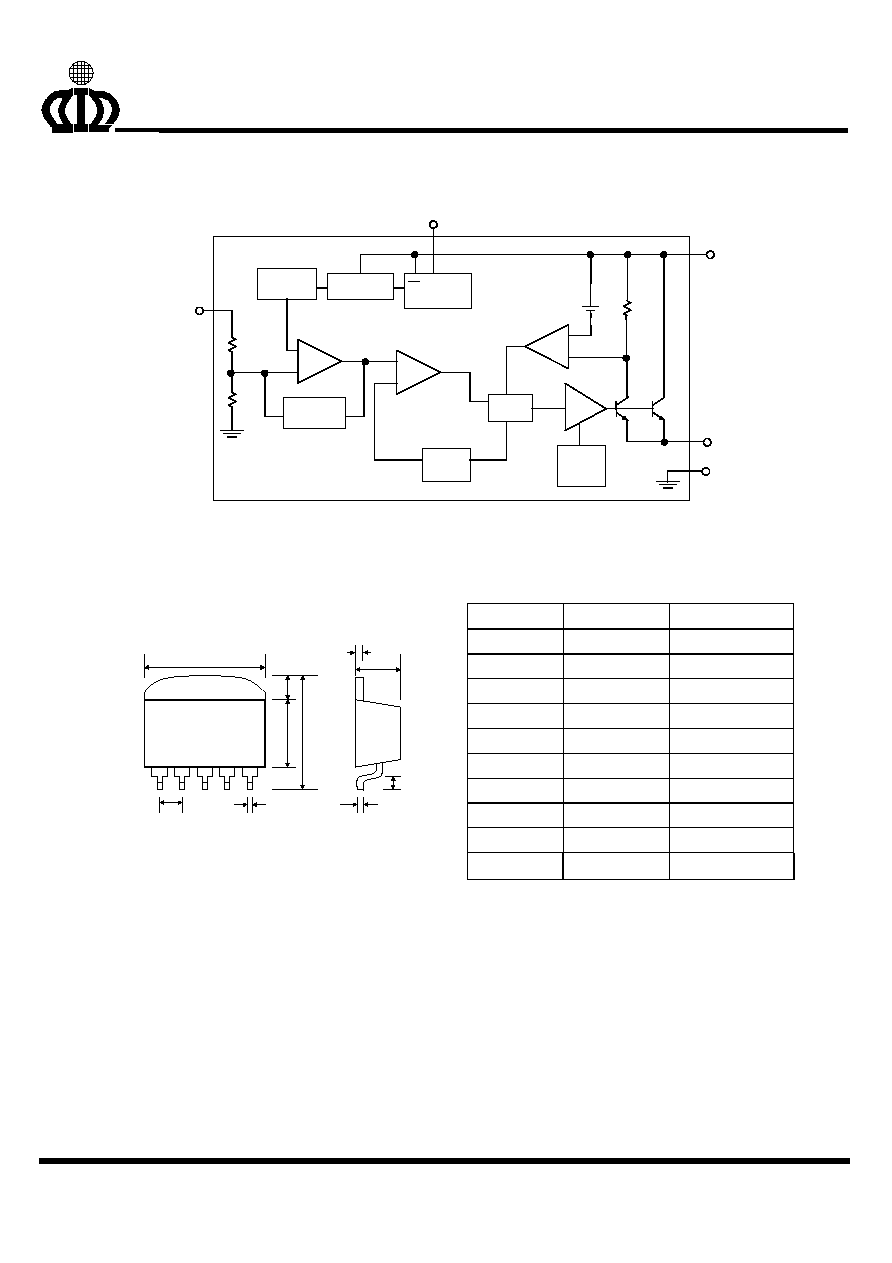
PIN CONFIGURATION
AIC1596X- XXCX
AIC1596A(B)CM
AIC1596A(B)-25CM
AIC1596A(B)-33CM
AIC1596A(B)-50CM
AIC1596A(B)-12CM
(TO263-5)
FRONT VIEW
1: IN
2. OUT
3. GND
4. FB
5. SHDN
AIC1596A(B)CT
AIC1596A(B)-25CT
AIC1596A(B)-33CT
AIC1596A(B)-50CT
AIC1596A(B)-12CT
(TO220-5)
1 2 3 4 5
FRONT VIEW
1: IN
2. OUT
3. GND
4. FB
5.
SHDN
1 2
4 5
3
!
ABSOLUTE MAXIMUM RATINGS
Supply Voltage ...................................................................................................36V
FB, SHDN Pin Input Voltage.................................................................................25V
Operating Temperature Range ................................................................. 0
∞
C ~ 70
∞
C
Storage Temperature Range .............................................................. ≠65
∞
C ~ 150
∞
C
!
TEST CIRCUIT
Refer to Typical Application Circuit.
AIC1596
3A STEP-DOWN PWM REGULATOR
SPEC NO: DS-1596-P1 03/23/00
ANALOG INTEGRATIONS CORPORATION
www.analog.com.tw
4F, 9 Industry E. 9th Road, Science-based Industrial Park , Hsinchu, Taiwan, R.O.C. TEL: (8863)577-2500 FAX:(8863)577-2510
3
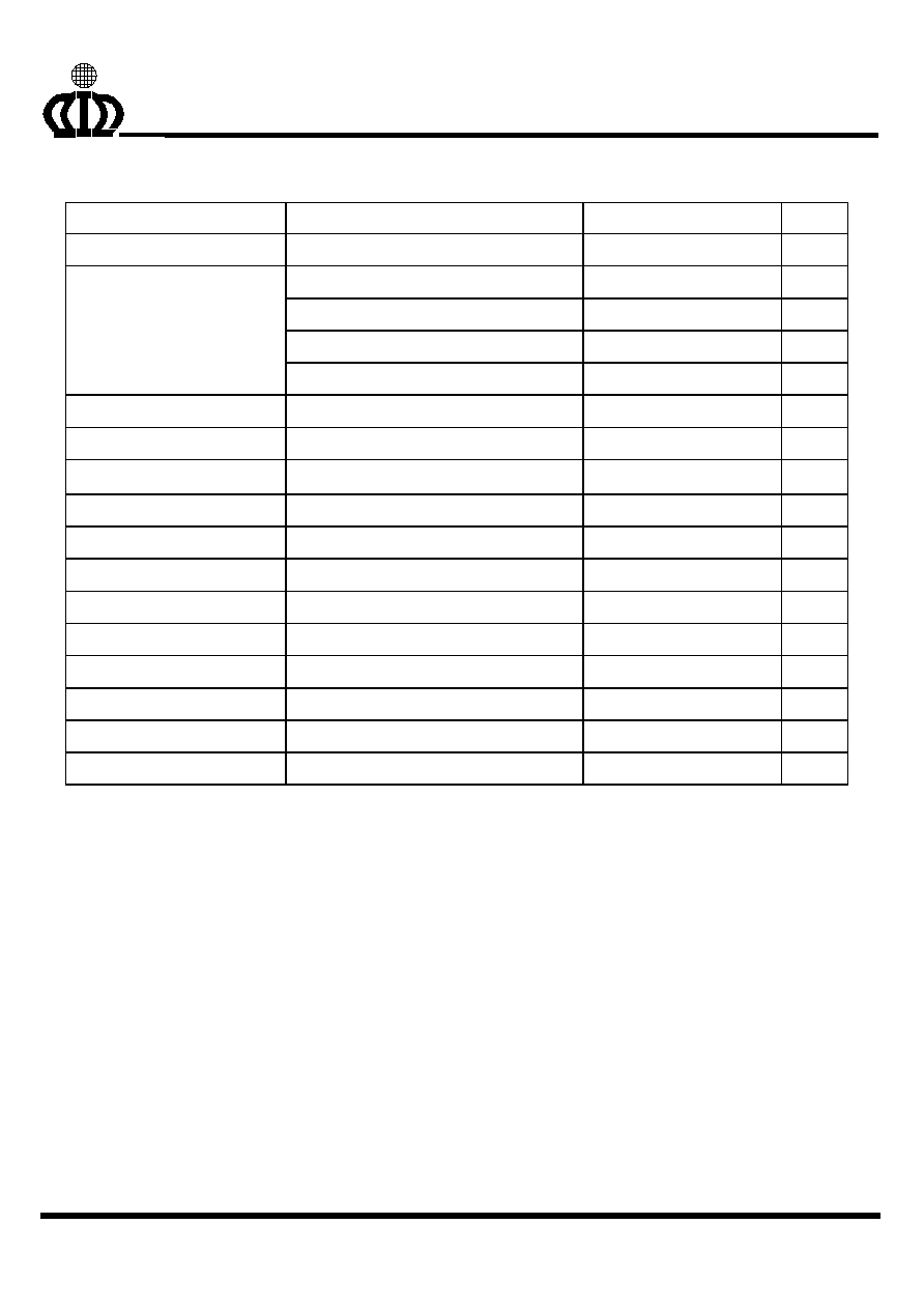
ELECTRICAL CHARACTERISTICS
(T
J
=25
∞
∞
∞
∞
C, V
IN
=18V)
PARAMETER
TEST CONDITIONS
MIN.
TYP.
MAX.
UNIT
Input Voltage
4.5
36
V
AIC1596-25 (V
IN
> 4.5V)
2.5
V
AIC1596-33 (V
IN
> 4.5V)
3.3
V
AIC1596-50 (V
IN
> 7.0V )
5.0
V
Fixed Output Voltage
AIC1596-12 (V
IN
> 15V )
12.0
V
Feedback Voltage
AIC1596 Adjustable
1.25
V
Output Voltage Regulation
4
%
Quiescent Current
Internal switch off
1
5
mA
Shutdown Quiescent Current
SHDN = 5V (OFF)
80
µ
A
Logic Input High
(Regulator OFF)
2
V
Logic Input Low
(Regulator ON )
0.8
V
Oscillator Frequency
AIC1596A series
150
Oscillator Frequency
AIC1596B series
300
KHz
Output Current Limit
3.0
A
Over Voltage Protection
120
%
Maximum Duty Cycle
100
%
Efficiency
Vo=5V , Io=3A
90
%
!
PIN DESCRIPTIONS
PIN 1: IN Supply voltage input for the IC
switching regulator. A suitable input
bypass capacitor must be present at
this pin to minimize voltage transients
and to supply the switching currents
needed by the regulator.
PIN 2:OUT
Internal switch. The voltage at this pin
switches between (V
IN
-V
SAT
) and ap-
proximately ≠0.5V, with a duty cycle of
approximately V
OUT
/V
IN
.
PIN 3: GND
Ground requires a short, low noise
connection to ensure good load
regulation.
PIN 4: FB
Feedback input for fixed-output or
adjustable-output version. Connect di-
rectly to output for fixed operation
version or to a resistor divider for ad-
justable operation versions.
PIN 5: SHDN Allows the switching regulator circuit
to be shutdown using logic level sig-
nals thus dropping the total input sup-
ply current to approximately 80
µ
A.
Drive it high to disable the reference,
control circuitry and internal switches.
Drive low or connect to GND for nor-
mal operation.
AIC1596
3A STEP-DOWN PWM REGULATOR
SPEC NO: DS-1596-P1 03/23/00
ANALOG INTEGRATIONS CORPORATION
www.analog.com.tw
4F, 9 Industry E. 9th Road, Science-based Industrial Park , Hsinchu, Taiwan, R.O.C. TEL: (8863)577-2500 FAX:(8863)577-2510
4
!
BLOCK DIAGRAM
IN
FB
OUT
COMP.
COMP.
GND
2.5V Regulator
1.25 V
Reference
Driver
Compensation
Circuit
SHDN
ON / OFF
AMP.
150/300
KHz OSC
Current
Limit
Latch
Thermal
Shutdown
!
PHYSICAL DIMENSIONS
"
TO-263-5L (unit: mm)
SYMBOL
MIN
MAX
A
4.07
4.83
B
1.45
1.96
C
0.36
0.64
C2
1.14
1.40
D
8.63
9.66
E
9.78
10.54
E
0.71
1.02
L
15.11
15.59
L1
2.28
2.80
E
e
L1
L2
L
A
D
C
B
L2
-
1.40
AIC1596
3A STEP-DOWN PWM REGULATOR
SPEC NO: DS-1596-P1 03/23/00
ANALOG INTEGRATIONS CORPORATION
www.analog.com.tw
4F, 9 Industry E. 9th Road, Science-based Industrial Park , Hsinchu, Taiwan, R.O.C. TEL: (8863)577-2500 FAX:(8863)577-2510
5
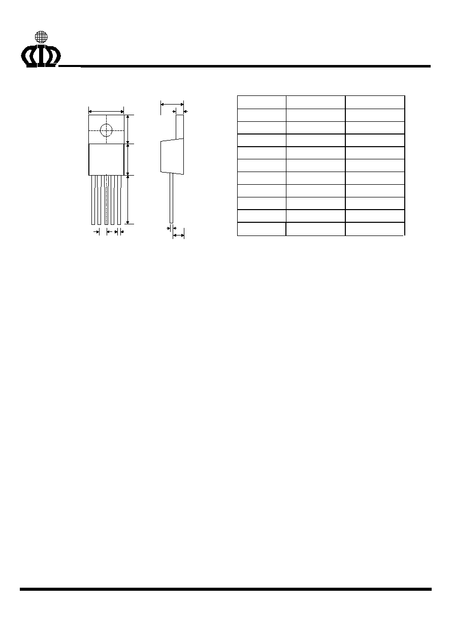
"
TO-220-5 (unit: mm)
SYMBOL
MIN
MAX
A
4.06
4.83
D
8.35
8.89
E
9.78
10.54
e
1.57
1.85
e1
0.76
1.02
e2
0.33
0.64
F
1.14
1.40
H1
5.46
6.86
J1
2.29
3.18
L
13.21
14.73
E
e
L
A
F
H1
D
J1
e2