AIC1610/AIC1611
High Efficiency Synchronous Step-Up DC/DC
Converter
FEATURES
High Efficiency (93% when V
IN
=2.4V,
V
OUT
=3.3V, I
OUT
=200mA)
Output Current up to 500mA. (AIC1610 at
V
IN
=2.4V and V
OUT
=3.3V)
20
µA Quiescent Supply Current.
Power-Saving Shutdown Mode (0.1
µA typical).
Internal Synchronous Rectifier (No External Di-
ode Required).
On-Chip Low Battery Detector.
Low Battery Hysteresis
Space-Saving Package: MSOP-8
APPLICATIONS
Palmtop & Notebook Computers.
PDAs
Wireless Phones
Pocket Organizers.
Digital Cameras.
Hand-Held Devices with 1 to 3-Cell of
NiMH/NiCd Batteries.
DESCRIPTION
The AIC1610/AIC1611 are high efficiency
step up DC-DC converters. The start-up volt-
age is as low as 0.8V with operating voltage
down to 0.7V. Simply consuming 20
µA of qui-
escent current. These devices offer a built-in
synchronous rectifier that reduces size and
cost by eliminating the need for an external
Schottky diode and improves overall effi-
ciency by minimizing losses.
The switching frequency can range up to
500KHz depending on the load and input volt-
age. The output voltage can be easily set by
two external resistors from 1.8V to 5.5V,
connecting FB to OUT to get 3.3V, or con-
necting to GND to get 5.0V. The peak current
of the internal switch is fixed at 1.0A (AIC1610)
or 0.65A (AIC1611) for design flexibility.
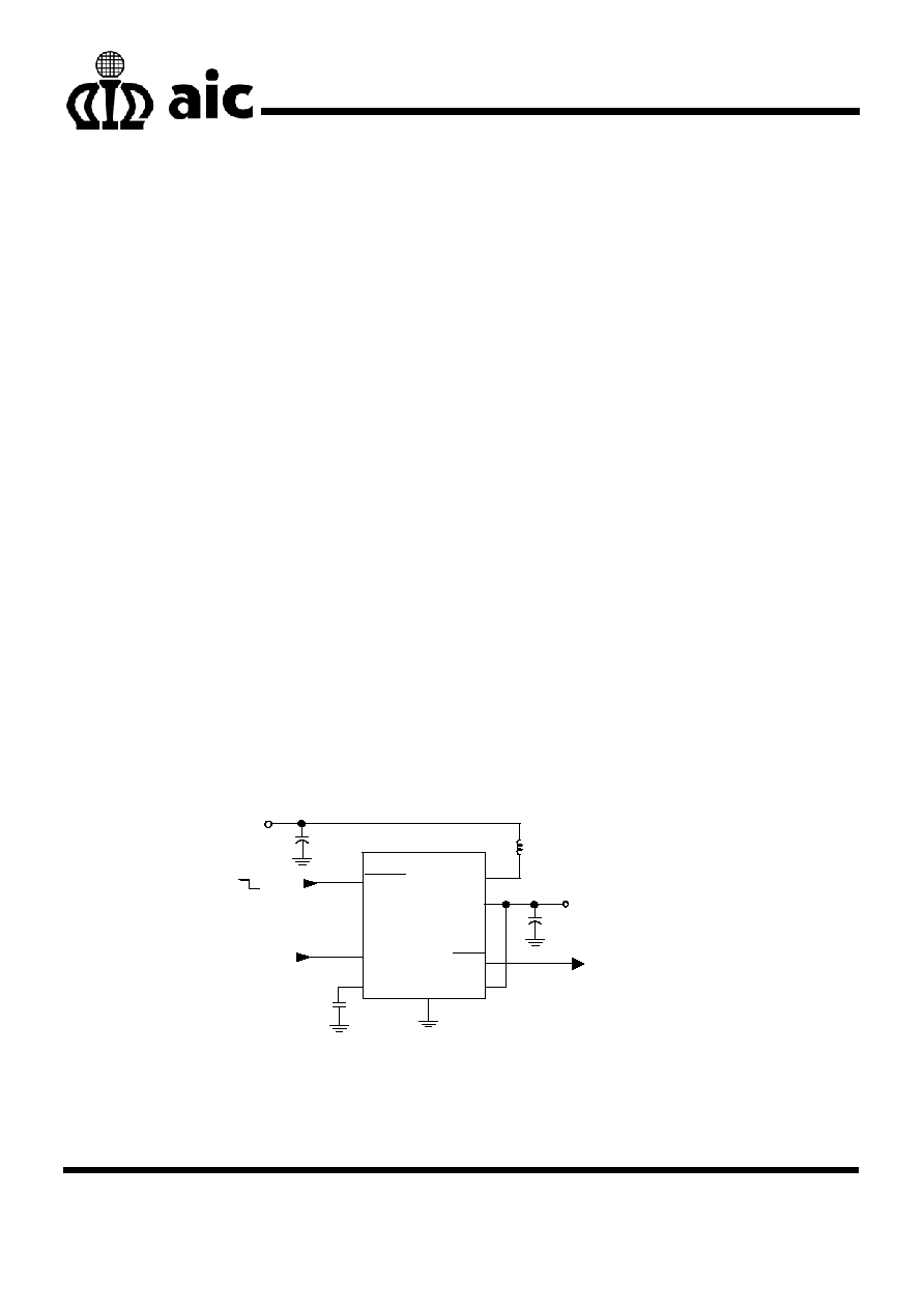
TYPICAL APPLICATION CIRCUIT
Output 3.3V, 5.0V
or Adj. (1.8V to 5.5V)
up to 300mA
Low-battery
Detect Out
AIC1610
AIC1611
OUT
FB
GND
REF
LBO
SHDN
LX
LBI
+
ON
OFF
+
Low Battery
Detection
0.1
µF
V
IN
22
µH
47
µF
47
µF
Analog Integrations Corporation
Si-Soft Research Center
DS-1610P-03 010405
3A1, No.1, Li-Hsin Rd. I , Science Park , Hsinchu 300, Taiwan , R.O.C.
TEL: 886-3-5772500
FAX: 886-3-5772510
www.analog.com.tw
1

AIC1610/AIC1611
ORDERING INFORMATION
AIC1610XX XX
AIC1611XX XX
PIN CONFIGURATION
TOP VIEW
GND
1
3
4
2
8
6
5
7
OUT
LBI
LBO
REF
LX
SHDN
FB
Example: AIC1610COTR
In MSOP-8 Package & Taping &
Reel Packing Type
AIC1610POTR
In MSOP-8 Lead Free Package &
Taping & Reel Packing Type
PACKING TYPE
TR: TAPE & REEL
PACKAGING TYPE
O: MSOP-8
C: COMMERCIAL
P: LEAD FREE COMMERCIAL
ABSOLUTE MAXIMUM RATINGS
Supply Voltage (OUT to GND)
8.0V
Switch Voltage (LX to GND)
V
OUT
+ 0.3V
, LBO to GND
6.0V
SHDN
LBI, REF, FB, to GND
V
OUT
+0.3V
Switch Current (LX)
-1.5A to +1.5A
Output Current (OUT)
-1.5A to +1.5A
Operating Temperature Range
-40
∞C ~ +85∞C
Maximum Junction Temperature
125
∞C
Storage Temperature Range
-65
∞C ~150∞C
Lead Temperature (Soldering 10 Sec.)
260
∞C
Absolute Maximum Ratings are those values beyond which the life of a device may be impaired.
TEST CIRCUIT
Refer to Typical Application Circuit.
2

AIC1610/AIC1611
ELECTRICAL CHARACTERISTICS
(V
IN
=2.0V, V
OUT
=3.3V, FB=V
OUT
, T
A
=25
∞C, unless
otherwise specified.) (Note1)
PARAMETER
TEST CONDITIONS
MIN.
TYP.
MAX.
UNIT
Minimum Input Voltage
0.7
V
Operating
Voltage
1.1 5.5 V
Start-Up Voltage
R
L
=3K
(Note2)
0.8
1.1
V
Start-Up Voltage Tempco
-2
mV/
∞C
Output Voltage Range
V
IN
<V
OUT
1.8 5.5
Output Voltage
FB = V
OUT
3.17
3.3 3.43
V
AIC1610 300
350
FB=OUT
(V
OUT
=3.3V) AIC1611 150
300
AIC1610 180
230
Steady State Output Current
(Note 3)
FB=GND
(
V
OUT
=5.0V) AIC1611 90
160
mA
Reference Voltage
I
REF
= 0
1.199
1.23
1.261
V
Reference Voltage Tempco
0.024
mV/
∞C
Reference Load Regulation
I
REF
= 0 to 100
µA
10
30
mV
Reference Line Regulation
V
OUT
= 1.8V to 5.5V
5
10
mV/V
FB , LBI Input Threshold
1.199
1.23
1.261
V
Internal switch On-Resistance
I
LX
= 100mA
0.3
0.6
AIC1610 0.80
1.0
1.25
LX Switch Current Limit
AIC1611
0.50 0.65 0.85
A
LX Leakage Current
V
LX
=0V~4V; V
OUT
=5.5V
0.05
1
µA
Operating Current into OUT
(Note 4)
V
FB
= 1.4V , V
OUT
= 3.3V
20
35
µA
Shutdown Current into OUT
SHDN = GND
0.1
1
µA
V
OUT
= 3.3V ,I
LOAD
= 200mA
90
Efficiency
V
OUT
= 2V ,I
LOAD
= 1mA
85
%
3

AIC1610/AIC1611
ELECTRICAL CHARACTERISTICS
(Continued)
PARAMETER
TEST CONDITIONS
MIN.
TYP.
MAX.
UNIT
LX Switch On-Time
V
FB
=1V , V
OUT
= 3.3V
2
4
7
µS
LX Switch Off-Time
V
FB
=1V , V
OUT
= 3.3V
0.6
0.9
1.4
µS
FB Input Current
V
FB
= 1.4V
0.03
50
nA
LBI Input Current
V
LBI
= 1.4V
1
50
nA
SHDN Input Current
V
SHDN
= 0 or V
OUT
0.07
50
nA
LBO Low Output Voltage
V
LBI
= 0, I
SINK
= 1mA
0.2
0.4
µA
LBO Off Leakage Current
V
LBO
= 5.5V, V
LBI
= 5.5V
0.07
1
LBI
Hystereisis
50 mV
V
IL
0.2V
OUT
SHDN Input Voltage
V
IH
0.8V
OUT
V
Note 1: Specifications are production tested at T
A
=25
∞C. Specifications over the -40∞C to 85∞C operating tem-
perature range are assured by design, characterization and correlation with Statistical Quality Controls
(SQC).
Note 2: Start-up voltage operation is guaranteed without the addition of an external Schottky diode between the
input and output.
Note 3: Steady-state output current indicates that the device maintains output voltage regulation under load.
Note 4: Device is bootstrapped (power to the IC comes from OUT). This correlates directly with the actual
battery supply.
4
AIC1610/AIC1611
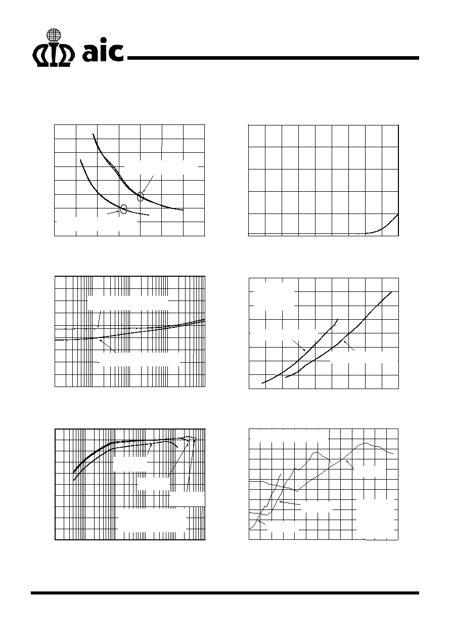
TYPICAL PERFORMANCE CHARACTERISTICS
Input Batter
y
Cur
r
ent (
µ
A)
Input battery voltage (V)
Fig. 1 No-Load Battery Current vs. Input Battery
0.0
0.5
1.0
1.5
2.0
2.5
3.0
3.5
0
20
40
60
80
100
120
140
160
V
OUT
=5V (FB=GND)
V
OUT
=3.3V (FB=OUT)
Sh
u
t
do
wn Cu
rre
nt
Cur
r
ent (
µ
A)
Supply Voltage (V)
Fig. 2 Shutdown Current vs. Supply Voltage
1.0
1.5
2.0
2.5
3.0
3.5
4.0
4.5
5.0
5.5
0.0
0.1
0.2
0.3
0.4
0.5
Fig. 3 Start-Up Voltage vs. Output Current
St
a
r
t
-
U
p
Vo
l
t
a
g
e
(
V
)
0.01
0.1
1
10
100
0.0
0.2
0.4
0.6
0.8
1.0
1.2
1.4
1.6
1.8
V
OUT
=5.0V (FB=GND)
Output Current
(mA)
V
OUT
=3.3V (FB=OUT)
Fig. 4 Turning Point between CCM & DCM
CC
M/D
C
M
B
ound
ar
y O
u
tput
Cur
r
e
n
t
(mA
)
Input Voltage (V)
0.5
1.0
1.5
2.0
2.5
3.0
3.5
4.0
4.5
5.0
0
50
100
150
200
250
300
350
400
V
OUT
=5.0V (FB=GND)
V
OUT
=3.3V (FB=OUT)
L=22
µH
C
IN
=100
µF
C
OUT
=100
µF
Fig. 5 Efficiency vs. Load Current (ref. to Fig.33)
E
f
f
i
c
i
en
cy (%
)
0.01
0.1
1
10
100
1000
0
10
20
30
40
50
60
70
80
90
100
V
IN
=3.6V
Output Current (mA)
V
IN
=2.4V
V
IN
=1.2V
AIC1610 (I
LIMIT
=1A)
V
OUT
=5.0V (FB=GND)
Fig. 6 Ripple Voltage (ref. to Fig.33)
R
i
pp
le V
o
l
t
age
(m
V
)
Output Current (mA)
0
50
100
150
200
250
300
350
400
450 500
550
600
650
0
20
40
60
80
100
120
140
160
180
200
220
V
IN
=2.4V
V
IN
=1.2V
V
OUT
=5.0V
L=22
µH
C
IN
=47
µF
C
OUT
=47
µF
V
IN
=3.6V
AIC1610 (I
LIMIT
=1A)
5