AIC1722A
300mA Low Dropout Linear Regulator
FEATURES
Low Dropout Voltage of 470mV at 300mA Out-
put Current (3.0V Output Version).
Guaranteed 300mA Output Current.
Maximum Input Voltage is 8V
Low Ground Current at 55
µA.
2% Accuracy Output Voltage of 1.8V/ 2.0V
/2.5V /2.7V/ 3.0V/ 3.3V/ 3.5V/ 3.7V/ 3.8V/ 5.0V/
5.2V.
Needs only 1
µF for Stability.
Current and Thermal Limiting.
APPLICATIONS
Voltage Regulator for CD-ROM Drivers.
Voltage Regulator for LAN Cards.
Voltage Regulator for Microprocessor.
Wireless Communication Systems.
Battery Powered Systems.
DESCRIPTION
The AIC1722A is a 3-pin low dropout linear
regulator. The superior characteristics of the
AIC1722A include zero base current loss,
very low dropout voltage, and 2% accuracy
output voltage. Typical ground current
remains approximately 55
µA, from no load to
maximum loading conditions. Dropout voltage
at 300mA output current is exceptionally low.
Output current limiting and thermal limiting are
built in to provide maximal protection to the
AIC1722A against fault conditions.
The AIC1722A comes in the popular 3-pin
SOT-89, TO-92 and SOT-23 packages.
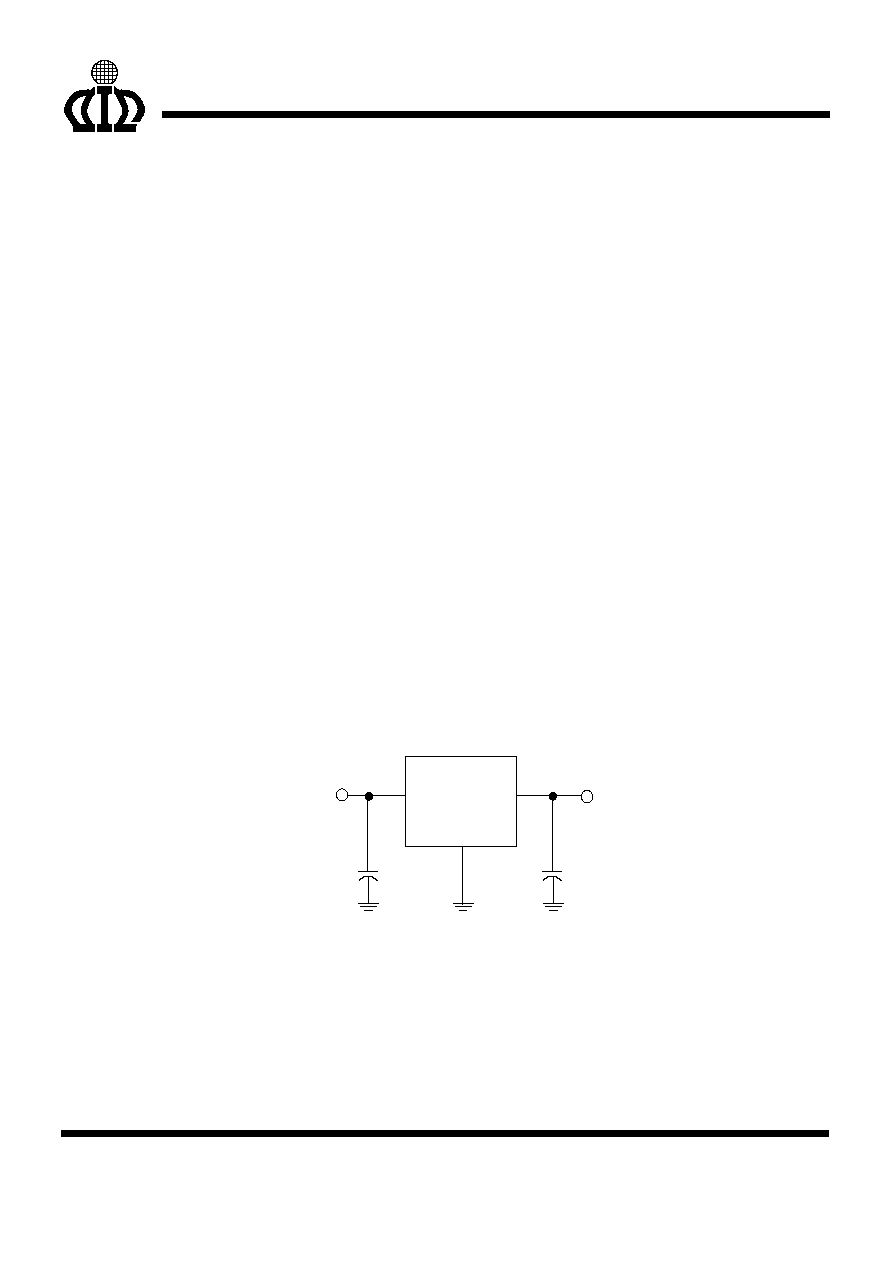
TYPICAL APPLICATION CIRCUIT
+
+
AIC1722A
1
µF
C
OUT
V
OUT
VOUT
GND
VIN
1
µF
C
IN
V
IN
Low Dropout Linear Regulator
(C
IN
and C
OUT
are electrolytic capacitor)
Analog Integrations Corporation
Si-Soft Research Center
DS-1722AP-01 070204
3A1, No.1, Li-Hsin Rd. I , Science Park , Hsinchu 300, Taiwan , R.O.C.
TEL: 886-3-5772500
FAX: 886-3-5772510
www.analog.com.tw
1
AIC1722A
ORDERING INFORMATION
PIN CONFIGURATION
SOT-89 (CXT & PXT)
TOP VIEW
1: VOUT
2. GND
3. VIN
SOT-89 (CXA & PXA)
TOP VIEW
1: GND
2. VIN
3. VOUT
TO-92 (CZT & PZT)
TOP VIEW
1: GND
2. VIN
3. VOUT
TO-92 (CZL & PZL)
TOP VIEW
1: VIN
2. GND
3. VOUT
1
2
3
1
2
3
1
2
3
1
2
3
PACKING TYPE
TR: TAPE & REEL
BG: BAG
PACKAGE TYPE
U: SOT-23
XA: SOT-89
XT: SOT-89
ZT: TO-92
ZL: TO-92
C: Commercial
P: Lead Free Commercial
OUTPUT VOLTAGE
18:
1.8V
20:
2.0V
25:
2.5V
27:
2.7V
30:
3.0V
33:
3.3V
35:
3.5V
37:
3.7V
38:
3.8V
50:
5.0V
52:
5.2V
AIC1722A-XXXXX XX
Example: AIC1722A-18CXATR
1.8V Version, in SOT-89 Package &
Tape & Reel Packing Type
AIC1722A-18PXATR
1.8V Version, in SOT-89 Lead Free
Package & Tape & Reel Packing Type
SOT-23 (CU & PU)
TOP VIEW
1: GND
2: VOUT
3: VIN
3
1
2
SOT-23 MARKING
Part No.
CU
PU
Part No.
CU
PU
AIC1722A-18XU BN18
BN18P
AIC1722A-35XU
BN35
BN35P
AIC1722A-20XU BN20
BN20P
AIC1722A-37XU
BN37
BN37P
AIC1722A-25XU BN25
BN25P
AIC1722A-38XU
BN38
BN38P
AIC1722A-27XU BN27
BN27P
AIC1722A-50XU
BN50
BN50P
AIC1722A-30XU BN30
BN30P
AIC1722A-52XU
BN52
BN52P
AIC1722A-33XU BN33
BN33P
2
AIC1722A
SOT-89 MARKING
Part No.
CXA
PXA
Part No.
CXT
PXT
AIC1722A-18XXA AL18
AL18P
AIC1722A-18XXT BA18
BA18P
AIC1722A-20XXA AL20
AL20P
AIC1722A-20XXT BA20
BA20P
AIC1722A-25XXA AL25
AL25P
AIC1722A-25XXT BA25
BA25P
AIC1722A-27XXA AL27
AL27P
AIC1722A-27XXT BA27
BA27P
AIC1722A-30XXA AL30
AL30P
AIC1722A-30XXT BA30
BA30P
AIC1722A-33XXA AL33
AL33P
AIC1722A-33XXT BA33
BA33P
AIC1722A-35XXA AL35
AL35P
AIC1722A-35XXT BA35
BA35P
AIC1722A-37XXA AL37
AL37P
AIC1722A-37XXT BA37
BA37P
AIC1722A-38XXA AL38
AL38P
AIC1722A-38XXT BA38
BA38P
AIC1722A-50XXA AL50
AL50P
AIC1722A-50XXT BA50
BA50P
AIC1722A-52XXA AL52
AL52P
AIC1722A-52XXT BA52
BA52P
ABSOLUTE MAXIMUM RATINGS
Input Supply Voltage ......................................................................................... -0.3~8V
Operating Temperature Range ................................................................. -40
∞C~ 85∞C
Junction Temperature ................................................................................. 125
∞C
Storage Temperature Range ...................................................................... -65
∞C~150∞C
Lead Temperature (Soldering. 10sec) ............................................................ 260
∞C
Power Dissipation
SOT-89 Package .............................. 0.5W
TO-92
Package
.............................. 0.5W
SOT-23
Package.............................. 0.5W
Absolute Maximum Rating are those value beyond which the life of a device may be impaired.
TEST CIRCUIT
Refer to the TYPICAL APPLICATION CIRCUIT
3
AIC1722A
ELECTRICAL CHARACTERISTICS
(T
A
=25
∞C, C
IN
=1
µF, C
OUT
=1
µF, unless oth-
erwise specified.) (Note 1)
PARAMETER TEST
CONDITIONS
MIN.
TYP.
MAX.
UNIT
No
Load
Output Voltage
AIC1722A-52
AIC1722A-50
AIC1722A-38
AIC1722A-37
AIC1722A-35
AIC1722A-33
AIC1722A-30
AIC1722A-27
AIC1722A-25
AIC1722A-20
AIC1722A-18
V
IN
=8V
-2
+2 %
Line Regulation
I
L
=
1mA,
1.4V
V
OUT
3.2V
3.3V
V
OUT
5.2V
V
IN
=4V~8V
V
IN
=5.5V~8V
3
3
10
15
mV
Load Regulation
(Note 2)
I
L
=0.1~300mA
1.4V
V
OUT
3.9V
4.0V
V
OUT
5.2V
V
IN
=5V
V
IN
=7V
7
15
20
40
mV
Current Limit
(Note 3)
V
IN
=7V, V
OUT
=0V 300
mA
Dropout Voltage
(Note 4)
I
L
=300mA
4.0V
V
OUT
5.2V
3.0V
V
OUT
3.9V
2.5V
V
OUT
2.9V
2.0V
V
OUT
2.4V
1.4V
V
OUT
1.9V
400
470
570
800
1260
mV
Ground Current
I
O
=0.1mA~I
MAX
1.4V
V
OUT
3.9V
4.0V
V
OUT
5.2V
V
IN
=5~8V
V
IN
=7~8V
55
55
80
80
µA
Note 1:
Specifications are production tested at T
A
=25
∞C. Specifications over the -40∞C to 85∞C operating
temperature range are assured by design, characterization and correlation with Statistical Quality
Controls (SQC).
Note 2:
Regulation is measured at constant junction temperature, using pulse testing with a low ON time.
Note 3: Current limit is measured by pulsing a short time.
Note 4:
Dropout voltage is defined as the input to output differential at which the output voltage drops
100mV below the value measured with a 1V differential.
4
AIC1722A
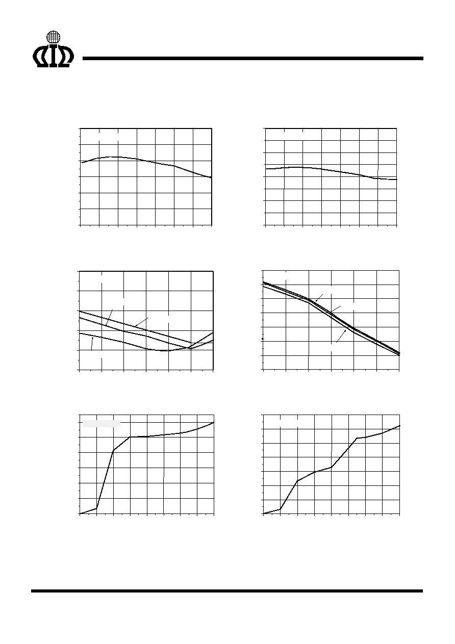
TYPICAL PERFORMANCE CHARACTERISTICS
-40
-20
0
20
40
60
80
100
2.46
2.47
2.48
2.49
2.50
2.51
2.52
AIC1722A-25
V
OUT
vs. Temperature
V
OUT
(V)
Temperature (
∞C)
-40
-20
0
20
40
60
80
100
5.10
5.15
5.20
5.25
5.30
V
OUT
(V)
Temperature (
∞C)
V
OUT
vs. Temperature
AIC1722A-52
G
r
ound C
u
rre
nt (uA)
-40
-20
0
20
40
60
80
45
50
55
60
65
70
AIC1722A-25
Temperature (
∞C)
Ground Current vs. Temperature
I
LOAD
=100mA
I
LOAD
=300mA
I
LOAD
=0mA
Temperature (
∞C)
-40
-20
0
20
40
60
80
46
48
50
52
54
56
58
60
I
LOAD
=0mA
Ground Current vs. Temperature
G
r
ound Curre
nt (uA)
AIC1722A-52
I
LOAD
=100mA
I
LOAD
=300mA
0
1
2
3
4
5
6
7
8
0
10
20
30
40
50
60 AIC1722A - 25
G
r
ound
C
u
rre
nt (uA)
V
IN
(V)
Ground Current vs. V
IN
0
1
2
3
4
5
6
7
8
0
10
20
30
40
50
60
70
AIC1722A-52
Ground Current vs. V
IN
G
r
ound C
u
rre
nt (uA)
V
IN
(V)
5
AIC1722A
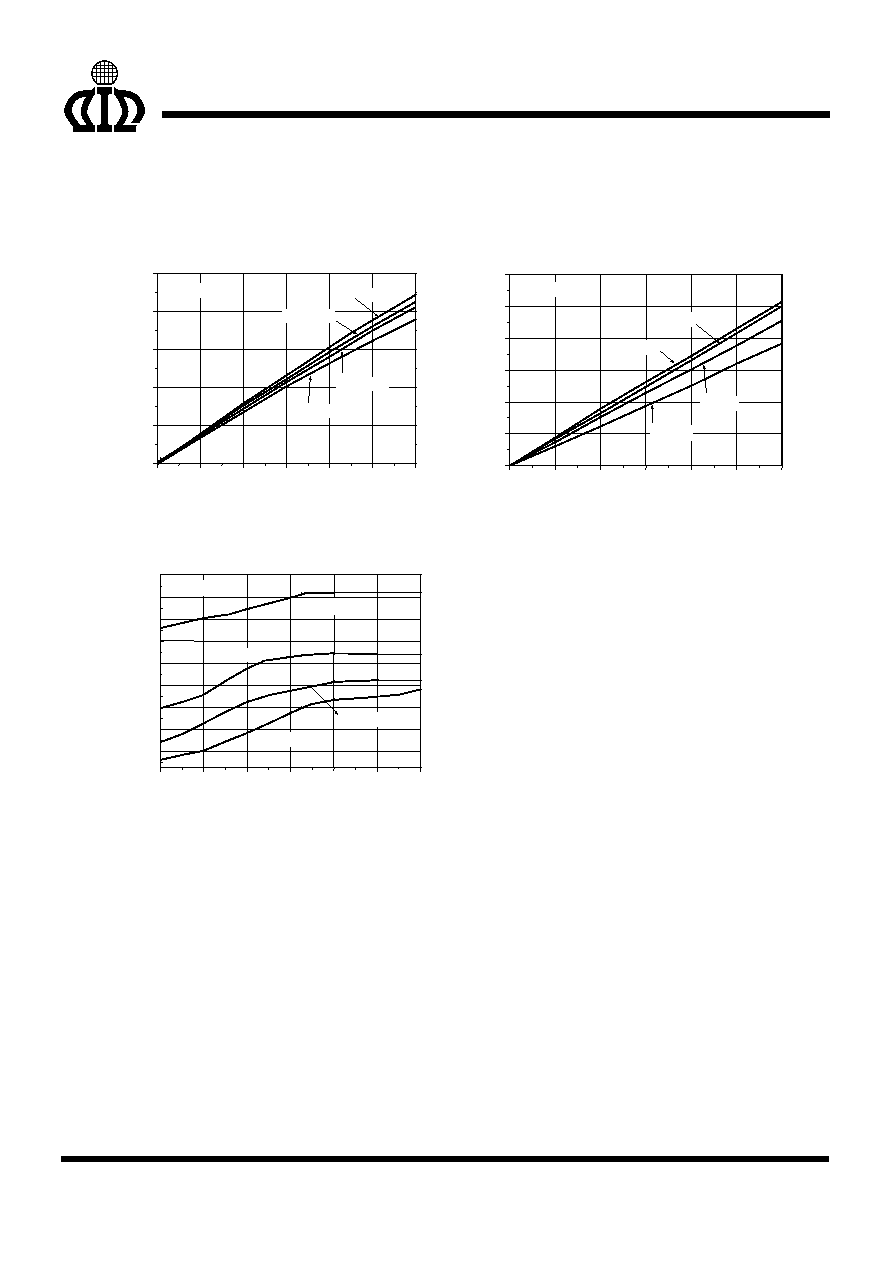
TYPICAL PERFORMANCE CHARACTERISTICS
(Continued)
0
50
100
150
200
250
300
0
100
200
300
400
500
T=80
∞C
AIC1722A-25
V
DR
OP
(m
V)
I
LOAD
(mA)
V
DROP
vs. I
LOAD
T=50
∞C
T=20
∞C
T=-40
∞C
AIC1722A-52
T=80
∞C
T=50
∞C
T=20
∞C
T=-40
∞C
0
50
100
150
200
250
300
0
50
100
150
200
250
300
V
DROP
vs. I
LOAD
V
DRO
P
(mV)
I
LOAD
(mA)
-40
-20
0
20
40
60
80
460
470
480
490
500
510
520
530
540
V
IN
=7V
V
IN
=6V
V
IN
=5V
AIC1722A
Currnet L
i
m
i
t (m
A)
Temperature (
∞C)
Current Limit vs. Temperature
V
IN
=4V
6
AIC1722A
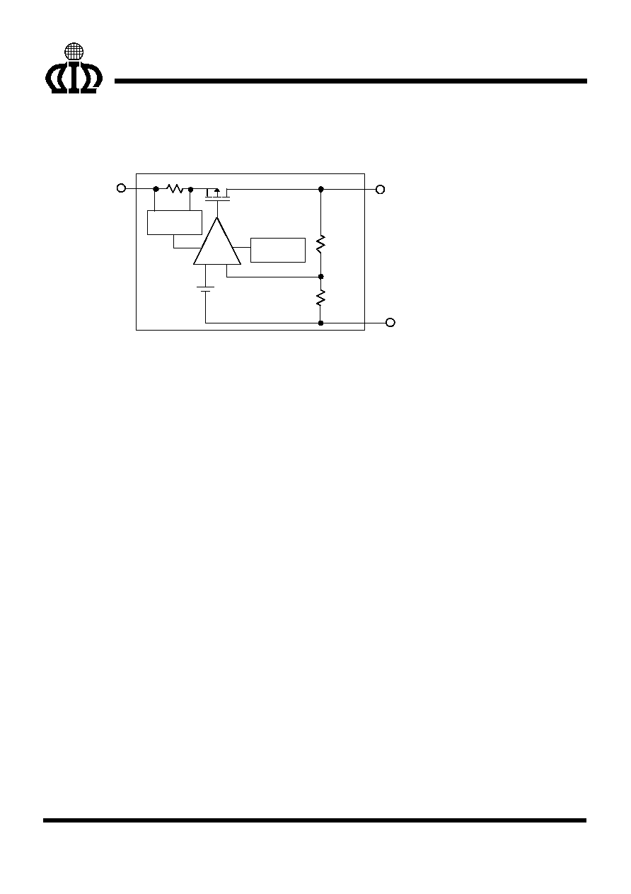
BLOCK DIAGRAM
1.235V
Reference
GND
VOUT
VIN
ERROR
AMP
+
-
THERMAL
SHUTDOWN
-
+
CURRENT
LIMITING
PIN DESCRIPTIONS
VOUT PIN - Output pin.
GND PIN - Power GND.
VIN PIN - Power Supply Input.
7
AIC1722A
PHYSICAL DIMENSIONS
(unit: mm)
SOT-23 (CU) (PU)
SYMBOL MIN MAX
A 0.95
1.45
A1 0.05
0.15
A2 0.90
1.30
b 0.30
0.50
c 0.08
0.22
D 2.80
3.00
E 2.60
3.00
E1 1.50
1.70
e 0.95
BSC
e1 1.90
BSC
L 0.30
0.60
L1 0.60
REF
E
D
E1
e1
e
A1
A
A2
b
0.25
L1
L
c
0∞
8∞
SOT-89 (CXX) (PXX)
SYMBOL MIN
MAX
A 1.40 1.60
B 0.44 0.56
B1 0.36 0.48
C 0.35 0.44
D 4.40 4.60
D1 1.50 1.83
E 2.29 2.60
e 1.50
BSC
e1 3.00
BSC
H 3.94 4.25
B1
e
H
e1
D
D1
A
C
L
E
B
L 0.89 1.20
8

AIC1722A
9
TO-92 (CZ)(PZ)
SYMBOL MIN MAX
A 4.32
5.33
b 0.36
0.47
D 4.45
5.20
E 3.18
4.19
e 2.42
2.66
e1 1.15 1.39
j 3.43 -
L 12.70 -
S 2.03
2.66
A
e1
e
L
D
S
E
j
b
Note:
Information provided by AIC is believed to be accurate and reliable. However, we cannot assume responsibility for use of any
circuitry other than circuitry entirely embodied in an AIC product; nor for any infringement of patents or other rights of third par-
ties that may result from its use. We reserve the right to change the circuitry and specifications without notice.
Life Support Policy: AIC does not authorize any AIC product for use in life support devices and/or systems. Life support devices
or systems are devices or systems which, (I) are intended for surgical implant into the body or (ii) support or sustain life, and
whose failure to perform, when properly used in accordance with instructions for use provided in the labeling, can be reasonably
expected to result in a significant injury to the user.