AIC1739
300mA Low Dropout Linear Regulator
Analog Integrations Corporation
4F, 9 Industry E. 9th Rd, Science-Based Industrial Park, Hsinchu, Taiwan
DS-1739-01 012102
TEL: 886-3-5772500
FAX: 886-3-5772510
www.analog.com.tw
1
n
FEATURES
l
Low Dropout Voltage of 180mV at 100mA
Output Current (3.0V Output Version).
l
Guaranteed 300mA Output Current.
l
Internal 1.3
P-MOSFET Draws no Base
Current.
l
Low Ground Current at 55
�
A.
l
2% Accuracy Output Voltage of 1.8V/ 2.0V/
2.5V/ 2.7V/ 3.0V.
l
Input Voltage Range up to 12V.
l
Needs only 1
�
F for Stability.
l
Current and Thermal Limiting.
n
APPLICATIONS
l
Voltage Regulator for CD-ROM Drivers.
l
Voltage Regulator for LAN Cards.
l
Voltage Regulator for Microprocessor.
l
Wireless Communication Systems.
l
Battery Powered Systems.
n
DESCRIPTION
The AIC1739 is a 3-pin low dropout linear
regulator. The superior characteristics of the
AIC1739 include zero base current loss, very
low dropout voltage, and 2% accuracy output
voltage. Typical ground current remains
approximately 55
�
A, from no load to
maximum loading conditions. Dropout voltage
is exceptionally low. Output current limiting
and thermal limiting are built in to provide
maximal protection to the AIC1739 against
fault conditions.
The AIC1739 comes in the popular 3-pin
SOT-89 and TO-92 packages.
n
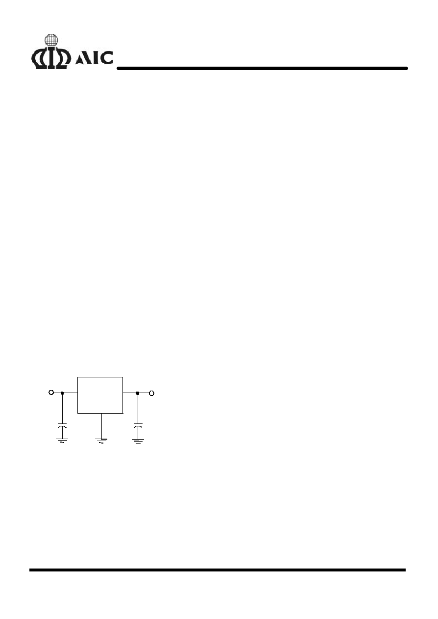
TYPICAL APPLICATION CIRCUIT
+
+
AIC1739
10
�
F
C
OUT
V
OUT
VOUT
GND
VIN
1
�
F
C
IN
V
IN
Low Dropout Linear Regulator
AIC1739
2
n
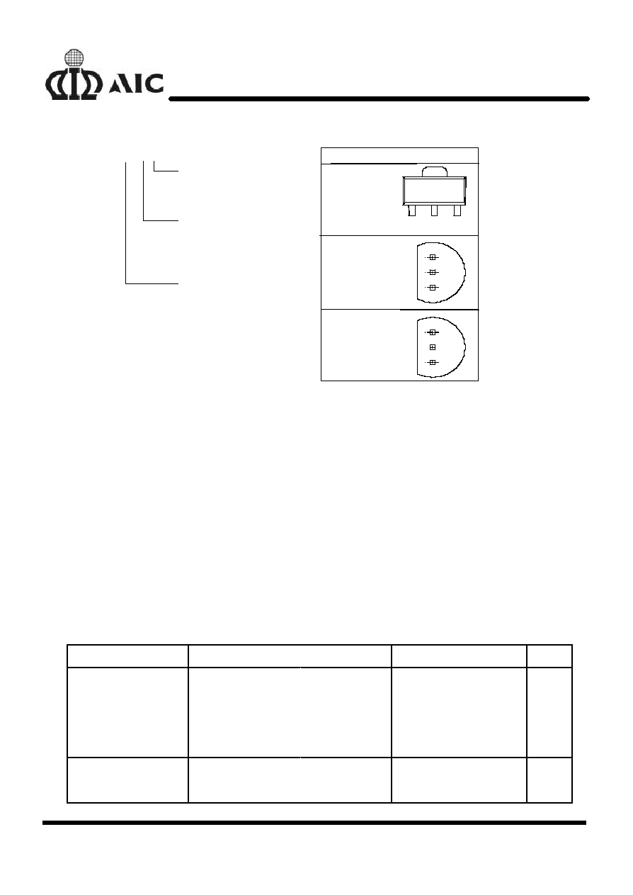
ORDERING INFORMATION
PIN CONFIGURATION
SOT-89
FRONT VIEW
1. VOUT
2. GND
3. VIN
1
2
3
1
2
3
1
2
3
TO-92
TOP VIEW
1. GND
2. VIN
3. VOUT
TO-92
TOP VIEW
1. VIN
2. GND
3. VOUT
AIC1739-XXCXXX
PACKING TYPE
TR: TAPE & REEL
BG: BAG
PACKAGING TYPE
X: SOT89
ZT: TO92
ZL: TO92
OUTPUT VOLTAGE
18: 1.8V
20: 2.0V
25: 2.5V
27: 2.7V
30: 3.0V
Example: AIC1739-18CXTR
�
1.8V Version, in SOT-89 Package
& Tape & Reel Packing Type
n
ABSOLUTE MAXIMUM RATINGS
Input Supply Voltage ...................................................... ... ... ... ..... ... .................. -0.3~12V
Operating Junction Temperature Range
........ ... ... ........... ... ... ... ................ -40
�
C~ 85
�
C
Storage Temperature Range ....................... ... ......................... ... ... .............. -65
�
C~150
�
C
Power Dissipation
SOT-89 Package ....... ...... ................. 0.5W
TO-92 Package ........ ... ... ... ............. 0.5W
n
TEST CIRCUIT
Refer to the TYPICAL APPLICATION CIRCUIT
n
ELECTRICAL CHARACTERISTICS
(Ta=25
�
C, C
IN
=1
�
F, C
OUT
=10
�
F, unless
otherwise specified.)
PARAMETER
TEST CONDITIONS
MIN.
TYP.
MAX.
UNIT
Output Voltage
No Load
AIC1739-30
AIC1739-27
AIC1739-25
AIC1739-20
AIC1739-18
V
IN
=4.0~12V
V
IN
=4.0~12V
V
IN
=4.0~12V
V
IN
=4.0~12V
V
IN
=4.0~12V
2.940
2.646
2.450
1.960
1.764
3.000
2.700
2.500
2.000
1.800
3.060
2.754
2.550
2.040
1.836
V
Output Voltage
Temperature
Coefficiency
(Note 1)
50
150
PPM/
�
C
AIC1739
3
n
ELECTRICAL CHARACTERISTICS
(Continued)
PARAMETER
TEST CONDITIONS
MIN.
TYP.
MAX.
UNIT
Line Regulation
I
L
=1mA
V
IN
=4.0~12V
3
10
mV
Load Regulation
(Note 2)
V
IN
=5V, I
L
=0.1~300mA
7
25
mV
Current Limit
(Note 3)
V
IN
=5V, V
OUT
=0V
320
440
mA
Dropout Voltage
(Note 4)
AIC1739s
AIC1739-30
AIC1739-27
AIC1739-25
AIC1739-20
AIC1739-18
I
L
=0.1mA
I
L
=300mA
I
L
=300mA
I
L
=300mA
I
L
=300mA
I
L
=300mA
0.2
540
570
610
820
920
10
640
670
710
970
1070
mV
Ground Current
I
O
=0.1mA~I
MAX
V
IN
=4~12V
55
80
�
A
Note 1:
Guaranteed by design.
Note 2:
Regulation is measured at constant junction temperature, using pulse testing with a low ON time.
Note 3:
Current limit is measured by pulsing a short time.
Note 4:
Dropout voltage is defined as the input to output differential at which the output voltage drops
100mV below the value measured with a 1V differential.
n
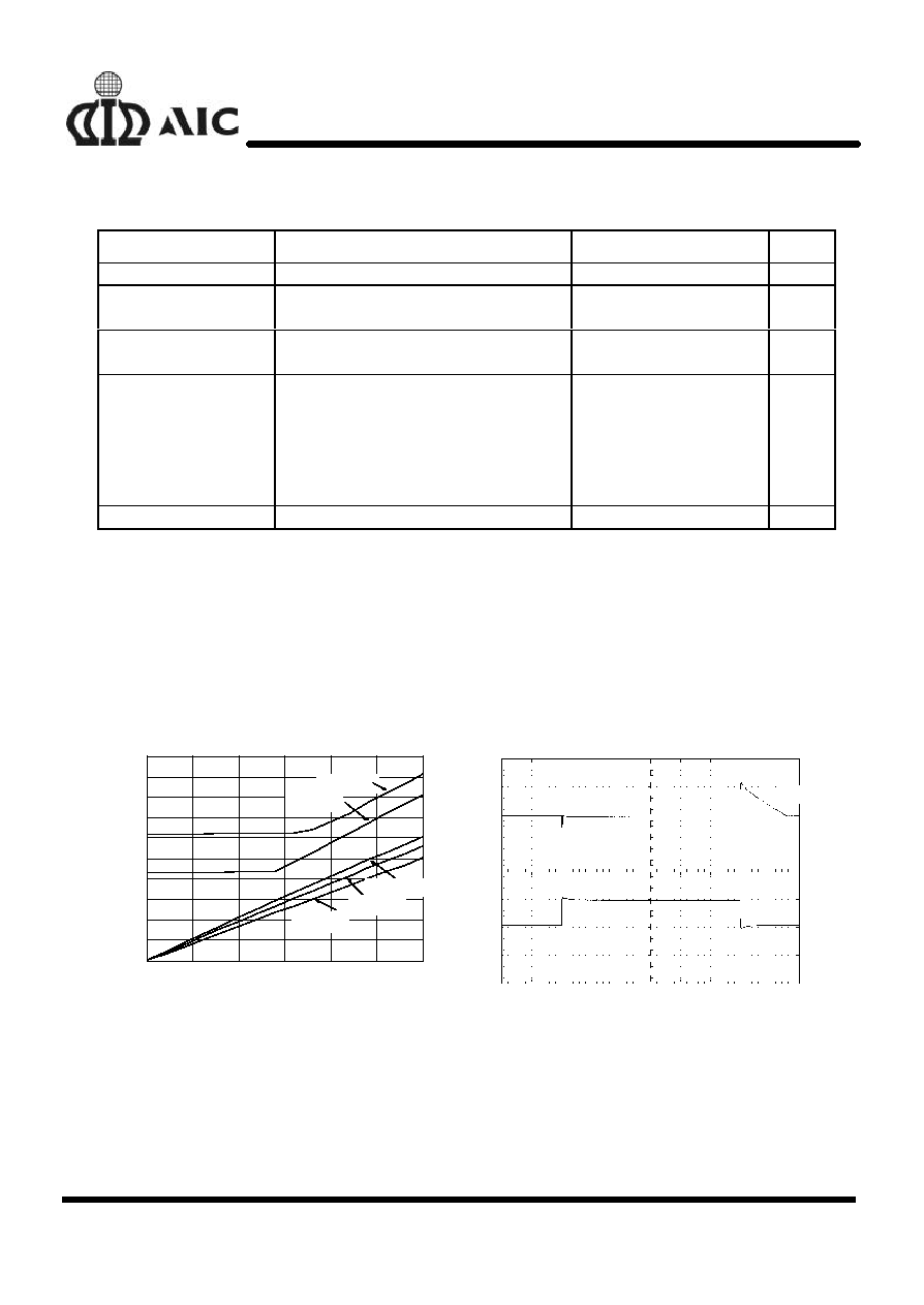
TYPICAL PERFORMANCE CHARACTERISTICS
Dropout Voltage (mV)
Load Current (mA)
0
50
100
150
200
250
300
0
100
200
300
400
500
600
700
800
900
1000
Dropout Voltage vs Load Current
V
OUT
=2.7V
V
OUT
=3.0V
V
OUT
=2.0V
V
OUT
=1.8V
V
OUT
=2.5V
V
OUT
V
OUT
=3.0V
100mV/DIV
I
OUT
I
OUT
=0.1mA
I
OUT
=150mA
Time (0.5mS/DIV)
C
OUT
=1
�
F
Load Transient Response
AIC1739
4
n
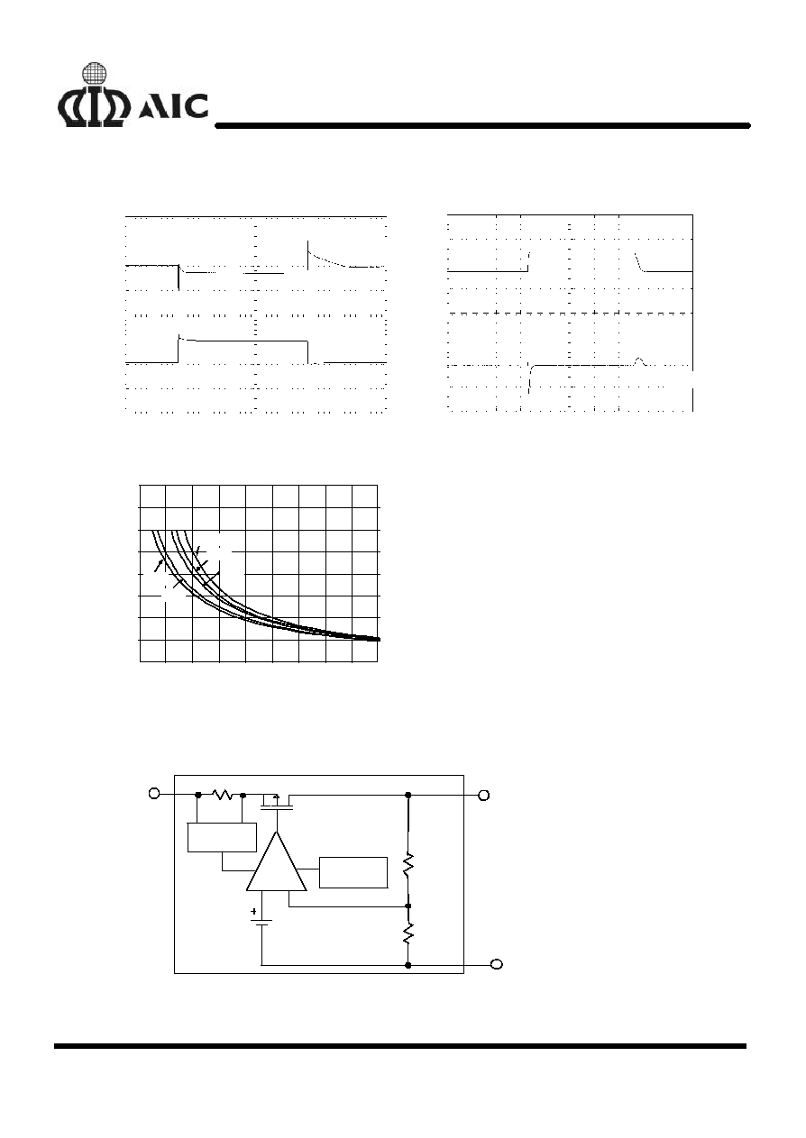
TYPICAL PERFORMANCE CHARACTERISTICS
(Continued)
V
OUT
V
OUT
=3.0V
20mV/DIV
I
OUT
I
OUT
=0.1mA
I
OUT
=150mA
Time (0.5mS/DIV)
C
OUT
=10
�
F
Load Transient Response
V
IN
V
IN
=4.0
V
20mV/DIV
V
OUT
V
OUT
=3.0V
Time (1mS/DIV)
V
IN
=6V
Line Transient Response
C
OUT
=1
�
F
I
L
=1mA
Dropout Voltage (mV)
Input Voltage (V)
Recommended max. Output Current vs. Input voltage
3
4
5
6
7
8
9
10
11
12
0
5 0
100
150
200
250
300
350
400
2.0V
2.5V
3.0V
2.7V
1.8V
n
BLOCK DIAGRAM
1.235V
Reference
GND
VOUT
VIN
ERROR
AMP
-
THERMAL
SHUTDOWN
-
+
CURRENT
LIMITING
AIC1739
5
n
PIN DESCRIPTION
VOUT PIN - Output pin.
GND PIN - Power GND.
VIN PIN
- Power Supply Input.
n
APPLICATION INFORMATIONS
A 1
�
F (or greater) capacitor is required between
the AIC1739 output and ground for stability.
Without this capacitor the part will oscillate. Even
though most types of capacitor may work, the
equivalent series resistance (ESR) should be held
to 5
or less if Aluminum electrolytic type is used.
Many Aluminum electrolytics have electrolytes
that freeze at about -30
�
C, so solid tantalums are
recommended for operation below -25
�
C. The
value of this capacitor may be increased without
limit.
A 0.1
�
F capacitor (or greater) should be placed
from the AIC1739 input to ground if the lead
inductance between the input and power source
exceeds 500nH (approximately 10 inches of trace).
n
PHYSICAL DIMENSIONS
l
SOT-89 (unit: mm)
SYMBOL
MIN
MAX
A
1.40
1.60
B
0.36
0.48
C
0.35
0.44
D
4.40
4.60
D1
1.62
1.83
E
2.29
2.60
e
1.50 (TYP.)
e1
3.00 (TYP.)
H
3.94
4.25
B
e
H
e1
D
D1
A
C
L
E
L
0.89
1.20
SOT-89 MARKING
Part No.
Marking
AIC1739-18
AY18
AIC1739-20
AY20
AIC1739-25
AY25
AIC1739-27
AY27
AIC1739-30
AY30
AIC1739
6
l
TO-92 (unit: mm)
SYMBOL
MIN
MAX
A
4.32
5.33
C
0.38 (TYP.)
D
4.40
5.20
E
3.17
4.20
e1
1.27 (TYP.)
A
L
e1
D
C
E
L
12.7
-