AIC1742
Low Noise, Low Quiescent Current,
150mA Linear Regulator with Noise Bypass
Analog Integrations Corporation
Si-Soft Research Center
DS-1742P-02 010405
3A1, No.1, Li-Hsin Rd. I , Science Park , Hsinchu 300, Taiwan , R.O.C.
FEATURES
Very Low Noise, 25V
RMS
@ f=10~100kHz.
Very Low Quiescent Current, 35A.
Very Low Dropout Voltage, 90mV @ 50mA.
Active Low Shutdown Control.
Short Circuit and Thermal Protection.
1.5V, 1.8V, 2.0V, 2.5V, 2.8V, 2.85V, 2.9V, 3.0V,
3.3V Output Voltage.
Available in
�2% Output Tolerance.
Low Profile Package: SOT-23-5
APPLICATIONS
Cellular Telephones.
Pagers.
Personal Communication Equipment.
Cordless Telephones.
Portable Instrumentation.
Portable Consumer Equipment.
Radio Control Systems.
Low Voltage Systems.
Battery Powered Systems
DESCRIPTION
AIC1742 is a low noise, low dropout linear
regulator, and is housed in a small SOT-23-5
package. The device is in the "ON" state when
the SHDN pin is set to logic high level. A low
dropout voltage of 90mV at 50mA load current
is performed. It offers high precision output
voltage of
�2%. The quality of low quiescent
current and low dropout voltage makes this
device ideal for battery power applications.
The internal reverse bias protection eliminates
the requirement for a reverse voltage
protection diode. The high ripple rejection and
low noise of AIC1742 provide enhanced
performance for critical applications. The
noise bypass pin can be connected an
external capacitor to reduce the output noise
level.
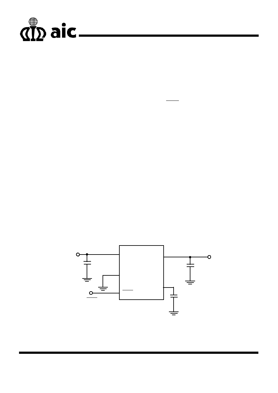
TYPICAL APPLICATION CIRCUIT
C
IN
1
�F
V
IN
BP
VOUT
SHDN
GND
VIN
AIC1742
C
OUT
2.2
�F
C
BP
0.01
�F
V
SHDN
V
OUT
* C
IN
: TAIYO YUDEN, CEJMK107BJ105MA-T
*C
OUT
: TAIYO YUDEN, CEJMK107BJ225M-T
Low Noise Low Dropout Linear Regulator
TEL: 886-3-5772500
FAX: 886-3-5772510
www.analog.com.tw
1
AIC1742
ORDERING INFORMATION
PIN CONFIGURATION
Example: AIC1742-15ACVTR
1.5V Version, in SOT-23-5 Package & Tape &
Reel Packing Type
AIC1742-15APVTR
1.5V Version, in SOT-23-5 Lead Free
Package & Tape & Reel Packing Type
AIC1742-XXX XXX XX
PACKING TYPE
TR: TAPE & REEL
BG: BAG
C: COMMERCIAL
ACV: SOT-23-5
BCV: SOT-23-5
P: LEAD FREE COMMERCIAL
APV: SOT-23-5
BPV: SOT-23-5
OUTPUT VOLTAGE
15:
1.5V
18
: 1.8V
20: 2.0V
25: 2.5V
28: 2.8V
285: 2.85V
29: 2.9V
30: 3.0V
33: 3.3V
(Of a unit of 0.1V within the voltage
range from 1.5V to 3.3V, additional
voltage versions for this product line
may be available on demand with prior
consultation with AIC.)
3
2
1
4
5
SOT-23-5
FRONT VIEW
(AXV)
1. VIN
2. GND
3. SHDN
4. BP
5. VOUT
(BXV)
1. VOUT
2. GND
3. VIN
4. SHDN
5. BP
2
AIC1742
� SOT-23-5 Marking
Part No.
ACV
APV
Part No.
BCV
BPV
AIC1742-15AXV ER15 ER15P
AIC1742-15BXV ES15 ES15P
AIC1742-18AXV ER18 ER18P
AIC1742-18BXV ES18 ES18P
AIC1742-20AXV ER20 ER20P
AIC1742-20BXV ES20 ES20P
AIC1742-25AXV ER25 ER25P
AIC1742-25BXV ES25 ES25P
AIC1742-28AXV ER28 ER28P
AIC1742-28BXV ES28 ES28P
AIC1742-285AXV ER2J ER2JP AIC1742-285BXV ES2J ES2JP
AIC1742-29AXV ER29 ER29P
AIC1742-29BXV ES29 ES29P
AIC1742-30AXV ER30 ER30P
AIC1742-30BXV ES30 ES30P
AIC1742-33AXV ER33 ER33P
AIC1742-33BXV ES33 ES33P
ABSOLUTE MAXIMUM RATINGS
Supply Voltage
9V
Shutdown Terminal Voltage
.9V
Power Dissipation
500mW
Operating Temperature Range
-40�C~85�C
Maximum Junction Temperature
125
�C
Storage Temperature Range
-65�C~150�C
Lead Temperature (Soldering, 10 sec)
260
�C
Thermal Resistance Junction to Case
130�C/W
Thermal Resistance Junction to Ambient
220�C/W
(Assume no ambient airflow, no heatsink)
Absolute Maximum Ratings are those values beyond which the life of a device may be impaired.
TEST CIRCUIT
Refer to TYPICAL APPLICATION CIRCUIT
3
AIC1742
ELECTRICAL CHARACTERISTICS
(T
J
=25
�C, unless otherwise specified) (Note1)
PARAMETER TEST
CONDITIONS
SYMBOL
MIN.
TYP.
MAX.
UNIT
Quiescent Current
V
IN
= V
OUT
+ 1V,
V
SHDN
=1.6V, I
OUT
= 0mA
I
Q
35 45
�A
Standby Current
V
IN
= V
OUT
+ 1V to 8V,
V
SHDN
=0.6V, Output OFF
I
STBY
0.1
�A
GND Pin Current
I
OUT
= 50mA
I
GND
2.5
3.5
mA
Continuous Output Current
V
IN
= V
OUT
+ 1V to 8V
I
OUT
150
mA
Output Current Limit
V
IN
= V
OUT
+ 1V, V
OUT
= 0V
I
IL
150 250 mA
Output Voltage Tolerance
V
IN
= V
OUT
+ 1V, no load
V
OUT
-2 2 %
Temperature Coefficient
T
C
50
150
ppm/�C
Line Regulation
V
IN
= V
OUT
TYP
+ 1V to 8V
V
LIR
2 5
mV
Load Regulation
V
IN
= 5V,
I
OUT
= 0.1~150mA
V
LOR
0.005
0.01
%/mA
I
OUT
= 50 mA
90
160
I
OUT
= 100 mA
140
230
I
OUT
= 150 mA
Vout
2.5V
200
350
Dropout Voltage
I
OUT
= 150 mA Vout<2.5V
V
DROP
500
800
mV
Noise Bypass Terminal
Voltage
V
REF
1.25 V
Ripple Rejection
f=1KHz, Ripple=0.5V
P-P
,
C
BP
= 0.1
�F
RR 65 dB
Output Noise
C
BP
= 0.1
�F, f = 10~100KHz
n
25
�Vrms
SHUTDOWN TERMINAL SPECIFICATIONS
Shutdown Pin Current
V
SHDN
=1.6V I
SHDN
2
�A
Shutdown Pin Voltage (ON) Output ON
V
SHDN
ON
1.6 V
Shutdown Pin Voltage (OFF) Output OFF
V
SHDN
OFF
0.6
V
Shutdown Exit Delay Time
C
BP
= 0.1
�F, C
OUT
= 1
�F,
I
OUT
=30mA
t
300
�S
Note 1: Specifications are production tested at TA=25
�C. Specifications over the -40�C to 85�C operating
temperature range are assured by design, characterization and correlation with Statistical Quality
Controls (SQC).
Note 2: The dropout voltage is defined as V
IN
� V
OUT
when V
OUT
is 1% below the value of V
OUT
for
V
IN
= V
OUT
+ 0.5V. (Only applicable for V
OUT
= 2.5V ~ 5V)
4
AIC1742
TYPICAL PERFORMANCE CHARACTERISTICS
2
3
4
5
6
7
8
9
10
0
10
20
30
40
50
60
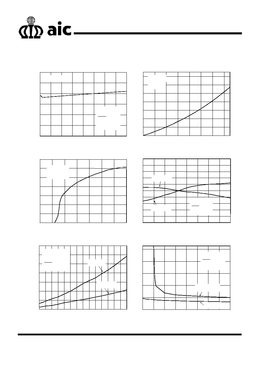
Fig. 1 Quiescent Current
Quiescent Current
(
�
A)
Input Voltage (V)
AIC1742
T
A
=25
�C
V
SHDN
=1.6V
I
OUT
=0mA
Fig. 2 Ground Current
Gr
o
u
n
d
Curren
t
(mA
)
0
20
40
60
80
100
120
140
0
2
4
6
8
10
12
14
Output Current (mA)
T
A
=25
�C
AIC1742
Fig. 3
Short-Circuit Current
Sho
r
t-Ci
rcui
t Cu
rrent
(
mA
)
0
1
2
3
4
5
6
7
0
50
100
150
200
250
300
350
Input Voltage (V)
AIC1742
T=25
�C
Fig. 4 Output Voltage
Ou
tp
ut
V
o
l
t
ag
e De
vi
at
i
o
n
(%)
-40
-20
0
20
40
60
80
100
120
-1.0
-0.8
-0.6
-0.4
-0.2
0.0
0.2
0.4
0.6
0.8
1.0
AIC1742-33
AIC1742-15
Temperature (
�C)
V
IN
=5V
V
SHDN
=1.6V
I
OUT
=0mA
Fig. 5 Load Regulation
Lo
ad
Reg
u
l
a
t
i
on
(mV
)
10
20
30
40
50
60
70
80
90
100
110
120 130 140 150
0
5
10
15
20
25
30
35
AIC1742-33
AIC1742-15
Output Current (mA)
AIC1742
V
IN
=5V
V
SHDN
=1.6V
T
A
=25
�C
Lo
ad
Reg
u
l
a
t
i
on
(mV
)
2.0
2.5
3.0
3.5
4.0
4.5
5.0
5.5
6.0
0
10
20
30
40
50
I
OUT
=100mA
I
OUT
=150mA
Fig. 6 Load Regulation
Input Voltage (V)
AIC1742-15
V
SHDN
=1.6V
T
A
=25
�C
5
AIC1742
TYPICAL PERFORMANCE CHARACTERISTICS
(Continued)
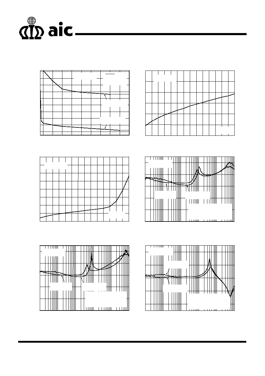
Fig. 7 Load Regulation
Lo
ad
Reg
u
l
a
ti
o
n
(mV)
3.5
4.0
4.5
5.0
5.5
6.0
6.5
7.0
7.5
8.0
16
18
20
22
24
26
28
30
32
34
I
OUT
=100mA
Input Voltage (V)
V
SHDN
=1.6V
T
A
=25
�C
I
OUT
=150mA
AIC1742-33
Drop
ou
t V
o
lt
ag
e (mV)
Fig. 8 Dropout Voltage
10
20
30
40
50
60
70
80
90
100
110 120
130 140 150
0
50
100
150
200
250
300
Output Current (mA)
T
A
=25
�C
AIC1742-25
Drop
ou
t V
o
lt
ag
e (mV)
Fig. 9 Dropout Voltage
Output Current (mA)
10
20
30
40
50
60
70
80
90
100
110
120 130 140 150
0
100
200
300
400
500
600
700
800
T
A
=25
�C
AIC1742-20
Ri
pp
le
R
e
j
e
c
t
io
n
(
d
B)
Fig. 10 Input Ripple Rejection
10
10
2
10
3
10
4
10
5
10
6
0
20
40
60
80
100
C
OUT
=2.2
�F Ceramic
I
OUT
=0mA
C
BP
=0.1
�F
Frequency (Hz)
C
BP
=0.01
�F
AIC1742-20
Ri
pp
le
R
e
j
e
c
t
io
n
(
d
B)
Fig. 11 Input Ripple Rejection
0
20
40
60
80
100
Frequency (Hz)
C
OUT
=2.2
�F Ceramic
I
OUT
=0mA
C
BP
=0.1
�F
C
BP
=0.01
�F
AIC1742-30
10
10
2
10
3
10
4
10
5
10
6
Ri
p
p
l
e
Rej
e
ct
io
n (dB
)
Fig. 12 Input Ripple Rejection
Frequency (Hz)
0
20
40
60
80
100
C
OUT
=2.2
�F Ceramic
I
OUT
=100mA
C
BP
=0.01
�F
C
BP
=0.1
�F
AIC1742-20
10
10
2
10
3
10
4
10
5
10
6
6
AIC1742
TYPICAL PERFORMANCE CHARACTERISTICS
(Continued)
Ri
p
p
l
e
Rej
e
ct
io
n (dB
)
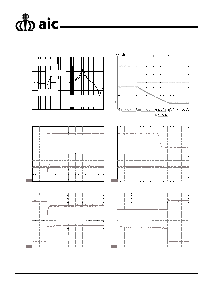
Fig. 13 Input Ripple Rejection
Frequency (Hz)
10
10
2
10
3
10
4
10
5
10
6
0
20
40
60
80
100
C
OUT
=2.2
�F Ceramic
I
OUT
=100mA
C
BP
=0.01
�F
C
BP
=0.1
�F
AIC1742-30
Fig. 14 Shutdown Delay
V
SHDN
, 2V/Div
V
OUT
, 1V/Div
1
2
1) Ch 1: 500 mVolt 25 us
2) Ch 2: 20 mVolt 25 us
Fig. 15 Line Transient Response
Vout, 20mV/Div
Vin, 500mV/Div
V
IN
=3.5~4.5V V
OUT
=2.5V
C
OUT
=2.2
�F Ceramic
I
OUT
=60mA
1
2
1) Ch 1: 500 mVolt 100 us
2) Ch 2: 20 mVolt 100 us
Fig. 16 Line Transient Response
Vout, 20mV/Div
Vin, 500mV/Div
V
IN
=4.5~3.5V V
OUT
=2.5V
C
OUT
=2.2
�F Ceramic
I
OUT
=60mA
1
2 >
1) Ch 1: 20 mVolt 10 us
2) Ch 2: 10 mVolt 10 us
Fig. 17 Transient Response 2
V
IN
=5V V
OUT
=2.5V
C
OUT
=2.2
�F Ceramic
I
OUT
=0~100mA
Vout, 20mV/Div
Iout, 50mA/Div
1
2 >
1) Ch 1: 20 mVolt 10 us
2) Ch 2: 10 mVolt 10 us
Fig. 18 Load Transient Response
V
IN
=5V V
OUT
=2.5V
C
OUT
=2.2
�F Ceramic
Iout=0~100mA
CH1:20mV/Div
Iout, 50mA/Div
7
AIC1742
TYPICAL PERFORMANCE CHARACTERISTICS
(Continued)
Ou
tp
u
t
No
i
s
e
(
�
V)
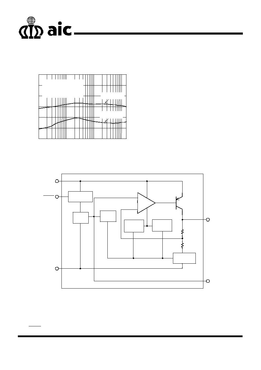
Fig. 19 Output Noise RMS
Output Current (mA)
0.1
1
10
100
0
10
20
30
40
50
60
AIC1742-15
AIC1742-33
C
OUT
=4.7
�F Ceramic
C
NB
=0.01
�F
f=10Hz to 100KHz
BLOCK DIAGRAM
Amp
Error
VOUT
BP
Circuit
Bias
Circuit
Disconnect
VIN
SHDN
Circuit
Control
1.25V
REF
Limit
Current
Thermal
Shutdown
-
+
GND
PIN DESCRIPTIONS
VIN PIN - Power supply input pin. Bypass
with a 1
�F capacitor to GND.
BP
PIN - Noise bypass pin. An external
bypass capacitor connecting to BP
pin to reduce noises at the output.
GND PIN - Ground pin.
SHDN
PIN - Active-Low shutdown input pin.
VOUT PIN - Output pin. Sources up to 150 mA.
8
AIC1742
9
DETAILED DESCRIPTION OF TECHNICAL TERMS
DROPOUT VOLTAGE (V
DROP
)
The dropout voltage is defined as the difference
between the input voltage and output voltage at
which the output voltage drops 100mV. Below
this value, the output voltage will fall as the input
voltage reduces. It depends on the load current
and junction temperature.
LINE REGULATION
Line regulation is the ability of the regulator to
maintain a constant output voltage as the input
voltage changes. The line regulation is specified
as the input voltage changes from V
IN
= V
OUT
+
1V to V
IN
= 8V and I
OUT
= 1mA.
LOAD REGULATION
Load regulation is the ability of the regulator to
maintain a constant output voltage as the load
current changes.
A pulsed measurement with an
input voltage set to V
IN
= V
OUT
+ V
DROP
can
minimize temperature effects.
The load
regulation is specified by the output current
ranging from 0.1mA to 150mA.
QUIESCENT CURRENT (I
Q
)
Quiescent current is the current flowing through
ground pin with no output load.
GROUND CURRENT (I
GND
)
Ground current is the current flowing through the
ground pin with output load.
STANDBY CURRENT (I
STBY
)
Standby current is the current flowing into the
regulator when the output is shutdown by setting
V
SHDN
at 0V and V
IN
at 8 V.
CURRENT LIMIT (I
IL
)
Current limiting of AIC1742 monitors and controls
the maximum output current, in case of a shorted
output. It protects device from the damage
resulting from any unexpected current.
RIPPLE REJECTION (RR)
Ripple rejection is the ability of the regulator to
reduce voltage ripple, which comes from input, at
output terminal. It is specified with a signal of
0.5V
P-P
at 1KHz frequency applying to input,
output capacitor at 2.2
�F as well as a noise
bypass of 0.1
�F. Ripple rejection, expressed in
dB, is the ratio of output ripple to input.
THERMAL PROTECTION
Thermal sensor protects device when the
junction temperature exceeds T
J
= +155�C. It
signals shutdown logic, turning off pass transistor
and allowing IC to cool down. After the IC's
junction temperature cools by 15�C, the thermal
sensor will turn the pass transistor back on.
Thermal protection is designed to protect the
device in the event of fault conditions. For a
continuous operation, do not exceed the absolute
maximum junction-temperature rating of T
J
=
150�C, or damage may occur to the device.

AIC1742
APPLICATION INFORMATION
INPUT-OUTPUT CAPACITORS
Linear regulators require input and output
capacitors to maintain stability.
Input capacitor
at 1
�F with 1uF aluminum electrolytic or 2.2�F
ceramic output capacitor is recommended. And
it should be selected within the Equivalent
Series Resistance (ESR) range as shown in
the figure 20,21. ESR of ceramic capacitor is
lower and its electrical characteristics
(capacitance and ESR) vary widely over
temperature. In general, tantalum or electric
output capacitor is suggested for heavy load.
Normally, the output capacitor should be 1
�F
(aluminum electrolytic) at least and rates for
operating temperature range. Note that it's
important to check selected manufactures
electrical characteristics (capacitance and ESR)
over temperature.
NOISE BYPASS CAPACITOR
0.01
�F bypass capacitor at BP pin reduces
output voltage noise. And the BP pin has to
connect a capacitor to GND.
POWER DISSIPATION
The maximum power dissipation of AIC1742
depends on the thermal resistance of its case
and circuit board, the temperature difference
between the die junction and ambient air, and
the rate of airflow. The rate of temperature rise
is greatly affected by the mounting pad
configuration on the PCB, the board material,
and the ambient temperature. When the IC
mounting with good thermal conductivity is
used, the junction temperature will be low even
when large power dissipation applies.
The power dissipation across the device is
P = I
OUT
(V
IN
-V
OUT
).
The maximum power dissipation is:
)
R
(R
)
T
(T
P
BA
JB
A
J
MAX
+
-
=
Where T
J
-T
A
is the temperature difference
between the die junction and the surrounding
air, R
JB
is the thermal resistance of the
package, and R
BA
is the thermal resistance
through the PCB, copper traces, and other
materials to the surrounding air.
As a general rule, the lower temperature is, the
better reliability of the device is. So the PCB
mounting pad should provide maximum
thermal conductivity to maintain low device
temperature.
GND pin performs a dual function of providing
an electrical connection to ground and
channeling heat away. Therefore, connecting
the GND pin to ground with a large pad or
ground plane would increase the power
dissipation and reduce the device temperature.
10

AIC1742
11
S
e
ria
l
Re
s
i
sto
r
(
)
F
C
OU
T
ES
R
(
)
ent
0
20
40
60
80
100
120
140
0.01
0.1
1
10
100
Stable Region
C
OUT
=4.7
�F
C
OUT
=2.2
�F
ig. 20 Stable Region with extra Serial Resistor vs.
Load Current
Load Current (mA)
0
20
40
60
80
100
120
140
1
Fig. 21 Region of Stable C
OUT
ESR vs. Load Curr
Load Current (mA)
0.0
0.1
10
100
Stable Region
C
OUT
=1
�F
PHYSICAL DIMENSIONS
SOT-23-5 (unit: mm)
c
A
A2
b
WITH PLATING
VIEW B
L1
L
SEATING PLANE
GAUGE PLANE
0.
25
A1
SECTION A-A
BASE METAL
e1
D
E
A
A
E1
SEE VIEW B
e
0�
0.90
0.30
1.50
2.60
2.80
0.08
0.30
0.05
e
L1
L
e1
c
E
E1
D
b
A2
A1
0.95 BSC
8�
0.60
1.90 BSC
0.60 REF
1.30
1.70
3.00
3.00
0.22
0.50
0.15
0.95
MIN.
S
Y
M
B
O
L
A
1.45
MAX.
SOT-25
MILLIMETERS

AIC1742
Note:
Information provided by AIC is believed to be accurate and reliable. However, we cannot assume responsibility for use of any
circuitry other than circuitry entirely embodied in an AIC product; nor for any infringement of patents or other rights of third parties
that may result from its use. We reserve the right to change the circuitry and specifications without notice.
Life Support Policy: AIC does not authorize any AIC product for use in life support devices and/or systems. Life support devices or
systems are devices or systems which, (I) are intended for surgical implant into the body or (ii) support or sustain life, and whose
failure to perform, when properly used in accordance with instructions for use provided in the labeling, can be reasonably
expected to result in a significant injury to the user.
12