AIC1781A
Battery Charge Controller
Analog Integrations Corporation
4F, 9 Industry E. 9th Rd, Science-Based Industrial Park, Hsinchu, Taiwan DS-1781AP-01 011604
TEL: 886-3-5772500
FAX: 886-3-5772510
www.analog.com.tw
1
n
FEATURES
l
Fast Charge Control of NiMH/NiCd Batteries,
even with a Fluctuating Charging Current.
l
Fast Charge Termination by:
T / t ,
-
V ,
0 V
, Safety Timer, Maximum Temperature,
Maximum Voltage.
l
Linearly Adjustable
T / t Detection Slope and
Safety Timer.
l
Adjustable Peak Voltage Timer for 0 V
.
l
Battery Voltage Protection Range Selectable.
l
Selectable Battery Temperature Protection
Mode.
l
Protection against Battery Voltage and Battery
Temperature Faults.
l
Selectable LED Display Mode for Battery Status.
l
Five Pulsed Trickle Charge Modes.
l
Discharge-before-Charge Function Available for
Eliminating Memory Effect.
l
Quick and Easy Testing for Production.
l
16-pin DIP or SO Packages.
n
APPLICATIONS
Battery Fast Chargers for:
l
Mobile Phones.
l
Notebook and Laptop Personal Computers.
l
Portable Power Tools and Toys.
l
Portable Communication Equipments.
l
Portable Video & Stereo Equipments.
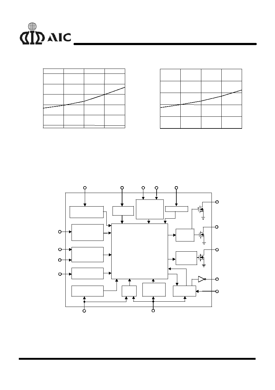
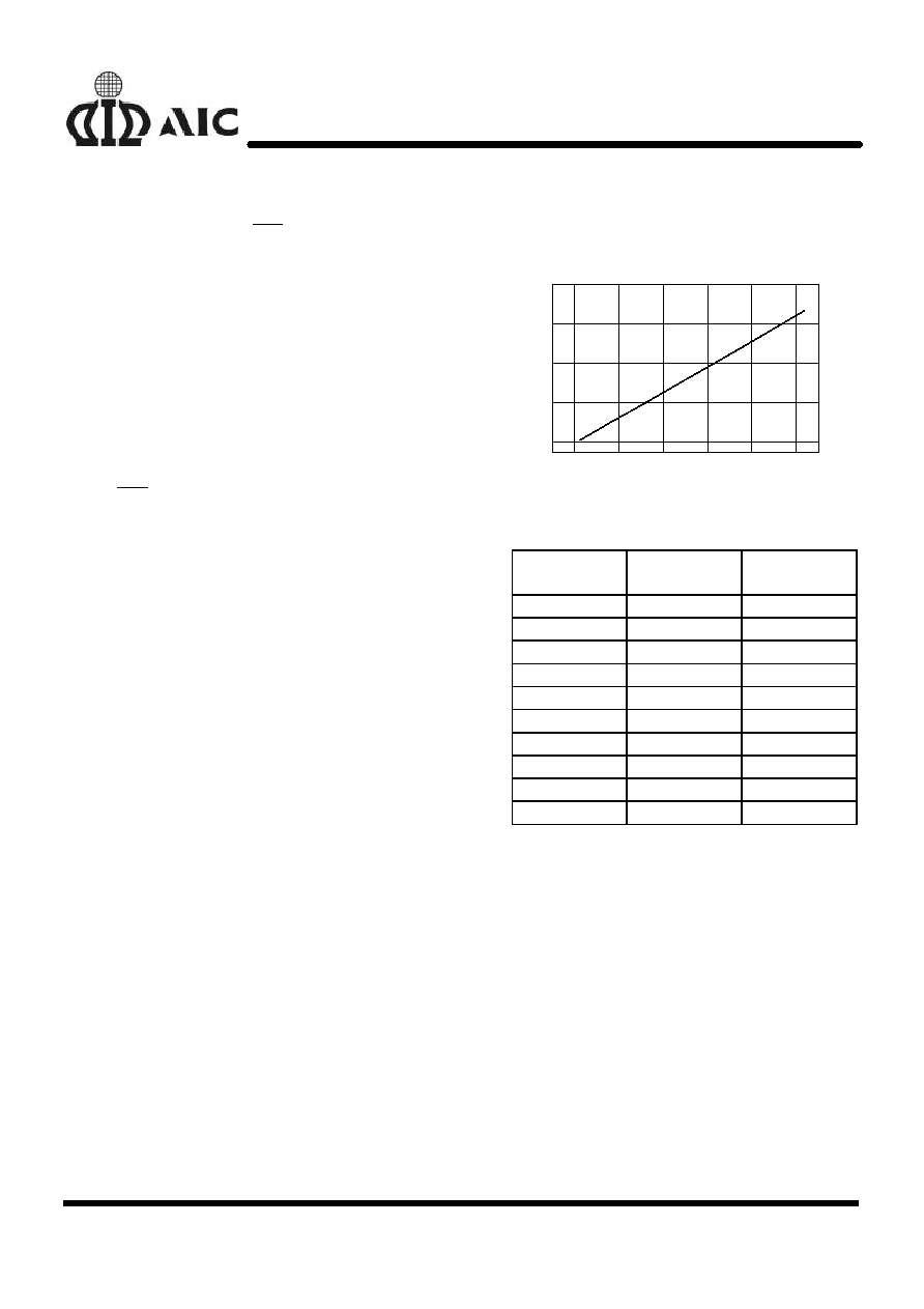
0
10
20
30
40
50
60
1.15
1.25
1.35
1.45
1.55
100
80
60
40
20
Temperature (
�
C
)
Temperature
Cell Voltage
Cell Voltage (V)
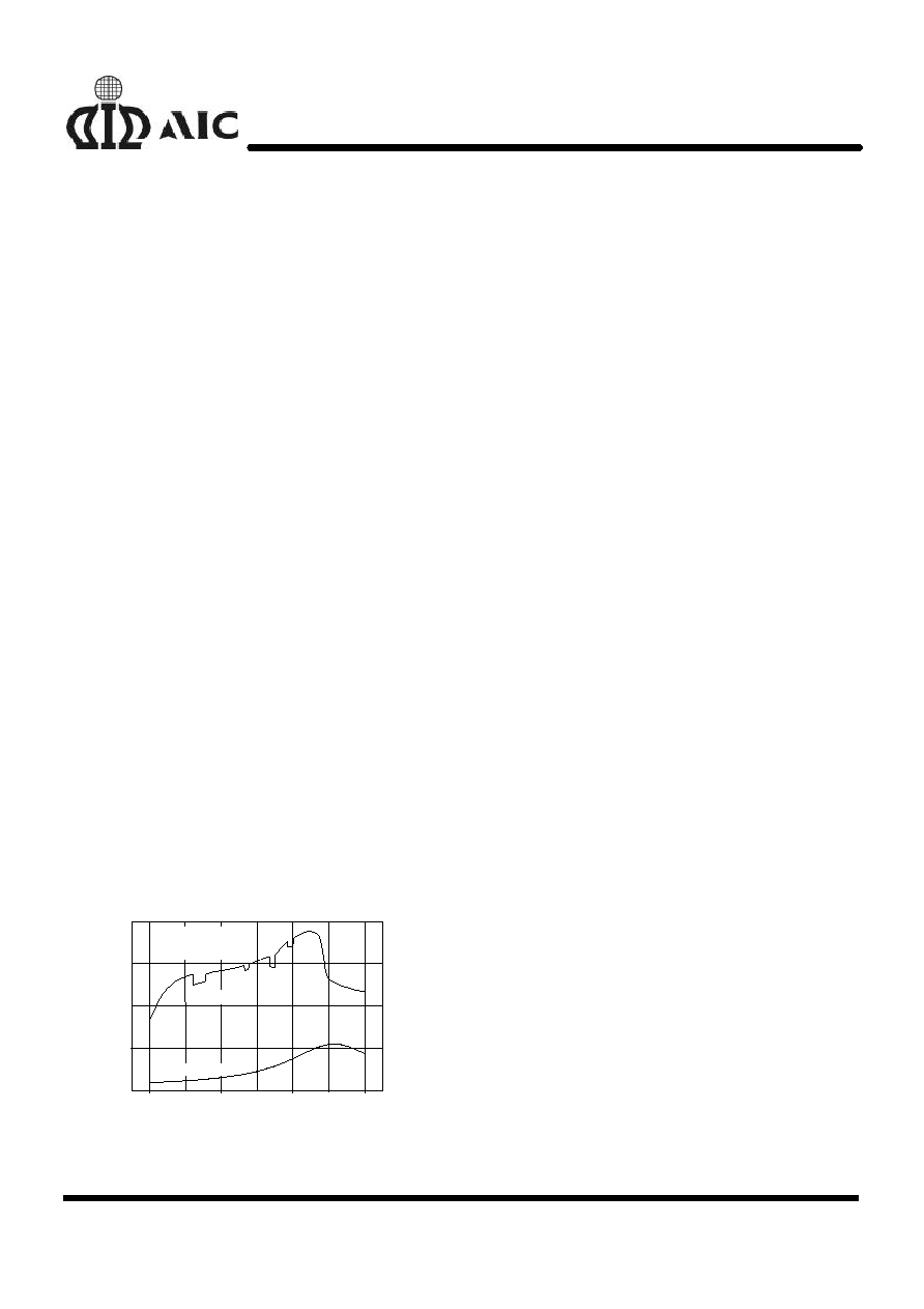
Charge Time (min.)
Charge Current = 600 mA
Cell Capacity = 550 mA
NiMH Battery
Fig. 1 Battery Charging Characteristics Resulting from
an AIC1781A-Controlled Charger with a
Fluctuating Charging Current
n
DESCRIPTION
The AIC1781A fast charge controller IC is
designed for intelligent charging of NiMH or NiCd
batteries without the risk of overcharge.
-
V
Detection (-0.25%), 0 V
detection (peak
voltage timer) and
T / t detection are the
primary methods employed by the AIC1781A to
terminate fast charge. The fast charge can also be
cut off by maximum battery voltage and maximum
battery temperature detection along with the
safety timer to prevent charging under fault
conditions of the charging system or the battery
itself.
Both
T / t and
-
V detection methods have
been proved powerful in terminating fast charging
for NiMH and NiCd batteries. The AIC1781A
utilizes the combination of these two methods to
achieve reliable decision of ending fast charge and
prevent misacting caused by using
-
V detection
alone under certain conditions. Fig. 1 shows an
example of charging curve of a battery charged by
a fluctuating current from a NiMH battery charger,
which uses the AIC1781A controller IC to achieve
optimal charging. This technique, in cooperating
with the 0 V
detection (peak voltage timer), is
particularly suitable for NiMH batteries, whose
voltage drop is hardly significant yet temperature
rises rapidly. The
T / t or
-
V detection
circuitry may be disabled independently for
different applications, such as system-integrated
chargers, chargers with varying charge current, or
battery packs lack of temperature sensing
thermistor.
The safety timer period, mode of battery
temperature protection, battery voltage protection
range, pulsed trickle charge duty, and LED display
mode are all adjustable or selectable.
AIC1781A
2
Discharge-before-charge function is included to
get rid of memory effect of NiCd batteries without
the risk of overdischarging. Test mode is provided
for charger manufactures to dramatically reduce
production test time.
n
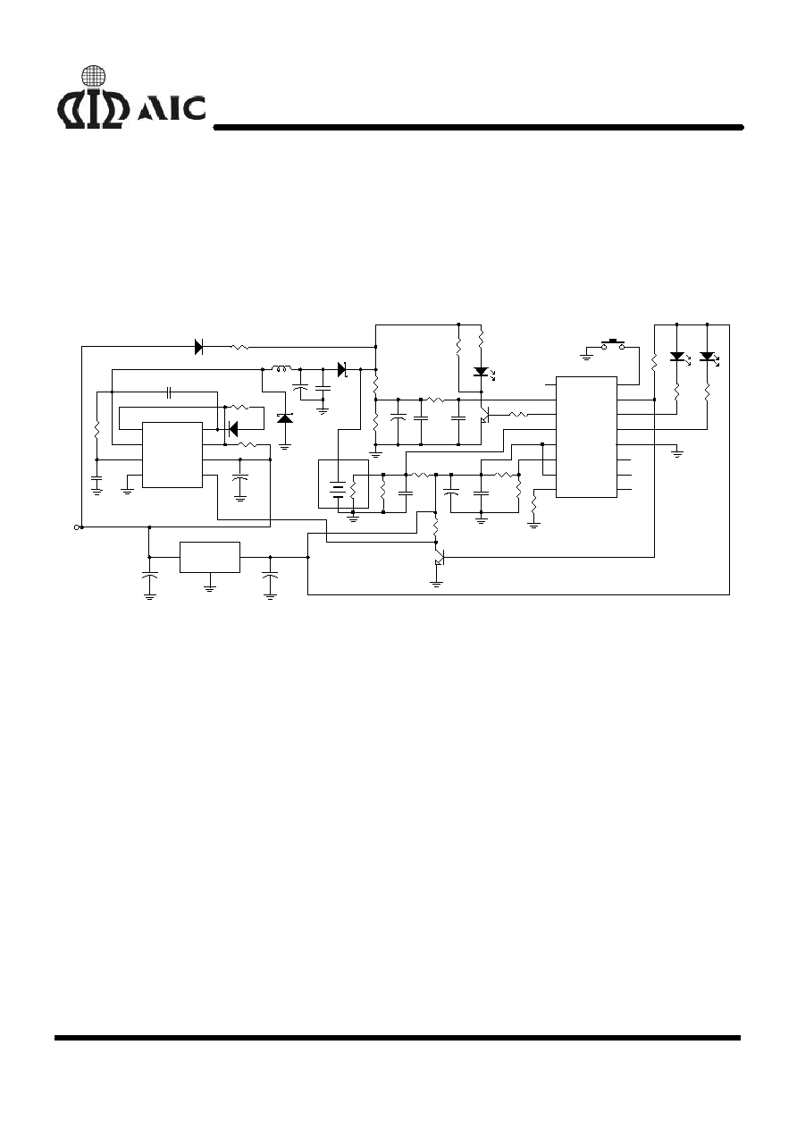
TYPICAL APPLICATION CIRCUIT
PEAK
1
VBT
2
DIS
3
VTS
4
VCC
5
ADJ
6
SEL3
7
TMR
8
MODE
9
SEL2
10
SEL1
11
GND
12
LED1
13
LED2
14
ICON
15
DSW
16
U2
AIC1781A
R8
300K
R9
91K
R10
100K
+
C9
4.7
�
F
C7
0.1
�
F
C10
47nF
R15
680
R3
270
R2
20/5W
SW1
PB SW
R12
100K
R16
680
R17
680
R14
200K
C8
0.
1
�
F
+
C11
100
�
F
RX
R11
100K
RY
C6
0.1
�
F
R13
470K
Q2
MMBT2222A
R6
50K
LED2
GREEN
LED3
RED
LED1
YELLOW
Q1
MPS2222A
+
C4
220
�
F
C5
0
.1
�
F
+
C12
1
�
F
+
C13
10
�
F
R5
120/0.5W
R1
1K
BAT1
**
B
ATTERY
R7
THERMISTOR
VIN
11~15V
L1
220
�
H
C2
1
�
F
C1
470P
RS
0.3/1W
1
2
3
GND
4
FB
5
VCC
DC
DE
CF
6
IS
7
BOOST
8
U1
AIC1563
+
C3
220
�
F
R4
390K
D3
IN4148
D1
IN4148
D2
IN5819
D4
1N5819
VIN
VOUT
GND
U3
78L05
**3~5 NiMH/NiCd cells.
Note: Charge Current=0.3/RS Ampere
Safety Timer: 80min
Battery Charge Circuit for Fluctuating Charging Current Application

AIC1781A
3
n
ORDERING INFORMATION
16
14
15
10
12
11
13
TOP VIEW
PIN CONFIGURATION
9
1
3
2
5
7
6
4
8
PEAK
VBT
DIS
VTS
VCC
ADJ
SEL3
SEL1
SEL2
MODE
LED1
GND
TMR
DSW
ICON
LED2
PACKING TYPE
TR: TAPE & REEL
TB: TUBE
PACKAGE TYPE
N: PLASTIC DIP
S: SMALL OUTLINE
C: COMMERCIAL
P: LEAD FREE COMMERCIAL
(Available for PS only)
Example: AIC1781CSTR
�
in SO-16 Package & Tape & Reel Packing Type
(CN is not available in TR packing type)
AIC1781PSTR
�
in SO-16 Lead Free Package & Tape & Reel
Packing Type
AIC1781AXXXX
n
ABSOLUTE MAXIMUM RATINGS
Supply Voltage
............................................... ... ... ... ........................................ 5.5V
DC Voltage Applied on any pin ......................... ... ... ... ... ...................................... 5.5V
Sink current of ICON pin, LED1 and LED2 pin .......................... ... ... .................. 20mA
Operating Temperature Range ........................................ ... ... ... ... .............. 0
�
C~ 70
�
C
Storage Temperature Range ................................................ ... ... ... ...... -65
�
C~ 150
�
C
n
TEST CIRCUIT
PEAK
DSW
VBT
ICON
DIS
LED2
VTS
LED1
VCC
GND
ADJ
SEL1
SEL3
SEL2
TMR
MODE
V2 (3V)
V1 (0.95V)
V
CC
V
CC
(5V)
V
CC
GREEN
ORANGE
RED
560
AIC1781A
R2
-
+
-
+
YELLOW
VOLTAGE
SOURCE
VOLTAGE SOURCE
V
CC
V
CC
V
CC
V
CC
100K
R1
560
560
R3
R4
560
R5
AIC1781A
4
n
ELECTRICAL CHARACTERISTICS
(T
A
=25
�
C, V
CC
=5V, unless otherwise specified.)
PARAMETER
TEST CONDITIONS
SYMBOL
MIN.
TYP.
MAX. UNIT
Supply Voltage
V
CC
4.5
5.0
5.5
V
Supply Current
I
CC
1.1
mA
Battery Low
During Initial Timer
0.11
0.16
0.21
After Initial Timer
(SEL3>3V)
0.63
0.69
0.75
(SEL3<2V)
1.1
1.2
1.30
Battery High
(SEL3>3V)
2.6
2.7
2.80
Voltage Protection Limit
(SEL3<2V)
V
BT
1.9
2.0
2.10
V
Temperature High
1.35
1.45
1.55
Temperature Sense Limit
Temperature Low
V
TS
3.5
3.6
3.70
V
Output impedance of DIS Pin
Z
DIS
50
100
LED1, LED2, ICON pins
Output Impedance
ON
OFF
1
25
50
M
Source Current Capability
SEL3 pin
DSW pin
I
SEL3
I
DSW
5.5
90
�
A
MODE, PEAK, SEL1,
SEL2 pins
300
K
Input Impedance
VBT, VTS, ADJ pins
1
M
Recommended External
Resistor of TMR pin
R
TMR
2
100
1000
K
-
V Detection Level w.r.t.*
Peak Value
-0.25
%
* w.r.t.: with respect to

AIC1781A
5
n
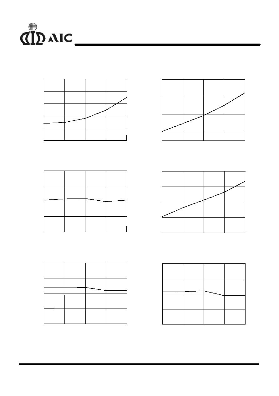
TYPICAL PERFORMANCE CHARACTERISTICS
(T
A
=25
�
C, R2=100K
, V
CC
=5V,
refer to Test Circuit)
4.4
4.6
4.8
5.0
5.2
5.4
0.84
0.90
0.96
1.02
1.08
Supply Current (mA)
V
CC
(V)
Fig. 2 Supply Current vs. Supply Voltage
Safety Timer (min)
V
CC
(V)
Fig. 3 Safety Timer vs. Supply Voltage
4.4
4.6
4.8
5.0
5.2
5.4
5.6
78.0
78.5
79.0
79.5
80.0
80.5
81.0
81.5
V
CC
(V)
Frequency (Hz)
Fig. 4 LED Flashing Frequency vs.
Supply Voltage
4.4
4.6
4.8
5.0
5.2
5.4
5.6
3.6
3.8
4.0
4.2
4.4
Supply Current (mA)
Temperature (
�
C)
Fig.5 Supply Current vs. Temperature
0
20
40
60
80
0.80
0.85
0.90
0.95
1.00
1.05
Temperature (
�
C)
Safety Timer (min)
Fig. 6 Safety Timer vs. Temperature
0
20
40
60
80
75
76
77
78
79
80
81
82
Frequency (Hz)
Temperature (
�
C)
Fig. 7 LED Flashing Frequency vs.
Temperature
-20
0
20
40
60
80
3.4
3.6
3.8
4.0
4.2
4.4
4.6
4.8
5.0
AIC1781A
6
n
TYPICAL PERFORMANCE CHARACTERISTICS
(Continued)
Temperature (
�
C)
V
BT
(V)
Fig. 8 VBT (High) Limit vs. Temperature
(SEL3>3V)
0
20
40
60
80
2.60
2.64
2.68
2.72
2.76
2.80
Temperature (
�
C)
V
BT
(V)
Fig. 9 VBT (High) Limit vs. Temperature
(SEL3<2V)
0
20
40
60
80
1.92
2.04
2.16
2.28
0
20
40
60
80
0.12
0.14
0.16
0.18
0.20
Temperature (
�
C)
V
BT
(V)
Fig.10 VBT (Low) Limit vs. Temperature
(During Initial Timer)
0
20
40
60
80
21
24
27
30
33
Temperature (
�
C)
Output Impedance (O)
Fig.11 Output Impedance vs. Temperature
(LED1, LED2, ICON Pins)
0
20
40
60
80
3.2
3.4
3.6
3.8
4.0
Temperature (
�
C)
V
BT
(V)
Fig.12 VTS (Low Temp) Limit vs.
Temperature
0
20
40
60
80
1.35
1.40
1.45
1.50
1.55
Temperature (
�
C)
V
TS
(
V
)
Fig.13 V
TS
(High Temp) Limit vs.
Temperature
AIC1781A
7
Temperature (
�
C)
V
BT
(V)
Fig. 14 V
BT
(Low) Limit vs. Temperature
(SEL3>3V, After Initial Timer)
0
20
40
60
80
0.
64
0.68
0.
72
0.
76
0.
80
0.8
4
Temperature (
�
C)
V
BT
(
V
)
Fig.15
VBT (Low) Limit vs. Temperature
(SEL3<2V, After Initial Timer)
0
20
40
60
80
1.0
1.1
1.2
1.3
1.4
1.5
n
BLOCK DIAGRAM
Charge Control
State Machine
SEL1
SEL2
ADJ
SEL3
ICON
LED1
LED2
VTS
VBT
DSW
DIS
Discharge
Control Unit
Battery
Voltage
Protection
13-bit
A/D
Battery Temp.
Protection
Display
Control
Unit
TMR
Oscillator
VCC
GND
Bandgap
Reference &
Voltage
Regulator
PEAK
MODE
MODE
Selection
Peak Voltage
Timer Control
Battery Voltage &
Temperature
Portection Setting
LED`s Display
& Trickle Pulse
Duty Setting
T/
t Detection
Setting
Charge
Control Unit

AIC1781A
8
n
PIN DESCRIPTIONS
PIN 1: PEAK- Tri-level input, determining the
period of peak voltage timer.
(See 0
V cut-off section in
application informations.)
PIN 2: VBT- Divided battery voltage input to
sense the battery voltage.
PIN 3: DIS-
Push-pull output, used to
control an external transistor to
discharge the battery. DIS is
active high when the
AIC1781A enters discharge
mode.
PIN 4: VTS- The battery cell temperature is
represented as a voltage input
to the AIC1781A at this pin.
The acceptable voltage range
of VTS pin is 0.29V
CC
to
0.72V
CC
. The battery
temperature is regarded as too
high if the voltage of VTS pin is
lower than 0.29V
CC
, and is
otherwise regarded as too low
if the voltage of VTS pin is
higher than 0.72V
CC
.
PIN 5: VCC- Power supply input at 5V
�
10%.
PIN 6: ADJ- For adjusting the slope of
T/
t.
Acceptable voltage range for
this pin is approximately 0.28V
to 3.8V. If voltage higher than
VCC-0.3V, the function of
T/
t detection is disabled.
PIN 7: SEL3-
Determine the acceptable
voltage range of VBT pin and
mode of temperature
protection function.
PIN 8: TMR- Determine the period of safety
timer with an external resistor
connected to GND.
PIN 9: MODE- Determine the mode of
operation for the AIC1781A.
PIN 10: SEL2 - Tri-level inputs, that jointly
control the LED display mode
and the duty of trickle charge
after the completion of fast
charge.
PIN 11: SEL1- The same as Pin 10.
PIN 12: GND- Power ground.
PIN 13: LED1 &
PIN 14: LED2- Open-drained outputs used to
indicate the battery charging
status. Two modes of display
are available, depending on
the setting of SEL1 and SEL2
pins.
PIN 15: ICON- Open-drained output, used to
control the charging current to
the battery.
PIN 16: DSW- Controlling the function of
discharge- before- charge.
(See discharge- before- charge
subsection in application
informations).

AIC1781A
9
n
APPLICATION INFORMATIONS
l
THE AIC1781A OPERATION
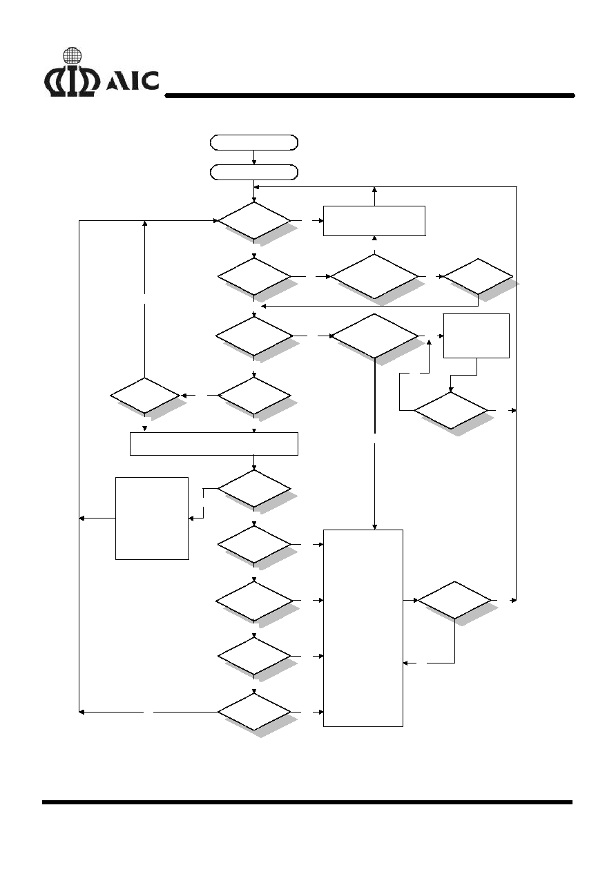
Power-on and Battery Pre-qualifying
When power is first applied to the AIC1781A, all
internal digital circuit blocks of the AIC1781A are
reset by the internal power-on-reset circuitry and
output LEDs (depending on the setting of SEL1 and
SEL2 pins) flash 3 times to indicate the initiation of
power-on. The internal control unit then examines
the battery condition through the VBT and VTS
pins.
The acceptable limits of VBT pin is determined by
the input voltage of SEL3 pin and the acceptable
temperature sense voltage window for VTS pin is
0.29 V
CC
to 0.72 V
CC
. If the voltage of VBT pin fails
to fall within the predetermined acceptable limits,
the AIC1781A enters a charge-suspending mode, in
which all the internal circuitry remains in reset state.
If the voltage of VTS pin is outside the 0.29 V
CC
to
0.72 V
CC
window, action of AIC1781A is determined
by the input voltage of SEL3 pin.
Discharge-Before-Charge
The AIC1781A provides the function of
discharge-before-charge to precondition NiCd
batteries which suffer from memory effect. This
function can only be activated after the
pre-qualification of battery voltage and temperature,
yet before the charge completion is registered for
the fast charge cycle.
To trigger this function, DSW pin has to be biased
to GND for over 0.18 second. After discharge
begins, LED1 and LED2 pins are both off, ICON
pin is on, and DIS pin goes high to activate an
external circuit to discharge the battery until the
voltage of VBT pin falls below 0.9V (or 0.69V,
depending on the input voltage of SEL3 pin) or
DSW pin is biased to GND for over 0.18 second
again. Fast charge will automatically start after
discharge is finished. The application circuit is
included in TYPICAL APPLICATION CIRCUIT.
Fast Charge
After the battery passes fault checks and required
discharging of the battery is completed, fast
charging begins while initial timer and safety timer
of the AIC1781A start counting. Functions of -
V
detection, peak voltage timer,
t
T/
detection,
and maximum battery voltage are, however,
disabled temporarily until the initial timer period in
the initial stage of a charge cycle elapses. The
initial timer period is equal to 1/80 of safety timer.
Since the low limit of acceptable VBT voltage is
only about 0.16V during the initial timer period,
even deeply discharged batteries can easily qualify
to be fast charged subsequently.
In the course of fast charge, the AIC1781A
constantly monitors the voltages at VBT and VTS
pins. The fast charge process is switched to trickle
charge when any one of the following situations is
encountered, which are explained below:
l
Negative delta voltage (-
V)
l
Peak voltage timer (0 V
)
l
Delta temperature/ delta time (
T/
t)
l
Maximum charge time
l
Maximum battery voltage
l
Maximum battery temperature
-
V Cutoff
The AIC1781A makes a voltage sampling at VBT
pin every 4 seconds when safety timer period is set
equal to 80 minutes. If a negative delta voltage of
0.25% compared to its peak value is detected at
VBT pin, the fast charge cycle is terminated.
0
V Cutoff
If the battery voltage stays at its peak value or
decreases very slowly for the duration determined
AIC1781A
10
by the peak voltage timer, which is in turn
determined by PEAK pin voltage, the fast charge
action is terminated.
T/
t Cutoff
The
t
T/
detection of the AIC1781A is performed
by sensing the decrease of VTS pin voltage in a
specific timer interval dictated by the safety timer.
The fast charging terminates when the decrease of
VTS pin voltage in 56 seconds exceeds the
predetermined value set by ADJ pin input. This time
interval of 56 seconds is based on the assumption
that voltage of VTS pin is sampled once for every 8
seconds, which is also determined by safety timer.
Functioning of -
V detection and peak voltage timer
(0 V
) can be disabled if the MODE pin is biased to
GND. Functioning of
t
T/
detection can be
disabled if the voltage of ADJ pin is higher than V
CC
- 0.3V.
Maximum Safety Timer Cutoff
The maximum fast charge period is determined by
the safety timer, which is set by a resistor
connected from TMR pin to GND. Safety timer, -
V
sampling rate, and
t
T/
sampling rate will be
longer if the resistor value is larger. When the value
of the resistor is 100K
, the safety timer period
equals 80 minutes. This can be verified by biasing
MODE pin to V
CC
and the measured frequency on
DSW pin should be around 32.8 KHz. After the
safety timer period is finished, the fast charge
action is terminated.
Maximum Voltage and Temperature Cutoff
The AIC1781A guards against the maximum limits
for battery voltage and temperature during fast
charging. If either of these limits is exceeded, fast
charge action is terminated.
Trickle Charge
There are five different selectable duty cycles for
trickle charge after the fast charge to prevent the
loss of charge due to battery self-discharging. The
duty cycle is controlled by the setting of SEL1 and
SEL2 pins.
The functions and charging states control
mentioned above are illustrated in the function flow
chart of AIC1781A (Fig. 16)
l
DESIGN GUIDE
Selecting Peak Voltage Timer (0
V)
The voltage of PEAK pin along with safety timer
determines the period of peak voltage timer. It can
be selected according to the following table:
TABLE 1
PEAK PIN
PEAK VOLTAGE TIMER
V
CC
1.5% of safety timer
Floating
3.7% of safety timer
GND
6% of safety timer
Battery Voltage Measurement
The AIC1781A measures the battery voltage
through VBT pin, which is connected to battery
positive terminal through a resistor-divider network,
as shown in Fig. 17. The input voltage of SEL3 pin
determines the acceptable limit of divided battery
voltage.
V
BAT
RA
RB
C5
4.7
�
F
2
R5
100K
C6
0.1
�
F
AIC1781A
VBT
+
Fig. 17 Battery Voltage Divider
For SEL3 > (V
CC
/2) + 0.4V, the suggested divider
resistance of RA and RB for the corresponding
number of battery cells are as below:

AIC1781A
11
TABLE 2
BATTERY
CELLS
RA/RB
RA (K
)
RB (K
)
2~4
2
240
120
3~6
3.3
300
91
4~8
4.9
300
62
5~10
6.4
300
47
6~12
7.8
310
39
8~16
10.8
390
36
For SEL3 < (V
CC
/2) -0.4V, the suggested divider
resistance of RA and RB for the corresponding
number of battery cells are as below:
TABLE 3
BATTERY
CELLS
RA/RB
RA(K
)
RB (K
)
2
1
240
240
3
2
240
120
4
3
240
80
5
4
300
75
6
5
300
60
8
7
360
51
10
9
360
40
12
11
390
36
16
15
410
27
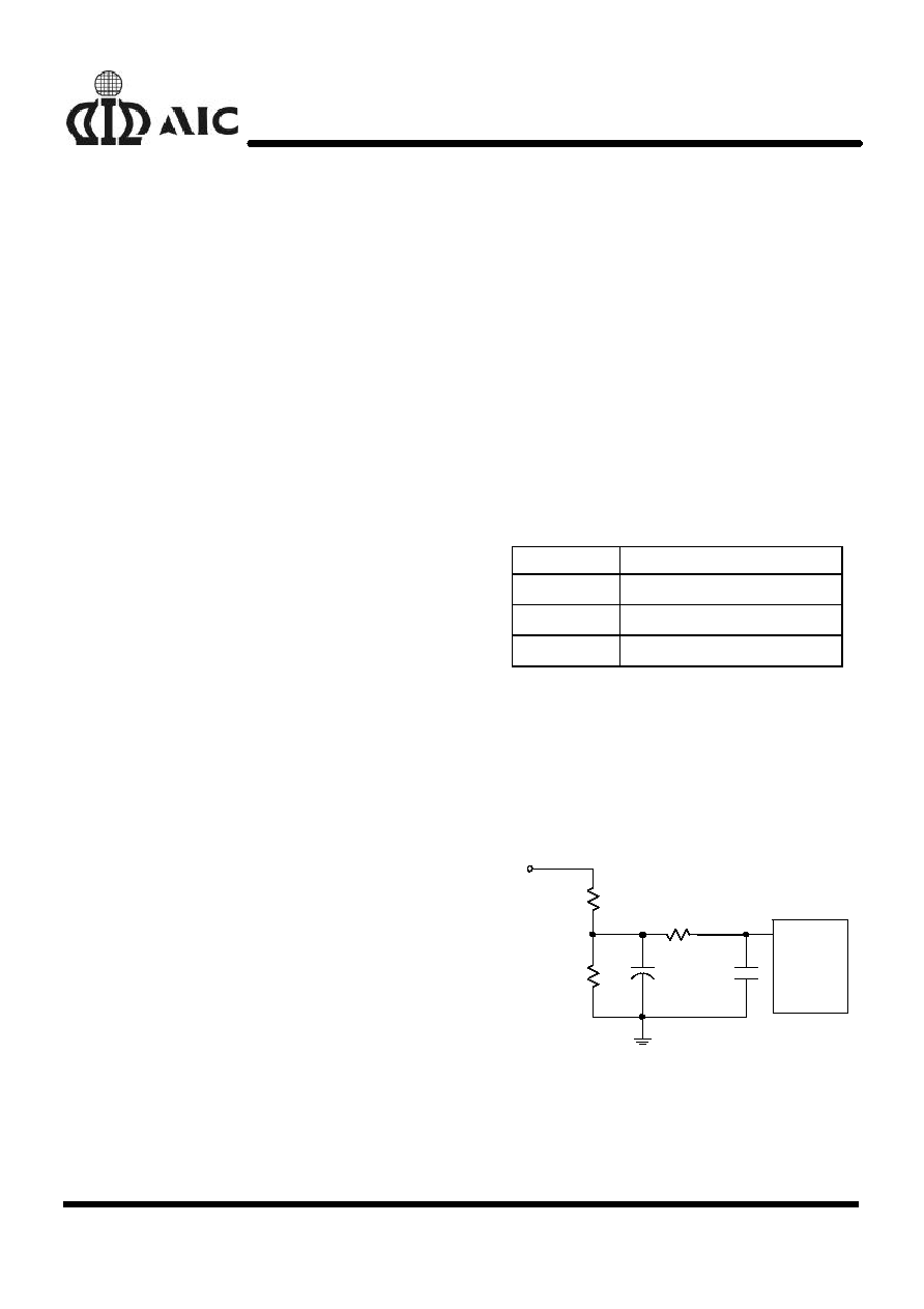
Battery Temperature Measurement
The AIC1781A employs a negative temperature
coefficient (NTC) thermistor to measure the
battery's temperature. The thermistor is inherently
nonlinear with respect to temperature. To reduce
the effect of nonlinearity, a resistor-divider network
in parallel with the thermistor is recommended. A
typical application circuit is shown in Fig. 18.
V
BAT
4
Rx
C7
0.1
�
F
V
CC
Ry
5
VCC
GND
12
Thermistor
VTS
AIC1781A
Fig. 18 Battery Temperature Sense Circuit
with a Negative Temperature Coefficient
(NTC) Thermistor
AIC1781A
12
Power ON
LED Flash 3 Times
If
VBT in Normal
Range
If
VNTC<0.72 VCC
If VNTC>0.29VCC
If
Discharge
Enabled
LED's Display Abnormal,
ICON ON,
Safety Timer Reset
If
SEL3>VCC-0.3V
or VCC/2-0.4V>SEL3
>1.4V
If
Discharge
Finished
LED's Display Fast Charge, ICON OFF
Safety Timer Counts
If
Initial Timer
Finished
If
Peak Timer Period
has Finished
If
0.25% Decline of VBT
is Detected
If
T/
t
has Reached
If
Safety Timer Period
has Finished
LED's Display
Battery Fulll,
Fast Charge
Finished,
Trickle charge
Starts
T/
t Detector,
-
V Detector,
Peak timer are all
Disabled
LED's Display,
Abnormal,
ICON ON,
Safety Timer Reset
If
SEL3>VCC-0.3V
or VCC/2-0.4V>SEL3
>1.4V
Battery Replacement
Battery Replacement
No
No
Yes
Yes
No
Yes
Yes
Yes
No
No
Yes
No
Yes
No
No
Yes
Yes
Yes
Yes
Yes
No
No
No
Yes
Yes
No
No
No
T/
t Disabled
Fig. 16 Function Flow Chart of AIC1781A
AIC1781A
13
The calculation for Rx and Ry in the circuit is as
following.
0.29 V
CC
=
)
R
(Ry//
Rx
Ry//R
TH
TH
+
x V
CC
R
TH
= The resistance of thermistor at upper limit of
temperature protection.
0.72 V
CC
=
)
R
(Ry//
Rx
Ry//R
TL
TL
+
x V
CC
R
TL
= The resistance of thermistor at lower limit of
temperature protection.
Substitution and rearranging the equations yield
Rx= 2.061
�
�
-
R
R
R
R
TL
TH
TL
TH
Ry =
5. 3
R
R
R
6. 3R
TL
TH
TL
TH
�
�
-
If temperature characteristic of the thermistor is like
that of SEMITEC 103AT-2, the resistance of Rx and
Ry is tabulated for different TL and TH as below.
(Note: TL is lower temperature limit and TH is upper
temperature limit.)
TABLE 4 Values of Rx and Ry at TL = 0
�
C
TH (
�
C)
Rx(K
)
Ry (K
)
50
10.1
551.1
51
9.7
300.7
52
9.4
204.8
53
9.0
153.9
54
8.7
122.8
55
8.4
101.8
56
8.1
86.5
57
7.8
75.0
58
7.5
66.0
59
7.2
58.7
60
7.0
52.8
61
6.8
47.8
62
6.5
43.6
63
6.3
39.9
64
6.1
36.8
65
5.9
34.0
66
5.7
31.6
67
5.5
29.5
68
5.3
27.5
69
5.2
25.8
70
5.0
24.3
TABLE 5 Values of Rx and Ry at TL = -10
�
C
TH (
�
C)
Rx (K
)
Ry (K
)
45
11.4
95.6
46
11.0
85.0
47
10.6
76.2
48
10.2
68.9
49
9.8
62.8
50
9.5
57.5
51
9.1
52.9
52
8.8
48.8
53
8.5
45.3
54
8.2
42.1
55
7.9
39.4
56
7.6
36.8
57
7.4
34.6
58
7.1
32.5
59
6.9
30.7
60
6.7
29.0
61
6.4
27.4
62
6.2
26.0
63
6.0
24.6
64
5.8
23.4
65
5.6
22.2
Setting the ADJ Pin Voltage
The slope of
T/
t detection is determined by ADJ
pin voltage of the AIC1781A.
The calculation of ADJ pin voltage is shown in the
following procedure followed by an example.
AIC1781A
14
Procedure
(a) First, determine the temperature protection
limits TH and TL. Then, substitute TH & TL into
the following equation:
TL
TH
0.43V
TL
TH
0.29V
0.72V
T
V
CC
CC
CC
BASE
TS
-
=
-
-
=
(b) Determine the safety timer to obtain the value of
t
BASE
.
.)
(min
Timer
Safety
.)
(min
80
56(sec.)
=
(sec.)
t
BASE
�
(c) Determine the expected slope of
T / t at
which temperature rises y
�
C in x seconds and
fast charge is subsequently cut off.
T
t
y
x
=
(d) Calculate the value of V
ADJ
BASE
BASE
TS
ADJ
t
t
T
T
V
30
V
�
�
�
=
Example
(a) Let TH=50
�
C, TL=0
�
C, V
CC
=5V. We have
V
T
0.43 5
50 0
0.043V/ C
TS
BASE
=
�
-
=
�
which means that V
TS
decreases 43mV as
temperature rises 1
�
C.
(b) If safety timer is equal to 80 minutes,
t
BASE
is
then 56 seconds.
(c) If fast charge should be terminated when
temperature rises 1
�
C in 60 seconds, then
0.0166
60
1
=
t
T/
=
(d) V
ADJ
=30 x 0.043x 0.0166 x 56 = 1.2(V)
If the temperature range is from 0
�
C to 50
�
C,
the voltage of V
ADJ
under different setting
conditions should be set as tabulated below.
TABLE 6 ADJ pin Voltage (TL=0
�
C, TH=50
�
C)
T / t
S.T.
0.75
(
�
C/min.)
1.0
(
�
C/min.)
1.25
(
�
C/min.)
40 min. (2C)
0.45
0.60
0.75
80 min. (1C)
0.90
1.20
1.50
120 min. (0.67C)
1.35
1.80
2.25
160 min. (0.5C)
1.80
2.40
3.01
200 min. (0.4C)
2.25
3.01
3.76
240 min. (0.33C)
2.70
3.61
4.51
A similar table for temperature range from 0
�
C to
60
�
C is as below.
TABLE 7 ADJ Pin Voltage (TL=0
�
C, TH=60
�
C)
T / t
S.T.
0.75
(
�
C/min.)
1.0
(
�
C/min.)
1.25
(
�
C/min.)
40 min. (2C)
0.37
0.50
0.62
80 min. (1C)
0.75
1.00
1.25
120 min. (0.67C)
1.12
1.50
1.88
160 min. (0.5C)
1.50
2.00
2.50
200 min. (0.4C)
1.88
2.50
3.13
240 min. (0.33C)
2.25
3.01
3.76
VBT Range and Temperature Protection
The acceptable voltage range of VBT pin and
mode of temperature protection function is
determined by the voltage of SEL3 pin, shown as
the following:
(a) SEL3 > V
CC
- 0.3V
Acceptable VBT Range:
Before initial timer: 0.16V~2.7V
After initial timer: 0.69V~2.7V
Temperature Protection Mode:
Entering charge-suspending mode when
temperature is either too low or too high,
same as abnormal battery voltage. Latch for
charge-suspending function is provided for
high temperature protection, but not for low
temperature protection.
AIC1781A
15
(b) V
CC
- 1.4V> SEL3 >
V
2
cc
+ 0.4V
Acceptable VBT Range:
Before initial timer: 0.16V~2.7V
After initial timer: 0.69V~2.7V
Temperature Protection Mode:
If temperature is too high, battery charging is
regarded as completed. If temperature is too
low, function of
T/
t detection is disabled, just
as thermistor is not existing.
(c)
V
2
cc
- 0.4V>SEL3 >1.4V
Acceptable VBT Range:
Before initial timer: 0.16V~2V
After initial timer: 1.2V~2V
Temperature Protection Mode:
Entering charge-suspending mode when
temperature is either too low or too high, same
as abnormal battery voltage. Latch for
charge-suspending function is provided for high
temperature protection, but not for low
temperature protection.
(d) 0.3V> SEL3
Acceptable VBT Range:
Before initial timer: 0.16V~2V
After initial timer: 1.2V~2V
Temperature Protection Mode:
If temperature is too high, battery charging is
regarded as completed. If temperature is too
low, function of
T/
t detection is disabled, just
as thermistor is not existing.
Setting the Period of Safety Timer
The AIC1781A provides a method for linearly
adjusting the period of safety timer with an external
resistor connected from TMR pin to GND. The
relation between safety timer length and the
external resistor (R
TMR
)
is shown in Fig. 19. The
table following shows the resistor values for some
of the commonly chosen safety timer periods. Also
shown in the table are their corresponding
oscillator frequencies.
0
100
200
300
400
500
0
200
400
600
800
R
TMR
(K
)
Safety Timer (min.)
Fig. 19 Safety Timer vs. R
TMR
TABLE 8
R
TMR
(K
)
OSC.
Freq.(KHz)
Safety timer
(min.)
11
256
10
23
131
20
48
65.8
40
74
43.1
60
100
32.8
80
152
21.6
120
206
16.0
160
314
10.6
250
491
6.89
380
667
5.04
520
Selecting Mode of Operation
The AIC1781A provides three modes of operation:
normal, test, and AC mode determined by the
setting of MODE pin according to TABLE 9. The
AIC1781A will operate normally when the MODE
pin is left floating (a 0.1
�
F capacitor is
recommended to be tied to MODE pin if the charge
circuit works in a noisy environment). When the
MODE pin is biased to GND, the function of -
V
detection is disabled. When the MODE pin is
biased to VCC, the AIC1781A enters the test mode.
The test mode can be used to significantly reduce
production test time. For relevant informations
please contact AIC directly.
AIC1781A
16
TABLE 9 The Operating Mode of AIC1781A
MODE pin
Mode Function
VCC
Test Safety timer period scaled
down to 1/32....etc.
Floating
Normal Normal operation
GND
AC
�
V detection disabled
The Mode of LED Display and Trickle Charge
The AIC1781A provides two LED display modes
and five-pulsed trickle charge modes. The
tri-level inputs, SEL1 and SEL2 pins, as in the
TABLE 6 determine the modes of LED display
and trickle charge.
TABLE 10 Mode of LED Display and Trickle
Charge
SEL1
SEL2
Trickle Charge
Duty
LED Display
Mode
V
CC
V
CC
Floating
GND
N/A
1/32
1/64
Type 1
Type 1
Type 1
Floating
V
CC
Floating
GND
1/128
1/256
N/A
Type 1
Type 1
Type 2
GND
V
CC
Floating
GND
1/32
1/64
1/128
Type 2
Type 2
Type 2
Display the Battery Charging Status
The AIC1781A provides two open-drained
outputs, LED1 and LED2, to indicate the battery
charging status. Refer to the table of LED display
mode (TABLE 10), depending on the setting of
SEL1 and SEL2 pins, the outputs of LED1 and
LED2 pins are shown in the following table:
TYPE 1
Power
ON
Fast
Charging
Charge
Completed
Fault
Conditions
LED1
1Hz
ON
OFF
OFF
LED2
OFF
OFF
ON
OFF
TYPE 2
Power
ON
Fast
Charging
Charge
Completed
Fault
Conditions
LED1
1Hz
ON
OFF
4Hz
Flashing
LED2
1Hz
4Hz
Flashing
ON
OFF
Charging Current Control
As shown in the typical application circuit, the
AIC1781A offers an open-drained output pin, ICON
pin, to control the charging current flow in fast
charge state and switch on to inhibit the charging
current flow in fault conditions. When fast charge is
completed, the AIC1781A enters the trickle charge
mode. In trickle charge mode, the ICON pin output
switches with predetermined duty cycle. Refer to
the table of trickle charge mode (TABLE 6), the
duty cycle is determined by the setting of SEL1
and SEL2 pins. The following table summarizes
how ICON pin corresponds to various charging
states.
Power
ON
Fast
Charging
Charge
Completed
Fault
Conditions
ICON
ON
OFF
See pin 10
& 11
ON
Test Mode
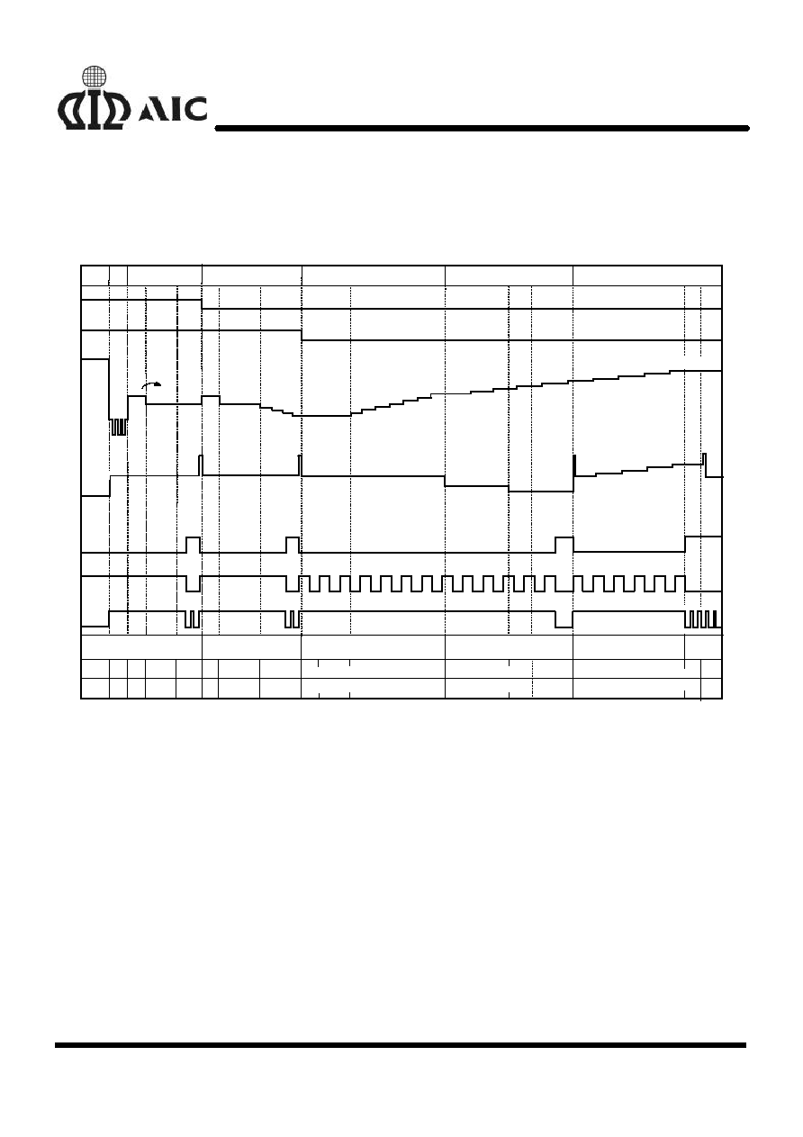
Fig. 20 shows the timing diagram for externally
controlled PEAK, ADJ, VBT, VTS, SEL1 and
SEL2 pin voltages of a recommended AIC1781A
test scheme, utilizing TEST mode function.
Output waveforms of LED1, LED2 and ICON of a
properly functioning AIC1781A are also shown in
the figure.
AIC1781A
17
n
TIMING DIAGRAM
Floating
Floating
SAFETY TIMER TEST
T/
t TEST
Floating
GND
Init.
GND
GND
GND
Floating
VCC
Floating
Floating
Floating
4V
(-0.15%)
(-0.15%)
(-2.5%)
4V
ON
OFF
4V
2mV
Step/100mS
2mV
Step/100mS
1.993V
(-0.35%)
2V
2V
1.95V
ON
1.97V
2V
4V
2V
1.9V
1.997V
1.997V
1.5V
VCC, SEL3, MODE=5V, (DSW FREQ.=820KHz, 25 TIMES of 32.8K)
(-2.15%)
0V
1.85V
5V
5V
1.12V
ON
ON
OFF
3.2KHz
ON
OFF
ON
T/
t INITIAL TIMER
OFF
OFF
PEAK TIMER TEST
-
V TEST
OFF
OFF
ON
2.14
9
0.4
8
0.12
4
0.28
0.12
2
0.02
10
0.32
5
0.32
0.7
0.32
0.2
3
0.24
0.1
0.5
7
0.12
6
5.92 6.02 6.04
3.78
3.38
3.14
2.64
1.94
1.62
0.74
0.54
1.5
1.18
0.86
0.26
0.14
0.14
1
ICON
VBT
ADJ
PEAK
LED2
LED1
VTS
TIME
(SEC.)
STAGE
SEL1
SEL2
OFF
ON
<2.1V
2V
Power
ON
3V
0V
0.1
0
2V
2V
Fig. 20 Timing Diagram of AIC1781A in Test Mode
AIC1781A
18
n
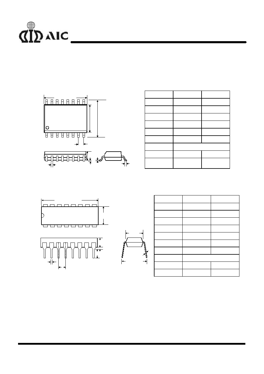
PHYSICAL DIMENSIONS
(unit: mm)
l
16 LEAD PLASTIC SO (300 mil) (CS) (PS)
SYMBOL
MIN
MAX
A
2.35
2.65
A1
0.10
0.30
B
0.33
0.51
C
0.23
0.32
D
10.10
10.50
E
7.40
7.60
e
1.27(TYP)
H
10.00
10.65
H
E
e
B
c
A
A1
D
L
L
0.40
1.27
l
16 LEAD PLASTIC DIP (CN)
SYMBOL
MIN
MAX
A1
0.381
--
A2
2.92
4.96
b
0.35
0.56
C
0.20
0.36
D
18.66
19.69
E
7.62
8.26
E1
6.09
7.12
e
2.54(TYP)
eB
--
10.92
b
e
L
A2
A1
eB
E
C
E1
D
L
2.92
3.81
Note:
Information provided by AIC is believed to be accurate and reliable. However, we cannot assume responsibility for use of any
circuitry other than circuitry entirely embodied in an AIC product; nor for any infringement of patents or other rights of third
parties that may result from its use. We reserve the right to change the circuitry and specifications without notice.
Life Support Policy: AIC does not authorize any AIC product for use in life support devices and/or systems. Life support devices
or systems are devices or systems which, (I) are intended for surgical implant into the body or (ii) support or sustain life, and
whose failure to perform, when properly used in accordance with instructions for use provided in the labeling, can be reasonably
expected to result in a significant injury to the user.