AIC1782
Dual-Battery Charge Controller
Analog Integrations Corporation 4F, 9, Industry E. 9th Rd, Science Based Industrial Park, Hsinchu Taiwan, ROC
www.analog.com.tw
DS-1782-00
TEL: 886-3-5772500 FAX: 886-3-5772510
1
FEATURES
Quick and Easy Testing for Production.
Sequential Charging Control of Two
NiMH/NiCd Battery Packs.
Reliable Sequential Fast Charge Control of
Dual NiMH and/or NiCd Battery Packs, even
with a Fluctuating Charging Current.
Fast Charge Termination by:
T / t ,
-V,
0 V
, Safety Timer, Maximum Temperature,
Maximum Voltage.
Safety Timer and
T / t Detection Slope
Linearly Adjustable.
Battery Voltage Protection Range Selectable.
Mode of Battery Temperature Protection Se-
lectable.
Protection against Battery Voltage and Battery
Temperature Faults.
Selectable LED Display Mode for Battery
Status.
Five Pulsed Trickle Charge Modes.
Discharge-before-Charge Function Available to
Eliminate Memory Effect.
20-pin DIP or SO Packages.
APPLICATIONS
Dual-Battery Fast Chargers for:
Mobile Phones.
Notebook and Laptop Personal Computers.
Portable Power Tools and Toys.
Portable Communication Equipments.
Portable Video & Stereo Equipments.
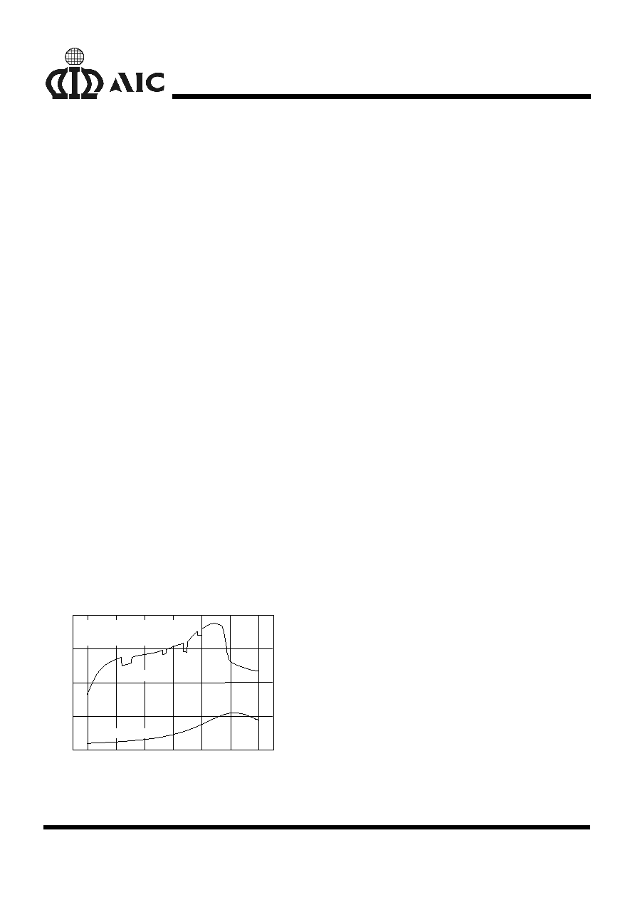
0
10
20
30
40
50
60
1.15
1.25
1.35
1.45
1.55
100
80
60
40
20
T
e
m
p
er
atur
e (
�
C)
C h a r g e C u r r e n t = 6 0 0 m A
C e l l C a p a c i t y = 5 5 0 m A
N i M H B a t t e r y
C e l l V o l t a g e
C
e
l
l
V
o
l
t
age (
V
)
C h a r g e T i m e ( mi n . )
T e m p e r a t u r e
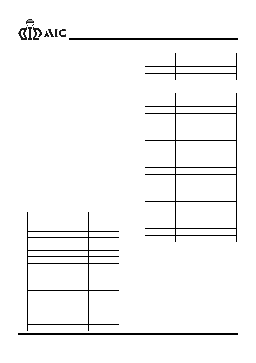
Fig. 1 Battery Charging Characteristics Resulted from
an AIC1782-Controlled Charger with a Fluc-
tuating Charging Current
DESCRIPTION
The AIC1782 fast charge controller is designed
for intelligent sequential charging of dual NiMH
and NiCd batteries without the risk of malfunction.
After powered on, the AIC1782 charging se-
quence gives priority to battery pack A, repre-
sented by input signals of ATS and ABV pins,
over battery pack B, represented by BTS and
BBV pin signals. The AIC1782 automatically
switches charging current to charge the standby
battery pack after the battery pack being charged
finishes its charging or encounters a fault condi-
tion.
-V (-0.25%) detection, 0 V
(peak voltage
timer) detection, and
T / t detection are the
primary methods employed by the AIC1782 to
terminate fast charge. The fast charge can also
be cut off by maximum battery voltage and
maximum battery temperature detection along
with the safety timer to prevent charging under
fault conditions of the charging system or the
battery itself
.
Both
T / t and
-V detection methods have
been proved powerful in terminating fast charging
for NiMH and NiCd batteries. The AIC1782 utilizes
the combination of these two methods to achieve
reliable decision of ending fast charge and prevent
misaction caused by using
-V detection alone
under certain conditions. Fig. 1 shows an example
of charging curve of a battery charged by a fluc-
tuating current from a NiMH battery charger which
uses the AIC1782 controller IC to achieve optimal
charging. The
T / t or
-V detection circuitry
may be disabled independently for different appli-
cations, such as system-integrated chargers,
chargers with varying charge current, or battery
packs lack of temperature sensing thermistor.
AIC1782
2
The safety timer period, mode of battery tem-
perature protection, battery voltage protection
range, pulsed trickle charge duty, and LED dis-
play mode are all adjustable or selectable. Dis-
charge-before-charge function is included to get
rid of memory effect of NiCd batteries without the
risk of overdischarging. Test mode is provided for
charger manufactures to dramatically reduce
production test time.
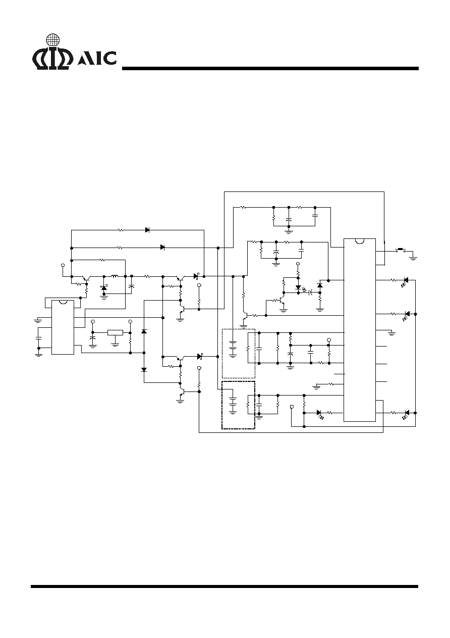
TYPICAL APPLICATION CIRCUIT
B2
R35
1
3
2
Q1
D468
R5
20/5W
R32
680
LED5
1M
R36
+
C1
4.7
�F
R1
R3
100K
R2
C2
0.1
�F
+
C3
4.7
�F
R6
R8 100K
R7
C4
0.1
�F
1.5K
R37
3.9K
R4
390
D8
1N4148
2.2
�F
C12
Q7
D468
VCC 5V
LED2
LED3
LED4
LED1
B1
D5
1N5820
D4
1N5820
D3
1N4148
D2
1N4148
Q3
3904
Q5
3904
D7
1N4148
D6
1N4148
D1
1N5821
L1
200
�H
+
C9
100
�F
+
C6
100
�F
+
C11
220
�F
Q4
A1012
Q2
A1012
Q6
A1012
R28
4.7K
R27
4.7K
R20
680
R19
680
R18
680
R17
680
R14
100K
R13
R34
1K
R25
470
R22
470
RS
0.1/2W
R29
150
R16
A
R15
R11
B
R12
R10
R24
2.7K
R21
2.7K
R33
47K
R26
330
R23
330
R30
220
C8
0.1
�F
C5
0.1
�F
C7
0.1
�F
C10
1nF
B
A
TTE
R
Y
B
AIC1782
SEL1
MODE
ICOA
LEA2
LEA1
ATS
TMR
SEL3
ADJ
VCC
SEL2
GND
BTS
DIS
LEB1
LEB2
ICOB
BBV
DSW
ABV
20
19
18
17
16
15
14
13
12
11
10
9
8
7
6
5
4
V
CC
(5V)
V
CC
(5V)
T
H
ER
M
I
ST
O
R
V
CC
(5V)
V
CC
(5V)
V
CC
(5V)
78L05
V
IN
V
IN
AIC1563
FB
VCC
IS
BST
GND
TC
SE
SC
B
A
TTE
R
Y
A
T
H
ER
MI
ST
O
R
SW1
+
Battery Charger for Dual NiMH and NiCd Battery
AIC1782
3
ORDERING INFORMATION
PACKAGE TYPE
N: PLASTIC DIP
S: SMALL OUTLINE
TEMPERATURE RANGE
C= 0
�C~70�C
ORDER NUMBER
AIC1782 CN
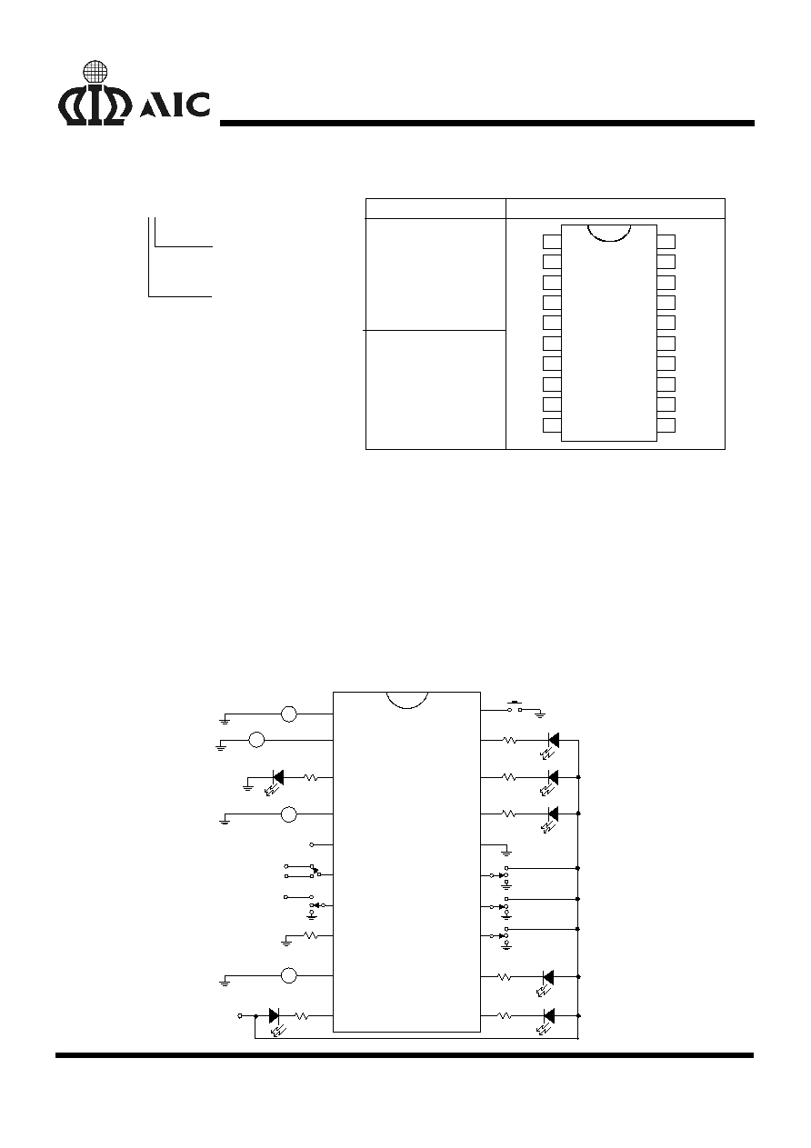
PIN CONFIGURATION
AIC1782 XX
(PLASTIC DIP)
AIC1782 CS
(PLASTIC SO)
1
3
2
16
14
15
5
7
6
10
12
11
4
8
13
9
ABV
BBV
DIS
BTS
VCC
ADJ
SEL3
SEL1
SEL2
LEB1
GND
TMR
DSW
ICOB
LEB2
17
20
19
18
MODE
ICOA
LEA2
ATS
LEA1
ABSOLUTE MAXIMUM RATINGS
Supply Voltage
................................................................................................... 5.5V
DC Voltage Applied on any Pin
........................................................................... 5.5V
Sink Current of ICOA Pin, LEA1 and LEA2 Pins ............................................... 20mA
Sink Current of ICOB Pin, LEB1 and LEB2 Pins ............................................... 20mA
Operating Temperature Range
................................................................... 0
�C~ 70�C
Storage Temperature Range ................................................................
-65
�C~ 150�C
TEST CIRCUIT
ABV
DSW
BBV
ICOB
DIS
LEB2
BTS
LEB1
VCC
GND
ADJ
SEL1
SEL3
SEL2
TMR
MODE
ATS
ICOA
LEA1
LEA2
V2 (3V)
V1 (0.95V)
V
CC
(5V)
GREEN
ORANGE
AIC1782
R2
-
+
YELLOW
Voltage Source
-
+
Voltage Source
V
CC
V
CC
100K
R1
560
560
R3
R4
560
-
+
Voltage Source
-
+
Voltage
Source
560
560
GREEN
ORANGE
R5
R8
R7
560
R6
V
CC
RED
560
RED
V
CC
V
CC
AIC1782
4
ELECTRICAL CHARACTERISTICS
(Ta=25
�
�
�
�C, V
CC
=5V, unless otherwise speci-
fied.)
PARAMETER
TEST CONDITIONS
SYMBOL
MIN.
TYP.
MAX.
UNIT
Supply Voltage
V
CC
4.5
5
5.5
V
Supply Current
I
CC
1.1
mA
Battery Low
V
ABV
Before Initial Timer
V
BBV
0.11
0.16
0.21
After Initial Timer
(SEL3>3V)
0.63
0.69
0.75
(SEL3<2V)
1.1
1.2
1.3
Battery High
(SEL3>3V)
2.6
2.7
2.8
Voltage Protection Limit
(SEL3<2V)
1.9
2.0
2.1
V
Temperature High
V
ATS
1.35
1.45
1.55
Temperature Sense
Limit
Temperature Low
V
BTS
3.5
3.6
3.7
V
Output impedance of DIS
Pin
Z
DIS
140
250
LEA1, LEA2, LEB1,
LEB2, ICOA, ICOB pins
Output Impedance
ON
OFF
1
25
50
M
Source Current
Capability
SEL3 pin
DSW pin
I
SEL3
I
DSW
5.5
16
�A
�A
MODE, SEL1, SEL2
pins
300
K
Input Impedance
ABV, BBV, ATS, BTS,
ADJ pins
1
M
Recommended External
Resistor of TMR pin
R
TM
R
2
100
1000
K
-V detection level w.r.t.*
Peak Value
-0.25
%
*: with respected to
AIC1782
5
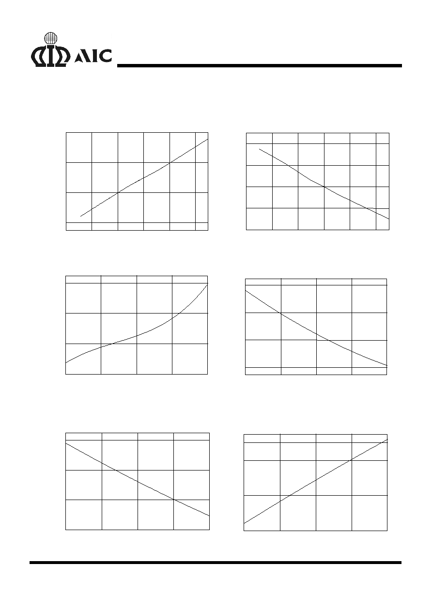
TYPICAL PERFORMANCE CHARACTERISTICS
(Ta=25
�
�
�
�C, R2=100K
,
V
CC
=5V, refer to Test Circuit)
4.4
4.6
4.8
5.0
5.2
5.4
1.00
1.06
1.12
1.18
Supply Current vs Supply Voltage
Su
p
p
l
y
C
u
rr
e
n
t
(mA
)
V
CC
(V)
79.0
79.5
80.0
80.5
81.0
4.4
4.6
4.8
5.0
5.2
5.4
Safety Timer vs Supply Volatge
S
a
fe
ty
Ti
m
e
r
(
m
i
n
.
)
V
CC
(V)
0
20
40
60
80
79.0
80.0
81.0
82.0
Safety Timer vs Temperature
S
a
fe
ty
T
i
m
e
r
(
m
i
n
.
)
Temperature(
�C)
1.02
0
20
40
60
80
0.90
1.14
1.26
Supply Current vs Temperature
S
u
p
p
l
y
Cur
r
en
t (
m
A
)
Temperature (
�C)
0
20
40
60
80
2.74
2.62
2.66
2.70
ABV and BBV (High) Limit vs Temperature
(SEL3>3V)
AB
V,
B
B
V
(
V
)
Temperature (
�C)
0
20
40
60
80
2.02
2.03
1.98
2.00
ABV and BBV (High) Limit vs Temperature
(SEL3<2V)
ABV,
BBV
(
V
)
Temperature (
�C)
AIC1782
6
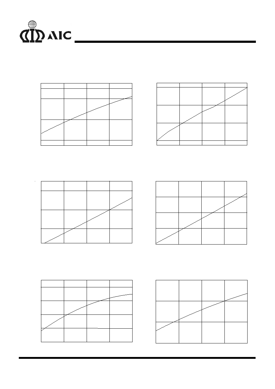
TYPICAL PERFORMANCE CHARACTERISTICS
(Continued)
ABV and BBV (Low) Limit vs Temperature
(Before Initial Timer)
ABV,
BBV (
V
)
0
20
40
60
80
0.158
0.160
0.162
0.163
Temperature (
�C)
23
25
27
29
0
20
40
60
80
Output Impedance vs Temperature
(LEA's, LEB's, ICO's pins)
O
u
t
put
I
m
pedanc
e(
)
Temperature(
�C)
ABV and BBV (Low ) limits vs Temperature
(SEL3<2V, After Initial Timer)
ABV
,
BBV
(
V
)
Temperature (
�C)
1.20
1.21
1.22
1.19
0
80
20
40
60
ABV and BBV (Low) limits vs Temperature
(SEL3>3V, After Initial Timer)
AB
V,
BB
V (
V
)
Temperature (
�C)
0
20
40
60
80
0.690
0.695
0.700
0.705
0.710
0
20
40
60
80
3.58
3.59
3.60
3.61
3.62
ATS and BTS (High) Limit vs Temperature
ATS,
B
T
S
(
V
)
Temperature (
�C)
0
20
40
60
80
1.42
1.44
1.46
1.48
ATS and BTS (Low) Limit vs Temperature
AT
S,
BT
S
(
V
)
Temperature (
�C)
AIC1782
7
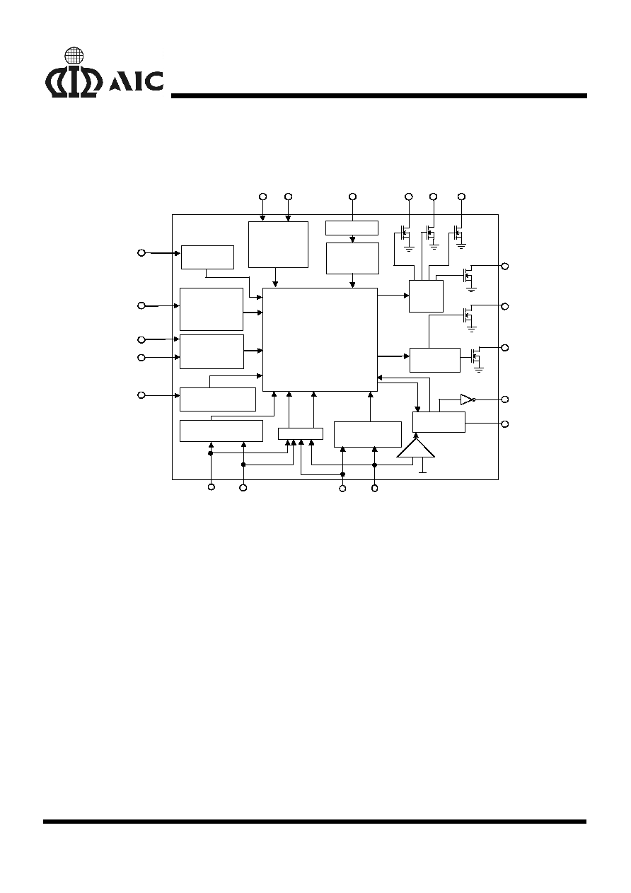
BLOCK DIAGRAM
LEB2 LEB1
LEA2
LEA1
ICOB
ICOA
Display
Control
Unit
TMR
Timing
Control Unit
GND VCC
Bandgap
Reference
& Voltage
Regulator
MODE
MODE
Selection
SEL3
Battery Voltage
& Temperature
Protection
Setting
SEL2
SEL1
LED Display&
Trickle Charge
Duty Setting
Charge Control
State Machine
CHARGE END
DSW
DIS
BBV
ATS
ADJ
Charge
Control Unit
T/t Detection
Setting
Battery Temperature
Protection
Battery Voltage
Protection
Discharge
Control Unit
13-bit A/D
Oscillator
+
-
BTS
ABV
PIN DESCRIPTIONS
PIN 1: ABV - Divided battery voltage input to
sense the battery voltage of
pack A.
PIN 2: BBV - Divided battery voltage input to
sense the battery voltage of
pack B.
PIN 3: DIS
- Push-pull output, used to con-
trol an external transistor to dis-
charge the battery of pack B.
DIS is active high when function
of discharge is enabled.
PIN 4: BTS - The battery cell temperature of
pack B is represented as a volt-
age input to the AIC1782 at this
pin. The acceptable voltage
range of BTS pin is 0.29 V
CC
to
0.72 V
CC
.
PIN 5: VCC
- Power supply input at 5V �
10%.
PIN
6: ADJ
- For adjusting the slope of
T / t . Acceptable voltage
range for this pin is approxi-
mately 0.28V to 3.8V. If volt-
age higher than VCC - 0.3V,
function of
T / t detection is
disabled.
PIN
7: SEL3
- Determining the acceptable
voltage range of ABV and
BBV pins and mode of tem-
perature protection function.

AIC1782
8
PIN
8: TMR
- Determining the period of
safety timer with an external
resistor connected to GND.
PIN 9: ATS
- The battery cell temperature
of pack A is represented as a
voltage input to the AIC1782
at this pin. the acceptable
voltage range of ATS is 0.29
V
CC
to 0.72 V
CC
.
PIN 10: LEA1 &
PIN 11: LEA2
- Open-drained outputs used to
indicate the charging status of
the battery pack A.
PIN 12: ICOA - Open-drained output, used to
control the charging current of
the battery pack A.
PIN 13: MODE - Determining the mode of op-
eration for the AIC1782.
PIN 14: SEL2 &
PIN
15: SEL1
- Tri-level inputs, that jointly
control the LED display mode
and the duty of trickle charge
after the completion of fast
charge.
PIN 16: GND
- Power ground.
PIN 17: LEB1 &
PIN 18: LEB2
- Open-drained outputs used to
indicate the charging status of
battery pack B
PIN 19: ICOB
- Open-drained output, used to
control the charging current of
the battery pack B.
PIN 20: DSW
- Controlling the function of dis-
charge-before-charge of the
battery pack B. (See dis-
charge-before-charge sub-
section in application informa-
tions).
APPLICATION INFORMATIONS
THE AIC1782 OPERATION
Power-on and Battery Prequalifying
The AIC1782 is a sequential charger, initiating a
charge action on either battery pack A or B.
When power is first applied to the AIC1782, all
internal digital circuit of the AIC1782 are reset
by the internal power-on-reset circuitry, the out-
put of LED`s (depending on the setting of SEL1
and SEL2 pins) flash 3 times to indicate the ini-
tiation of power-on. If both battery pack A and B
are present when V
CC
is applied to the AIC1782,
the charge action begins with battery pack A if
conditions are acceptable.
Condition of battery pack A is examined through
the ATS and ABV pins, while battery pack B is
examined through the BTS and BBV pins. The
acceptable limits of ABV and BBV are deter-
mined by the input voltage of SEL3 pin and the
acceptable temperature sense voltage window
for ATS and BTS are 0.29 V
CC
to 0.72 V
CC.
The AIC1782 controls the initiation of a charge
action and checks for acceptable battery volt-
age and temperature prior to fast charging. If
the voltage of ABV or BBV fail to fall within the
predetermined acceptable limits, the corre-
sponding battery pack enters a charging-
suspending mode. If the voltage of ATS or BTS
is outside the 0.29 V
CC
to 0.72 V
CC
window, ac-
tion to AIC1782 is determined by the input volt-
age of SEL3 pin.
Discharge-Before-Charge

AIC1782
14
The AIC1782 provides the function of dis-
charge-before-charge to precondition NiCd
batteries which suffer from memory effect. This
function can only be activated for pack B after
the prequalification of battery voltage and tem-
perature, yet before the charge completion is
registered for fast charge cycle of pack B.
To trigger this function, DSW pin has to be bi-
ased to GND over 0.18 second. After discharge
begins, LEB1 and LEB2 pins are both OFF,
ICOB pin is ON, and DIS pin goes high to acti-
vate an external circuit to discharge the battery
pack B until the voltage of BBV pin fall below
0.9V (or 0.69V, depending on the input voltage
of SEL3 pin) or DSW pin is biased to GND for
over 0.18 second again. The application circuit
is included in TYPICAL APPLICATION
CIRCUIT.
Fast Charge
After the battery passes fault checks, charge
begins on either of the batteries, the other bat-
tery remains in a waiting state until the first bat-
tery terminates fast charge. The AIC1782 will
automatically switch to fast charge the second
battery. The battery pack A has the priority over
battery pack B only when power is first applied
to the AIC1782. When fast charging begins, the
initial and safety timer of the AIC1782 start
counting. Functions of -
V detection, Peak volt-
age timer,
T / t detection, and maximum
battery voltage are, however, disabled tempo-
rarily until the initial timer period in the initial
stage of a charge cycle elapses. The initial timer
period is equal to 1/80 of safety timer.
Since the low limit of acceptable ABV or BBV
voltage are only about 0.16V during the initial
timer period, even deeply discharged batteries
can easily qualify to be fast charged subse-
quently.
In the course of fast charge, the AIC1782 con-
stantly monitors the battery voltage and tem-
perature through ABV (or BBV) and ATS (or
BTS) pins. The fast charge process is regis-
tered complete when any one of the following
situations is encountered, which are explained
below:
Negative delta voltage (-
V).
Peak voltage timer (0 V
).
Delta temperature/ delta time (
T / t ).
Maximum charge time.
Maximum battery voltage.
Maximum battery temperature.
-
V Cutoff
The AIC1782 makes a voltage sampling at ABV
(or BBV) pin every 4 seconds when safety timer
period is set equal to 80 minutes. If a negative
delta voltage of 0.25% compared to its peak
value is detected at ABV (or BBV) pin, the fast
charge cycle is terminated.
0
V Cutoff
If the battery voltage stays at its peak value or
decreases very slowly for the duration deter-
mined by the peak voltage timer, which is in turn
equal 3.7% of safety timer, the fast charge ac-
tion is terminated.
T/t Cutoff
The
T / t detection of the AIC1782 is per-
formed by sensing the decrease of ATS (or BTS)
pin voltage in a specific timer interval dictated
by the safety timer. The fast charging termi-
nates when the decrease of ATS (or BTS) pin
voltage in 56 seconds exceeds the predeter-
mined value set by ADJ pin input. This time in-
terval of 56 seconds is based on the assump-
tion that voltage of ATS (or BTS) pin is sampled
once for every 8 seconds, which is also deter-
mined by safety timer.

AIC1782
15
Functioning of -
V detection and peak voltage
timer (0 V
) can be disabled if the MODE pin is
biased to GND. Functioning of
T / t detection
can be disabled if the voltage of ADJ pin is
higher than V
CC
- 0.3V.
Maximum Safety Timer Cutoff
The maximum fast charge period is determined
by the safety timer, which is set by a resistor
connected from TMR pin to GND. Safety timer,
-
V sampling rate, and
T / t sampling rate
will be longer if the resistor value is larger.
When the value of the resistor is 100K
, the
safety timer period equals 80 minutes. This can
be verified by biasing MODE pin to V
CC
and the
measured frequency on DSW pin should be
around 32.8 KHz. After the safety timer period is
finished, the fast charge action is terminated.
Maximum Voltage and Temperature Cutoff
The AIC1782 guards against the maximum
limits for battery voltage and temperature during
fast charging. If either of these limits is ex-
ceeded, fast charge action is terminated.
Trickle Charge
There are five different selectable duty cycles
for trickle charge after the fast charge to prevent
the loss of charge due to battery self-
discharging. The setting of SEL1 and SEL2 pins
controls the duty cycle
.
This function can only
be activated on the following three situation:
Battery pack A is charge full and battery
pack B is abnormal.
Battery pack B is charge full and battery
pack A is abnormal.
Battery pack A and B are both charge full.
DESIGN GUIDE
ABV/BBV Range and Temperature Protec-
tion
The acceptable battery voltage range of ABV
and BBV pins and mode of temperature protec-
tion function is determined by the voltage of
SEL3 pin, shown as the following:
(a) SEL3 > V
CC
- 0.3V
Acceptable ABV/BBV Range:
Before initial timer: 0.16V~2.7V
After initial timer: 0.69V~2.7V
Temperature Protection Mode:
Entering charge-suspending mode when tem-
perature is either too low or too high, same as
abnormal battery voltage. Latch for charge-
suspending function is provided for high tem-
perature protection, but not for low temperature
protection.
(b) V
CC
- 1.4V> SEL3 >
V
2
cc
- 0.4V
Acceptable ABV/BBV Range:
Before initial timer: 0.16V~2.7V
After initial timer: 0.69V~2.7V
Temperature Protection Mode:
If temperature is too high, battery charging
is regarded as completed. If temperature is
too low, function of
T / t detection is
disabled, just as thermistor is not existing.
(c)
V
2
cc
- 0.4V>SEL3 >1.4V
Acceptable ABV/BBV Range:
Before initial timer: 0.16V~2 V
After initial timer:1.2V~2V
Temperature Protection Mode:
Entering charge-suspending mode when
temperature is either too low or too high,
same as abnormal battery voltage. Latch
for charge-suspending function is provided
for high temperature protection, but not for
low temperature protection.
AIC1782
16
(d) 0.3V> SEL3
Acceptable ABV/BBV Range:
Before initial timer: 0.16V~2 V
After initial timer:1.2V~2V
Temperature Protection Mode:
If temperature is too high, battery charging
is regarded as completed. If temperature is
too low, function of
T / t detection is
disabled, just as thermistor is not existing.
Battery Voltage Measurement
The AIC1782 measures the battery voltage
through ABV and BBV pins, which is connected
to battery positive terminal through a resistor-
divider network, as shown in Fig. 2. The ac-
ceptable limit of divided battery voltage is de-
termined by the input voltage of SEL3 pin.
V
BAT
RA
RB
C5
4.
7
�
F
R6
100K
C6
0.
1
�
F
AIC1782
ABV/BBV
+
Fig. 2 Battery Voltage Divider
For SEL3 > (VCC/2) + 0.4V, the suggested di-
vider resistances of RA and RB for the corre-
sponding number of battery cells are as below:
BATTERY
CELLS
RA/RB
RA (K
) RB (K)
2~4
2
240
120
3~6
3.3
300
91
4~8
4.9
300
62
5~10
6.4
300
47
6~12
7.8
310
39
8~16
10.8
390
36
For SEL3 < (V
CC
/2) -0.4V, the suggested divider
resistances of RA and RB for the corresponding
number of battery cells are as below:
BATTERY
CELLS
RA/RB
RA(K
)
RB (K
)
2
1
240
240
3
2
240
120
4
3
240
80
5
4
300
75
6
5
300
60
8
7
360
51
10
9
360
40
12
11
390
36
16
15
410
27
Battery Temperature Measurement
The AIC1782 employs a negative temperature
coefficient (NTC) thermistor to measure the
battery
'
s
temperature. The thermistor is inher-
ently nonlinear with respect to temperature. To
reduce the effect of nonlinearity, a resistor-
divider network in parallel with the thermistor is
recommended. A typical application circuit is
shown in Fig. 3.
V
BAT
Rx
C7
0.
1
�
F
V
CC
Ry
5
VCC
GND
16
T
h
er
m
i
s
t
or
ATS/BTS
AIC1782
Fig. 3 Battery Temperature Sense Circuit
with a Negative Temperature Coef-
ficient (NTC) Thermistor
AIC1782
17
The calculation for Rx and Ry in the circuit is as
following.
0.29 Vcc
Ry / /R
Rx (Ry / / R
)
Vcc
TH
TH
=
+
�
R
TH
= The resistance of thermistor at upper limit
of temperature protection.
0.72 Vcc
Ry / /R
Rx (Ry / / R )
Vcc
TH
TL
=
+
�
R
TL
= The resistance of thermistor at lower limit
of temperature protection.
Substitution and rearranging the equations yield
Rx= 2.061
�
�
-
R
R
R
R
TL
TH
TL
TH
Ry =
5. 3
R
R
R
6. 3R
TL
TH
TL
TH
�
�
-
If temperature characteristic of the thermistor
is like that of SEMITEC 103AT-2, the resis-
tance of Rx and Ry is tabulated for different
TL and TH as below.
(note: TL is lower temperature limit and TH is
upper temperature limit.)
TABLE. 1 Values of Rx and Ry at TL = 0
�
�
�
�C
TH (
�C)
Rx(K
)
Ry (K
)
50
10.1
551.1
51
9.7
300.7
52
9.4
204.8
53
9.0
153.9
54
8.7
122.8
55
8.4
101.8
56
8.1
86.5
57
7.8
75.0
58
7.5
66.0
59
7.2
58.7
60
7.0
52.8
61
6.8
47.8
62
6.5
43.6
63
6.3
39.9
64
6.1
36.8
65
5.9
34.0
66
5.7
31.6
67
5.5
29.5
68
5.3
27.5
69
5.2
25.8
70
5.0
24.3
TABLE. 2 Values of Rx and Ry at TL = -10
�
�
�
�C
TH (
�C)
Rx (K
)
Ry (K
)
45
11.4
95.6
46
11.0
85.0
47
10.6
76.2
48
10.2
68.9
49
9.8
62.8
50
9.5
57.5
51
9.1
52.9
52
8.8
48.8
53
8.5
45.3
54
8.2
42.1
55
7.9
39.4
56
7.6
36.8
57
7.4
34.6
58
7.1
32.5
59
6.9
30.7
60
6.7
29.0
61
6.4
27.4
62
6.2
26.0
63
6.0
24.6
64
5.8
23.4
65
5.6
22.2
Setting the ADJ Pin Voltage
The slope of
T / t detection is determined by
ADJ pin voltage of the AIC1782.
The calculation of ADJ pin voltage is shown in
the following procedure followed by an example.
Procedure
(a) First, determine the temperature protection
limits TH and TL. Then, substitute TH & TL
into the following equation:
AIC1782
18
V
T
0.72V
0.29V
TH TL
0.43V
TH TL
TS
BASE
CC
CC
CC
=
-
-
=
-
(b) Determine the safety timer to obtain the
value of
t
BASE
.
t
(sec.) =
56(sec.)
Safety Timer
BASE
80
(min.)
(min.)
�
(c) Determine the expected slope of
T / t at
which temperature rises y
�C in x seconds
and fast charge is subsequently cut off.
T
t
y
x
=
(d) Calculate the value of V
ADJ
V
25
V
T
T
t
t
ADJ
TS
BASE
BASE
=
�
�
�
Example
(a) Let TH=50
�C, TL=0�C, V
CC
=5V. We have
V
T
0. 43
5
50
0
0. 043 V / C
TS
BASE
=
�
-
=
�
which means that V
TS
decreases 43mV
as temperature rises 1
�C.
(b) If safety timer is equal to 80 minutes,
t
BASE
is then 56 seconds.
(c) If fast charge should be terminated when
temperature rises 1
�C in 60 seconds, then
T / t =
1
60
0.0166
=
(d) V
ADJ
=25 x 0.043 x 0.0166 x 56 = 1(V)
If the temperature range is from 0
�C to
50
�C, the voltage of V
ADJ
under different
setting conditions should be set as tabulat-
ed below.
TABLE. 3 ADJ Pin Voltage (TL=0
�
�
�
�C, TH=50����C)
T / t
S.T.
0.75
(
�C/min.)
1.0
(
�C/min.)
1.25
(
�C/min.)
40 min. (2C)
0.37
0.5
0.63
80 min. (1C)
0.75
1.0
1.25
120 min. (0.67C)
1.12
1.5
1.87
160 min. (0.5C)
1.5
2.0
2.5
200 min. (0.4C)
1.87
2.5
3.12
240 min. (0.33C)
2.25
3.0
3.75
A similar table for temperature range from 0
�C
to 60
�C is as below.
TABLE. 4 ADJ Pin Voltage (TL=0
�
�
�
�C,
TH=60
�
�
�
�C)
T / t
S.T.
0.75
(
�C/min.)
1.0
(
�C/min.)
1.25
(
�C/min.)
40 min. (2C)
0.31
0.42
0.52
80 min. (1C)
0.62
0.84
1.05
120 min. (0.67C)
0.94
1.25
1.56
160 min. (0.5C)
1.25
1.67
2.08
200 min. (0.4C)
1.56
2.08
2.60
240 min. (0.33C)
1.87
2.5
3.12
Setting the Period of Safety Timer
The AIC1782 provides a method for linearly
adjusting the period of safety timer with an ex-
ternal resistor connected from TMR pin to GND.
The relation between safety timer length and
the external resistor (R
TMR
) is shown in Fig. 4.
The table following shows the resistor values for
some of the commonly chosen safety timer pe-
riods. Also shown in the table is their corre-
sponding oscillator frequencies.
AIC1782
19
0
100
200
300
400
500
0
200
400
600
800
R
TM
R
(K
)
Safety Timer (min.)
Fig. 4 Safety Timer vs R
TMR
R
TMR
(K
)
Osc.Freq.
(KHz)
Safety timer
(min.)
11
262.4
10
23
131.2
20
48
65.6
40
74
43.7
60
100
32.8
80
152
21.9
120
206
16.4
160
314
10.9
240
491
7.3
360
667
5.5
480
Selecting Mode of Operation
The AIC1782 provides three modes of opera-
tion: normal, test, and AC mode, determined by
the setting of MODE pin according to TABLE 5.
The AIC1782 will operate normally when the
MODE pin is left floating (a 0.1
�F capacitor is
recommended to be tied to MODE pin if the
charge circuit works in a noisy environment).
When the MODE pin is biased to GND, the
function of
V
-
detection is disabled. When
the MODE pin is biased to V
CC
, the AIC1782
enters the test mode. The test mode can be
used to significantly reduce production test time.
For relevant informations please contact AIC di-
rectly.
ABLE. 5 The Operating Mode of AIC1782
MODE pin
Mode
Function
V
CC
Test
Safety timer period
scaled down to 1/32....
etc.
Floating
Normal Normal operation
GND
AC
�
V detection disabled
The Mode of LED Display and Trickle Charge
The AIC1782 provides two LED display modes
and five pulsed trickle charge modes. The
modes of LED display and trickle charge are
determined by the tri-level inputs, SEL1 and
SEL2 pins, as in the TABLE 6.
TABLE. 6 Mode of LED Display and Trickle
Charge
SEL1
SEL2
Trickle
Charge
Duty
LED
Display
Mode
V
CC
V
CC
Floating
GND
N/A
1/32
1/64
Type 1
Type 1
Type 1
Floating
V
CC
Floating
GND
1/128
1/256
N/A
Type 1
Type 1
Type 2
GND
V
CC
Floating
GND
1/32
1/64
1/128
Type 2
Type 2
Type 2
Displaying the Battery Charging Status
The AIC1782 provides four open-drained outputs,
in which LEA1 and LEA2 are used to indicate the
battery charging status of pack A, yet LEB1 and
LEB2 are used to indicate battery charging status
of pack B. Refer to the table of LED display mode
(TABLE 6), depending on the setting of SEL1 and
SEL2 pins, the outputs of LEA1, LEA2, LEB1, and
LEB2 pins are shown in the following table:
AIC1782
20
TYPE 1
Power
On
Wait Charge Full Abnormal
LEA1/
LEB1
1HZ
ON
ON
OFF
OFF
LEA2/
LEB2
OFF
ON
OFF
ON
OFF
TYPE 2
Power
On
Wait Charge Full Abnormal
LEA1/
LEB1
1HZ
1HZ
ON
OFF
4HZ
LEA2/
LEB2
1HZ
1HZ
4HZ
ON
OFF
Charging Current Control
As shown in the typical application circuit, the
AIC1782 offers two open-drained output pins,
ICOA and ICOB pins, to control the charging cur-
rent of battery pack A and pack B. When fast
charge is completed, the AIC1782 enters the
trickle charge mode. In trickle charge mode, the
ICOA or ICOB pins output switch with predeter-
mined duty cycle. Refer to the table of trickle
charge mode (TABLE 6), the duty cycle is deter-
mined by the setting of SEL1 and SEL2 pins. The
following table summarizes how ICOA and ICOB
pins correspond to various charging states.
Power
ON
Wait
ON
Fast
Charging
Charge
Completed
Fault
Conditions
ICOA/
ICOB
ON
ON
OFF
See pin 14
& 15
ON
Test Mode
Fig. 5 shows the timing diagram for externally
controlled ADJ, ABV, BBV, ATS, BTS, SEL1 and
SEL2 pin voltages of a recommended AIC1782
test scheme, utilizing TEST mode function. Out-
put waveforms of LEA1, LEA2, LEB1, LEB2,
ICOA and ICOB of a properly functioning
AIC1782 are also shown in the figure. For de-
tailed information please consult with AIC staffs
directly.
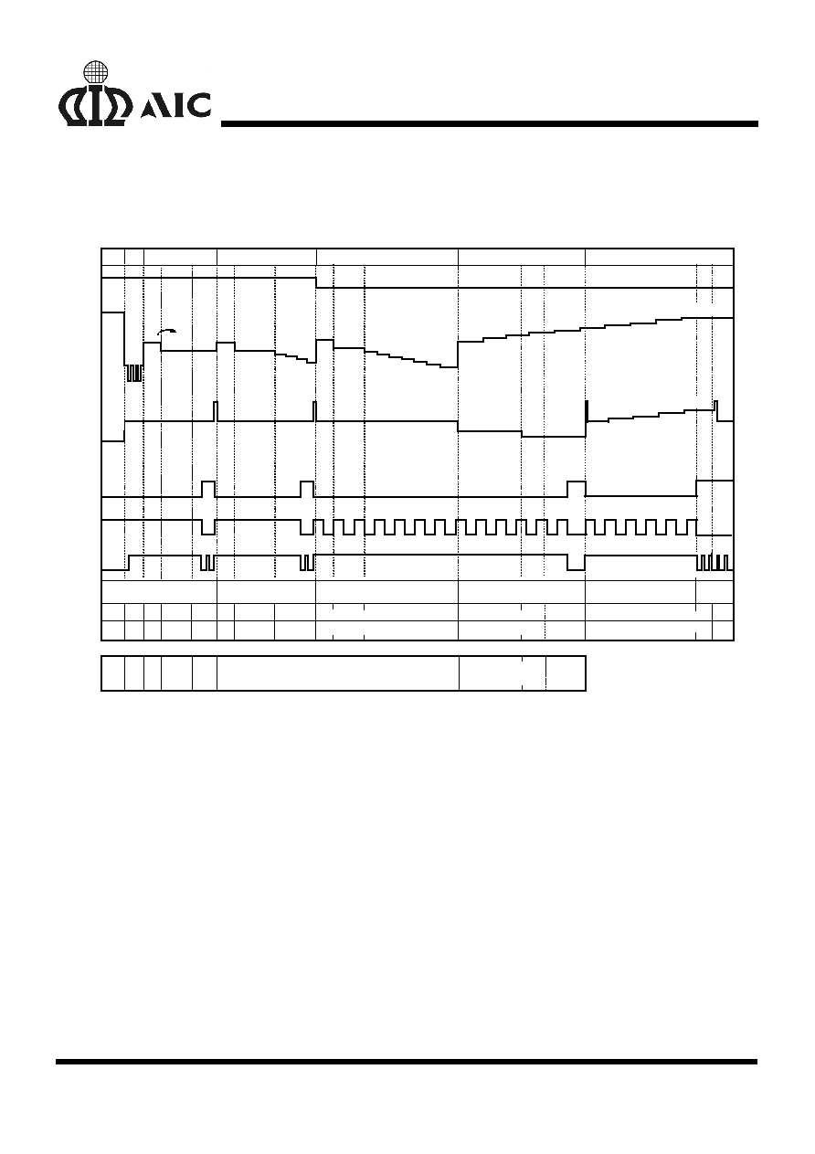
AIC1782
21
TIMING DIAGRAM
0V
SAFETY TIMER TEST
T/t TEST
PEAK TIMER TEST
Power
ON
Init.
GND
GND
GND
Floating
VCC
Floating
Floating
Floating
4V
(-0.15%)
(-0.15%)
(-2.5%)
4V
ON
OFF
4V
2mV
Step/100mS
2mV
Step/100mS
2V
1.993V
(-0.35%)
2V
2V
1.
95
V
ON
1.96V
2V
4V
2V
1.9V
1.997V
1.997V
1.997V
1.5V
(-2.15%)
1.85V
5V
1.12V
ON
ON
OFF
3.2KHz
ON
OFF
ON
OFF
OFF
OFF
OFF
ON
VCC, SEL3, MODE=5V, (DSW FREQ.=820KHz, 25 TIMES of 32.8K)
-
V DISALBE TEST
-
V TEST
1.32
9
0.4
8
0.12
4
0.74
0.12
2
0.02
10
0.32
5
0.32
0.97
0.32
0.26
3
0.24
0.1
0.5
7
0.12
6
5.89
5.99
6.01
4.57
4.17
3.93
3.43
2.46
2.14
1.26
1
2.02
1.17
1.38
0.26
0.14
0.14
1
Floating
GND
Floating
Floating
OFF
ON
<2.1V
<2.1V
2V
2V
0.4
16
Delay 0.3
14
0.74
0.12
12
0.26
13
0.24
0.5
15
8.91
8.51
8.27
7.77
7.47
7.21
(A):ICOA
(B):ICOB
(A):ABV
(B):BBV
ADJ
(A):LEA2
(B):LEB2
(A):LEA1
(B):LEB1
(A):ATS
(B):BTS
TIME (A)
(SEC.)
STAGE
SEL1
SEL2
TIME (B)
(SEC.)
STAGE
0
6.11
6.37
6.25
0.14
11
2V
0.1
6.01
3V
0.1
Fig. 5 Timing Diagram of AIC1782 in Test Mode
AIC1782
22
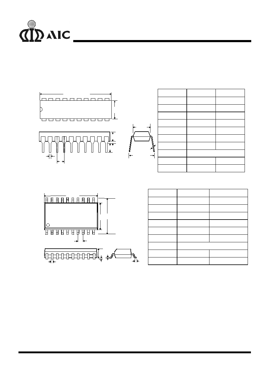
PHYSICAL DIMENSIONS
20 LEAD PLASTIC DIP (unit: mm)
SYMBOL
MIN
MAX
A1
0.381
--
A2
2.92
4.96
b
0.35
0.56
C
0.20
0.36
D
24.89
26.93
E
7.62
8.26
E1
6.09
7.12
e
2.54(TYP)
eB
--
10.92
b
e
L
A1
A
E1
D
eB
E
C
L
2.92
3.81
20 LEAD PLASTIC SO (300 mil) (unit: mm)
SYMBOL
MIN
MAX
A
2.35
2.65
A1
0.10
0.30
B
0.33
0.51
C
0.23
0.32
D
12.60
13.00
E
7.40
7.60
e
1.27(TYP)
H
10.00
10.65
e
B
A
A
1
D
C
E
H
L
L
0.40
1.27