AIC1802
Two-Cell Lithium-Ion Battery Protection IC
DS-1802-03 July 13, 00
www.analog.com.tw
1
n
FEATURES
l
Ultra-Low Quiescent Current at 10
µ
A (V
CC
=7V,
V
C
=3.5V).
l
Ultra-Low Power-Down Current at 0.2
µ
A (V
CC
=3.8V, V
C
=1.9V).
l
Wide Supply Range: 2 to 18V.
l
Precision Overcharge Protection Voltage
4.35V
±
30mV for the AIC1802A
4.30V
±
30mV for the AIC1802B
4.25V
±
30mV for the AIC1802C
l
Built-in Delay Circuits for Overcharge, Over-
discharge and Overcurrent Protection.
l
Overcharge and Overdischarge Delay Time
can be Extended by External Capacitors.
l
Built-in Cell-balancing Bleeding Network under
Overcharge Condition.
n
APPLICATIONS
l
Protection IC for Two-Cell Lithium-Ion Battery
Pack.
n
DESCRIPTION
The AIC1802 battery protection IC is designed
to protect lithium-ion batteries from damage due
to overcharging,
overdischarging, and
overcurrent for two series cells in portable
phones and laptop computers. It can be a part of
the low-cost charge control system within a two-
cell lithium-ion battery pack.
Safe and full utilization charging is ensured by
the accurate
±
30mV overcharge detection.
Three different specification values for
overcharge protection voltage are provided for
various protection requirements. The very low
standby current drains little current from the
cells while in storage.
n
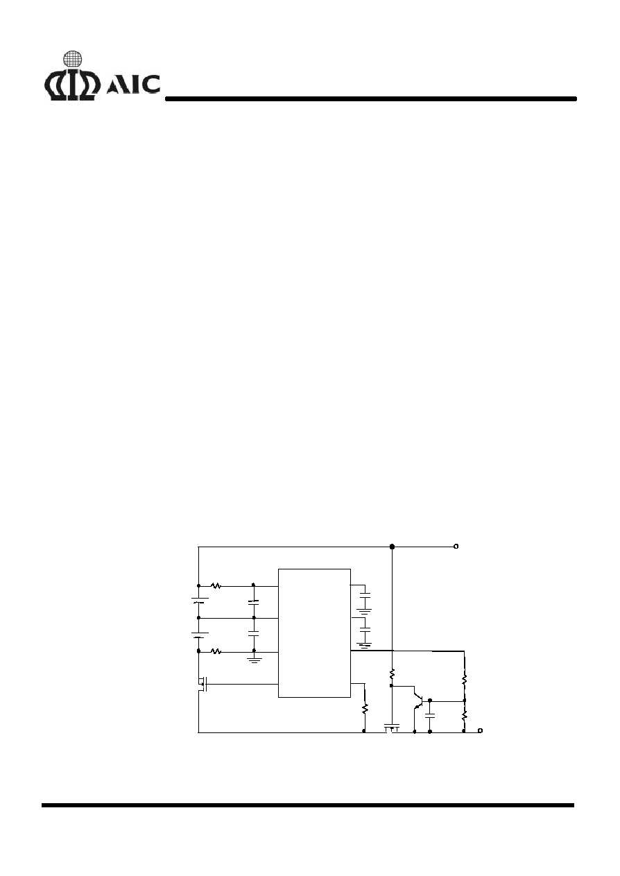
TYPICAL APPLICATION CIRCUIT
5
3
7
4
2
1
6
8
AIC1802
*C
TC
& C
TD
are optional for delay time adjustment.
**R1 & R2: Refer application informations.
C2
1
µ
F
*C
TC
CEM9926
*C
TD
VCC
TC
VC
TD
GND
OC
OD
CS
BATTERY 1
BATTERY 2
M1
CEM9926
C1
1
µ
F
R6
1K
M2
V
BAT
+
V
BAT
-
R4
1M
Q1
R5
1M
R3
1M
**R1
**R2
C3
0.01
µ
F
Protection Circuit for Two-Cell Lithium-Ion Battery Pack

AIC1802
2
n
ORDERING INFORMATION
AIC1802 XCX
PACKAGE TYPE
S: SOP-8
OVERCHARGE
PROTECTION VOLTAGE
A: 4.35V
B: 4.30V
C: 4.25V
ORDER NUMBER
AIC1802ACS
AIC1802BCS
AIC1802CCS
(PLASTIC SO8)
PIN CONFIGURATION
TOP VIEW
VC
VC
OD
TD
GND
CS
TC
OC 1
3
4
2
8
6
5
7
n
ABSOLUTE MAXIMUM RATINGS
Supply Voltage
....................................... ... ... ... ... .....................................................
18V
DC Voltage Applied on VC, CS, OC, OD Pins .................. ... ... ... ... .............................. 18V
DC Voltage Applied on TC, TD Pins .................. ... ... ... ... ... ... ..... ... .............................. 5V
Operating Temperature Range
.......................................... .... ... ... ... .............. -40
∞
C~85
∞
C
Storage Temperature Range ............................ ... ... ... ... ... ... ..................... - 65
∞
C~150
∞
C
n
TEST CIRCUIT
+
+
V
CC
V
C
8
7
6
5
4
3
2
1
AIC1802
OC
VCC
OD
CS
TD
VC
GND
TC
I
C
V
CS
C
TC
V
OD
I
CO
I
CC
C
TD
AIC1802
3
n
ELECTRICAL CHARACTERISTICS
(Ta=25
∞
C, unless otherwise specified.)
PARAMETER
TEST CONDITIONS
SYMBOL
MIN.
TYP.
MAX.
UNIT
Supply Current in Normal Mode
V
CC
=7V, V
C
=3.5V
I
CC
10
15
µ
A
Supply Current in Power-Down
Mode
V
CC
=4.8V, V
C
=2.4V
I
PD
0.8
1.2
µ
A
VC Pin Input Current
V
CC
=7V, V
C
=3.5V
I
C
400
600
nA
AIC1802A
4.32
4.35
4.38
AIC1802B
4.27
4.30
4.33
Overcharge Protection Voltage
AIC1802C
V
OCP
4.22
4.25
4.28
V
Overcharge Release Voltage
V
OCR
3.85
4.0
4.15
V
Overdischarge Protection
Voltage
V
ODP
2.25
2.4
2.55
V
Overdischarge Release Voltage
V
ODR
2.85
3.0
3.15
V
Overcurrent Protection Voltage
V
CC
=7V
V
OIP
135
150
165
mV
Overcharge Delay Time (1)
V
CC
=8.6V, V
C
=4.3V,
C
TC
=0
µ
F
T
OC1
12
25
38
mS
Overcharge Delay Time (2)
V
CC
=8.6V, V
C
=4.3V,
C
TC
=0.47
µ
F
T
OC2
0.7
1.1
1.5
S
Overdischarge Delay Time (1)
V
CC
=4.8V, V
C
=2.4V,
C
TD
=0
µ
F
T
OD1
12
25
38
mS
Overdischarge Delay Time (2)
V
CC
=4.8V, V
C
=2.4V,
C
TD
=0.47
µ
F
T
OD2
0.7
1.1
1.5
S
Overcurrent Delay Time (1)
V
CC
=7V, V
C
=3.5V,
V
CS
=0.15V
T
OI1
4
9
14
mS
Overcurrent Delay Time (2)
V
CC
=7V, V
C
=3.5V,
V
CS
=0.36V
T
OI2
1.0
2.0
3.0
mS
OC Pin Source Current
V
CC
=8.6V, V
C
=4.3V,
OC Pin Short to GND
I
CO
270
400
530
µ
A
OD Pin Output "H" Voltage
V
DL
V
CC
-0.1 V
CC
-0.02
V
AIC1802
4
n
ELECTRICAL CHARACTERISTICS
(Continued)
PARAMETER
TEST CONDITIONS
SYMBOL
MIN.
TYP.
MAX.
UNIT
OD Pin Output "L" Voltage
V
DH
0.01
0.1
V
Charge Detection Threshold
Voltage
V
CC
=4.8V
V
CH
-0.55
-0.4
V
Unbalance Discharge Current
V
CC
=8.3V, V
C
=4V
I
UD
5.4
7.7
10
mA
n
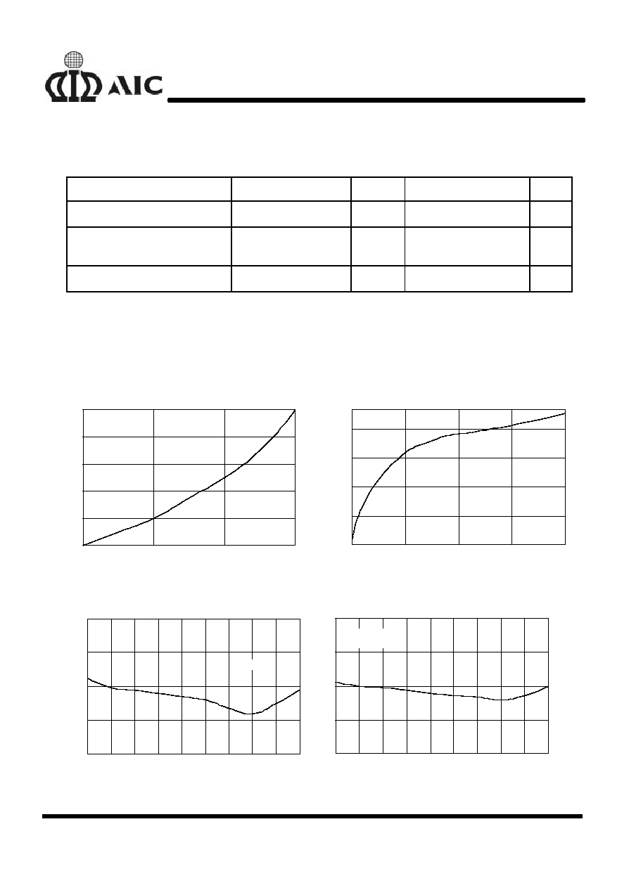
TYPICAL PERFORMANCE CHARACTERISTICS
Supply Current (
µ
A)
Supply Voltage (V)
Supply Current vs. Supply Voltage
5.5
6.5
7.5
8.5
9.7
9.9
10.1
10.3
10.5
10.7
V
C
=1/2V
C C
T
A
=25
∞
C
Power-Down Current (
µ
A)
Supply Voltage (V)
Power-down Current vs. Supply Voltage
V
C
=1/2V
CC
T
A
=25
∞
C
3.8
4.3
4.8
5.3
5.8
0.2
0.35
0.5
0.65
0.8
Overcharge Protection Voltage (V)
Temperature (
∞
C)
Overcharge Protection Voltage vs. Temperature
0
10
20
30
40
50
60
70
-10
-20
4.3
4.305
4.31
4.315
4.32
AIC1802B
Overcurrent Protection Voltage (mV)
Temperature (
∞
C)
Overcurrent Protection Voltage vs. Temperature
0
10
20
30
40
50
60
70
-10
-20
140
142.5
145
147.5
150
V
CC
=7V
V
C
=3.5V
AIC1802
5
n
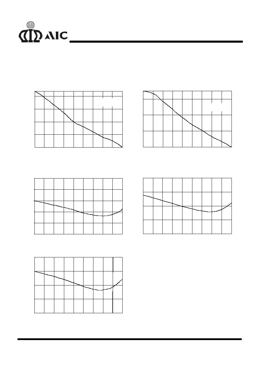
TYPICAL PERFORMANCE CHARACTERISTICS
(Continued)
Supply Current (
µ
A)
Temperature (
∞
C)
Supply Current vs. Temperature
0
10
20
30
40
50
60
70
-10
-20
8.5
9.5
10.5
11.5
12.5
V
CC
=7V
V
C
=3.5V
Power-Down Current (
µ
A)
Temperature (
∞
C)
Power-Down Current vs. Temperature
0
10
20
30
40
50
60
70
-10
-20
0.5
0.7
0.9
1.1
V
CC
=4.8V
V
C
=2.4V
Temperature (
∞
C)
-20
-10
0
10
20
30
40
50
60
70
2.395
2.400
2.405
2.410
2.415
2.420
Overdischarge Protection Voltage vs. Temperature
Overdischarge Protection Voltage
(V)
Overcharge Release Voltage vs. Temperature
Overcharge Release Voltage (V)
Temperature (
∞
C)
-20
-10
0
10
20
30
40
50
6 0
7 0
4.005
4.010
4.015
4.020
4.025
Temperature (
∞
C)
70
Overdischarge Release Voltage vs. Temperature
-20
-10
0
10
20
30
40
50
60
70
3.005
3.010
3.015
3.020
3.025
Overdischarge Release Voltage (V)
AIC1802
6
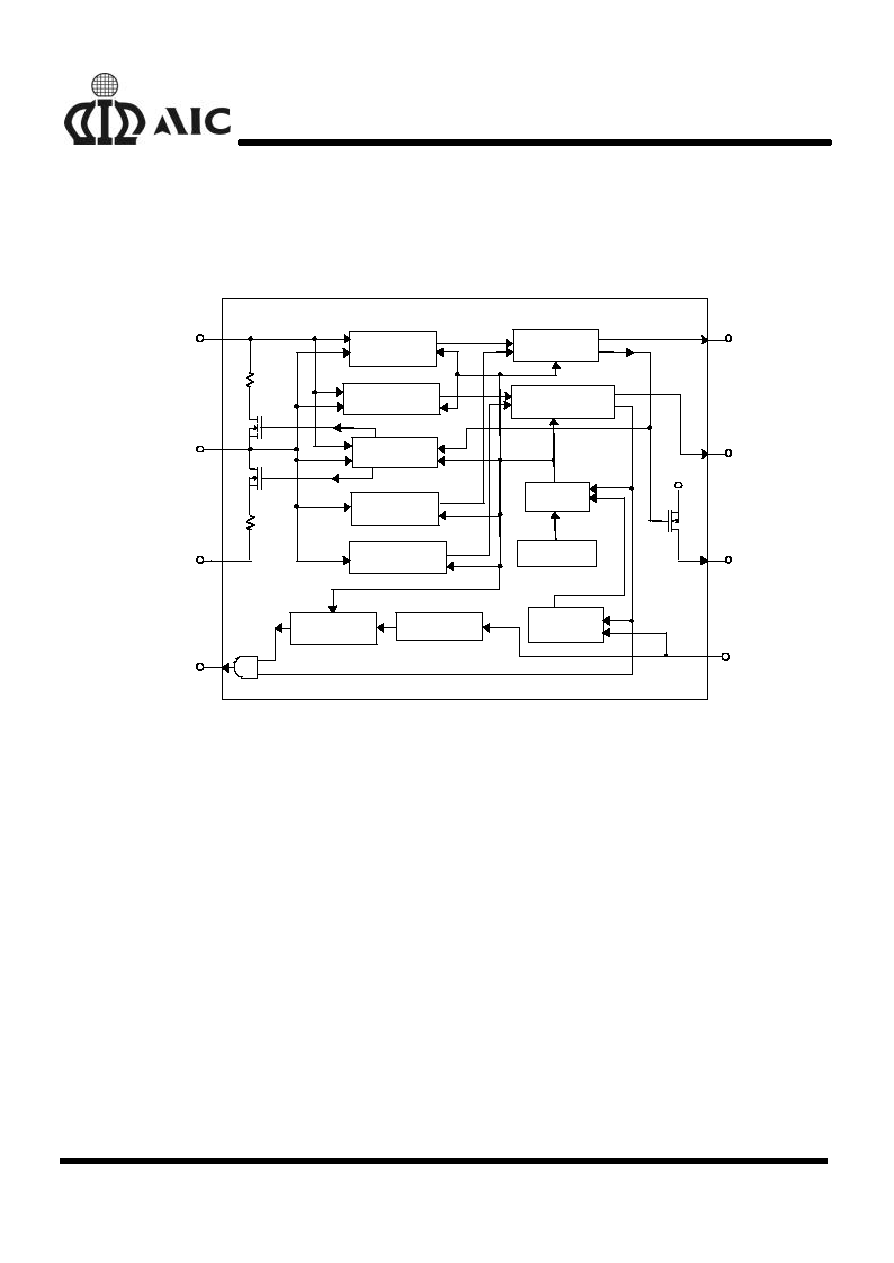
n
BLOCK DIAGRAM
5
3
7
1
6
8
2
4
VCC
TC
TD
OC
CS
OD
VC
GND
VCC
450
450
OVERCURRENT
DELAY CIRCUIT
OVERCURRENT
DETECTOR
CHARGE
DETECTION
OVERDISCHARGE
DETECTOR 2
TIMING
GENERATION
OVERCHARGE
DETECTOR 1
OVERCHARGE
DELAY CIRCUIT
OVERDISCHARGE
DETECTOR 1
OVERDISCHARGE
DELAY CIRCUIT
OVERCHARGE
DETECTOR 2
LOGIC
CONTROL
WAKE-
UP
POWER-
DOWN
UNBALANCE
DISCHARGE
n
PIN DESCRIPTIONS
PIN 1: OC
- PMOS open drain output for
control of the charge control
MOSFET M2. When overcharge
occurs, this pin sources current to
switch the external NPN Q1 on,
and charging is inhibited by
turning off the charge control
MOSFET M2.
PIN 2: OD
- Output pin for control of the
discharge control MOSFET M1.
When overdischarge occurs, this
pin goes low to turn off the
discharge control MOSFET M1
and discharging is inhibited.
PIN 3: TD
- Overdischarge delay time setting
pin.
PIN 4: GND - Ground pin. This pin is to be
connected to the negative terminal
of the lower battery cell.
PIN 5: TC
- Overcharge delay time setting
pin.
PIN 6: VC
- To be connected to the positive
terminal of the lower cell and
the negative terminal of the
upper cell.
PIN 7: CS
- Input pin for current sensing.
Using the drain-source voltage
of the discharge control
MOSFET M1 (voltage between
CS and GND), it senses
discharge current during normal
mode and detects whether
charging current is present
during power down mode.
PIN 8: VCC - Power supply pin. It is to be
connected to the positive
terminal of the upper cell.

AIC1802
7
n
APPLICATION INFORMATIONS
THE OPERATION
Overcharge Protection
When the voltage of either of the battery cells
exceeds V
OCP
(overcharge protection voltage)
beyond the overcharge delay time period,
charging is inhibited by the turning-off of the
charge control MOSFET M2. The overcharge
delay time (T
OC
) defaults to 25mS and can be
extended by adding a capacitor C
TC
. Inhibition of
charging is immediately released when the
voltage of the overcharged cell becomes lower
than V
OCR
(overcharge release voltage) through
discharge.
Overdischarge Protection
When the voltage of either of the battery cells
goes below V
ODP
(overdischarge protection
voltage) beyond the overdischarge delay time
period, discharging is inhibited by the turning-off
of the discharge control MOSFET M1. The
overdischarge delay time (T
OD
) defaults to 25mS
and can be extended by adding a capacitor C
TD
.
Inhibition of discharging is immediately released
when the voltage of the overdischarged cell
becomes higher than V
ODR
(overdischarge
release voltage) through charging.
Power-Down after Overdischarge
When overdischarge occurs, the AIC1802 will go
into power-down mode, turning off all the timing
generation and detection circuitry to reduce the
quiescent current to 0.8
µ
A (V
CC
=4.8V). In the
unusual case where one battery cell is
overdischarged while the other under overcharge
condition, the AIC1802 will turn off all the
detection circuits except the overcharge detection
circuit for the cell under overcharge condition.
Charge Detection after Overdischarge
When overcharge occurs, the discharge control
MOSFET M1 turns off and discharging is inhibited.
However, charging is still permitted through the
parasitic diode of M1. Once the charger is
connected to the battery pack, the AIC1802
immediately turns on all the timing generation and
detection circuitry and goes into normal mode.
Charging is determined to be in progress if the
voltage between CS and GND is below ≠0.4V
(charge detection threshold voltage V
CH
)
Overcurrent Protection
In normal mode, the AIC1802 continuously
monitors the discharge current by sensing the
voltage of CS pin. If the voltage of CS pin
exceeds V
OIP
(overcurrent protection voltage)
beyond overcurrent delay time T
OI
period, the
overcurrent protection circuit operates and
discharging is inhibited by turning-off of the
discharge control MOSFET M1. Discharging must
be inhibited for at least 256mS after overcurrent
takes place to avoid damage to external control
MOSFETs due to rapidly switching transient
between V
BAT+
and V
BAT-
terminals. The
overcurrent condition returns to the normal mode
when the load is released and the impedance
between the V
BAT+
and V
BAT-
terminals is 10M
or
higher. For the sake of protection of the external
MOSFETs, the larger the CS pin voltage (which
means the larger discharge current) the shorter
the overcurrent delay time. The relationship
between voltage of CS pin and overcurrent delay
AIC1802
8
time T
OI
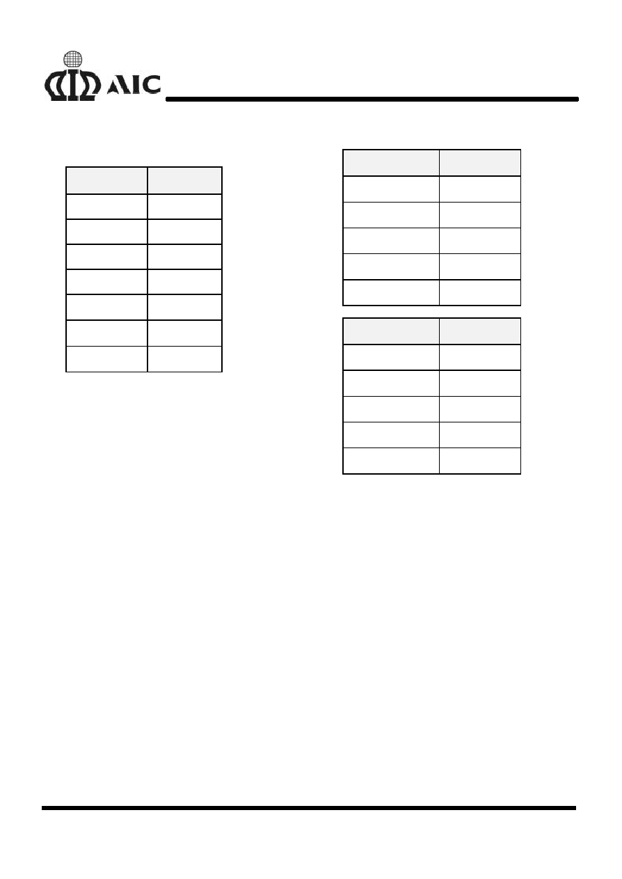
is tabulated as below.
V
CS
(V)
T
OI
(S)
150m
9.0m
200m
5.6m
300m
2.8m
360m
2.0m
1V
540
µ
3V
290
µ
5V
270
µ
Unbalanced Discharge after Overcharge
When either of the battery cells is overcharged,
the AIC1802 will automatically discharge the
overcharged cell at about 7.7mA until the voltage
of the overcharged cell is equal to the voltage of
the other cell. If the voltage of the other cell is
below V
OCR
, the internal cell-balance "bleeding"
will proceed until the voltage of the overcharged
cell decreases to V
OCR
.
DESIGN GUIDE
Adjustment of Overcharge and
Overdischarge Delay Time
Both the overcharge and overdischarge delay
times default to 25mS and can be extended by
adding the external capacitors C
TC
and C
TD
,
respectively. Increasing the capacitance value will
increase the delay time. The relationship between
capacitance of the external capacitors and delay
time is tabulated as below:
C
TC
(F)
T
OC
(S)
0
µ
25m
0.1
µ
320m
0.3
µ
890m
0.47
µ
1.12
0.57
µ
1.43
C
TD
(F)
T
OD
(S)
0
µ
25m
0.1
µ
320m
0.3
µ
820m
0.47
µ
1.08
0.57
µ
1.39
Selection of External Control MOSFETs
Because the overcurrent protection voltage is
preset, the threshold current for overcurrent
detection is determined by the turn-on resistance
of the discharge control MOSFET M1. The turn-
on resistance of the external control MOSFETs
can be determined by the equation: R
ON
=V
OIP
/I
T
(I
T
is the overcurrent threshold current). For
example, if the overcurrent threshold current I
T
is
designed to be 5A, the turn-on resistance of the
external control MOSFETs must be 30m
. Users
should be aware that turn-on resistance of the
MOSFET changes with temperature variation due
to heat dissipation. It changes with the voltage
between gate and source as well. (Turn-on
resistance of a MOSFET increases as the voltage
between gate and source decreases). Once the
turn-on resistance of the external MOSFET

AIC1802
9
changes, the overcurrent threshold current will
change accordingly.
Suppressing the Ripple and Disturbance
from Charger
To suppress the ripple and disturbance from
charger, connecting C1 to cell 1 and C2 to cell 2 is
necessary.
Controlling the Charge Control
MOSFET
R3, R4, R5 and NPN transistor Q1 are used to
switch the charge control MOSFET M2. If
overcharge does not occur, no current flows out
from OC pin and Q1 are turned off, then M2 is
turned on. When overcharge occurs, current flows
out from OC pin and Q1 is turned on, which turns
off M2 in turn. High resistance for R3, R4, and R5
is recommended for reducing loading of the
batteries.
Latch-Up Protraction at CS Pin
R6 is used for latch-up protection when charger is
connected under overdischarge condition, and
also for overstress protection when charger is
connected in reverse. The charge detection
function after overdischarge is possibly disabled
by larger value of R6. Resistance of 1K
is
recommended.
Selection of R1 and R 2
R1 and R2 are used to avoid large current flow
through the battery pack under the situation of IC
damage or pin short. On the other hand,
resistance of R1 and R2 will affect overcharge
release voltage and bleeding function. The
relationship among Vrelease1,Vrelease2, R1, and
R2 is shown as following equations:
Vrelease1=V
OCR
+I
UD
*R1
Vrelease2=V
OCR
+I
UD
*R2
where
Vrelease1 is Battery 1, real overcharge release
voltage
Vrelease2 is Battery 2, real overcharge release
voltage
Therefore, resistance of R1 and R2 should not
higher than 30
. Otherwise, overcharge release
voltage would be higher than overcharge
protection voltage and the charging current may
oscillate. In addition, if overcharge protection
function occurs, AIC1802 will discharge the
overcharged cell and will stop bleeding function
even if the voltage is not equal to the other. The
recommended resistance of R1 and R2 is from 20
to 30
.
Effect of C3
C3 has to be applied to the circuit. Because C3
will keep AIC1802 to be charged after
overdischarge occurred. In addition, when the
differential voltage between charger and battery
pack is higher than 2.1V and overcharge
protection function work, C3 will avoid battery
pack from being charged even if the battery
voltage lower than 4V (To avoid battery pack from
being charged under charger malfunction
situation). The battery pack can be charged again
till remove it from charger.
AIC1802
10
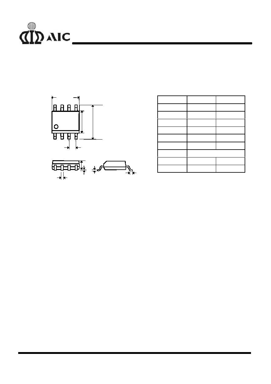
n
PHYSICAL DIMENSIONS
l
8 LEAD PLASTIC SO (unit: mm)
SYMBOL
MIN
MAX
A
1.35
1.75
A1
0.10
0.25
B
0.33
0.51
C
0.19
0.25
D
4.80
5.00
E
3.80
4.00
e
1.27(TYP)
H
5.80
6.20
L
0.40
1.27
D
H
e
A
B
A1
C
E
L