 | –≠–ª–µ–∫—Ç—Ä–æ–Ω–Ω—ã–π –∫–æ–º–ø–æ–Ω–µ–Ω—Ç: AK4356VQ | –°–∫–∞—á–∞—Ç—å:  PDF PDF  ZIP ZIP |
ASAHI KASEI
[AK4356]
M0072-E-01
1999/09
- 1 -
GENERAL DESCRIPTION
The AK4356 is a high performance six channels DAC corresponding to 96kHz sampling mode of DVD.
Two channels of them can operate up to 192kHz sampling fully correspond to DVD-Audio standards. The
AK4356 introduces the advanced multi-bit architecture for
DS
modulator. This new architecture achieves
the wider dynamic range, while keeping much the same superior distortion characteristics as
conventional Single Bit way. In the AK4356, the analog outputs are filtered in the analog domain by
switched-capacitor filter (SCF) with high tolerance to clock jitter. The analog outputs are full differential
output, so the device is suitable for hi-end applications.
FEATURES
o
128x Oversampling
o
Sampling Rate up to 192kHz for 2 channels mode,
96kHz for 6 channels mode
o
24Bit 8 times Digital Filter with Slow roll-off option
Ripple:
±
0.005dB, Attenuation: 75dB
o
THD+N:
-94dB
o
DR, S/N:
112dB
o
High Tolerance to Clock Jitter
o
Low Distortion Differential Output
o
Channel Independent Digital De-emphasis for 32, 44.1 & 48kHz sampling
o
Channel Independent Zero Detect Pin
o
Channel Independent Digital Attenuator with soft-transition
o
Soft Mute
o
3-wire Serial Interface for Volume Control
o
I/F format: MSB justified, LSB justified, I2S
o
TTL Level Digital I/F
o
Master Clock
Normal Speed: 256fs, 384fs, 512fs or 768fs
Double Speed: 128fs, 192fs, 256fs or 384fs
o
Power Supply: 4.75 to 5.25V
o
44pin LQFP Package
o
Ta: -40 to 85
∞
C
192kHz 24Bit Six-Channel DAC for DVD-Audio
AK4356

ASAHI KASEI
[AK4356]
M0072-E-01
1999/09
- 2 -
n
Block Diagram
SCF
DAC
DATT
DZFL1
LOUT1+
LOUT1-
SCF
DAC
DATT
DZFR1
ROUT1+
ROUT1-
SCF
DAC
DATT
DZFL2
LOUT2+
LOUT2-
SCF
DAC
DATT
DZFR2
ROUT2+
ROUT2-
SCF
DAC
DATT
DZFL3
LOUT3+
LOUT3-
SCF
DAC
DATT
DZFR3
ROUT3+
ROUT3-
Audio
I/F
Control
Register
AK4356
MCLK
LRCK
BICK
MCKO
LRCK
BICK
XTI
XTO
Controller
CS
CCLK
CDTI
LRCK
BICK
SDOUT1
SDOUT2
SDOUT3
AC3
SDTI1
SDTI2
SDTI3

ASAHI KASEI
[AK4356]
M0072-E-01
1999/09
- 3 -
n
Ordering Guide
AK4356VQ
-40
~+85∞C
44pin LQFP(0.8mm pitch)
AKD4356
Evaluation Board
n
Pin Layout
LOUT1-
RO
UT
1+
1
LOUT1+
44
2
DZFL2
3
DZFR1
4
DZFL1
5
CAD0
6
CAD1
7
PDN
8
BICK
9
MCLK
10
DVDD
11
RO
UT
1-
43
LO
UT
2+
42
LO
UT
2-
41
RO
UT
2+
40
RO
UT
2-
39
LO
UT
3+
38
LO
UT
3-
37
RO
UT
3+
36
RO
UT
3-
35
AV
S
S
34
D
VSS
12
SD
TI
1
13
SD
TI
2
14
SD
TI
3
15
LRCK
16
SM
U
T
E
17
CCLK
18
CDTI
19
CS
N
20
DFS
0
21
CK
S
0
22
33
32
31
30
29
28
27
26
25
24
23
AVDD
VREFH
DZFR2
DZFL3
DZFR3
DZFE
DIF2
DIF1
DIF0
CKS2
CKS1
AK4356VQ
Top View
ASAHI KASEI
[AK4356]
M0072-E-01
1999/09
- 4 -
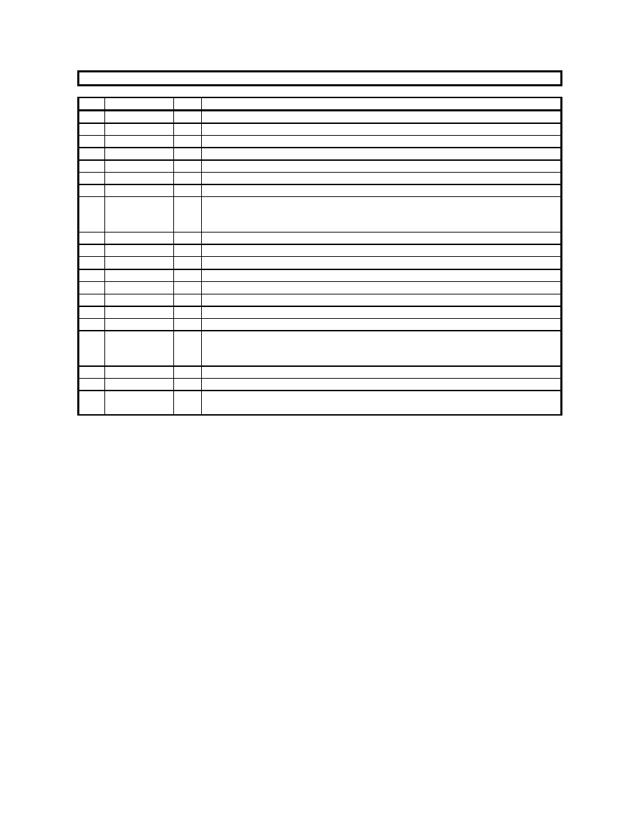
PIN/FUNCTION
No.
Pin Name
I/O
Function
1
LOUT1-
O
DAC1 Lch Negative Analog Output Pin
2
LOUT1+
O
DAC1 Lch Positive Analog Output Pin
3
DZFL2
O
DAC2 Lch Zero Input Detect Pin
4
DZFR1
O
DAC1 Rch Zero Input Detect Pin
5
DZFL1
O
DAC1 Lch Zero Input Detect Pin
6
CAD0
I
Chip Address 0 Pin
7
CAD1
I
Chip Address 1 Pin
8
PDN
I
Power-Down & Reset Pin
When "L", the AK4356 is powered-down and the control registers are reset to
default state. If the state of CAD0-1 changes, then the AK4356 must be reset by PDN.
9
BICK
I
Audio Serial Data Clock Pin
10
MCLK
I
Master Clock Input Pin
11
DVDD
-
Digital Power Supply Pin, +4.75
~+5.25V
12
DVSS
-
Digital Ground Pin
13
SDTI1
I
DAC1 Audio Serial Data Input Pin
14
SDTI2
I
DAC2 Audio Serial Data Input Pin
15
SDTI3
I
DAC3 Audio Serial Data Input Pin
16
LRCK
I
Audio Input Channel Clock Pin
17
SMUTE
I
Soft Mute Pin (Note)
When this pin goes to "H", soft mute cycle is initialized.
When returning to "L", the output mute releases.
18
CCLK
I
Control Data Clock Pin
19
CDTI
I
Control Data Input Pin
20
CSN
I
Chip Select Pin
This pin should be held to "H" except for access.

ASAHI KASEI
[AK4356]
M0072-E-01
1999/09
- 5 -
No.
Pin Name
I/O
Function
21
DFS0
I
Double Speed Sampling Mode 0 Pin (Note)
"L": Normal Speed, "H": Double Speed at DFS1 bit = "0".
22
CKS0
I
Input Clock Select 0 Pin (Note)
23
CKS1
I
Input Clock Select 1 Pin (Note)
24
CKS2
I
Input Clock Select 2 Pin (Note)
25
DIF0
I
Audio Data Interface Format 0 Pin (Note)
26
DIF1
I
Audio Data Interface Format 1 Pin (Note)
27
DIF2
I
Audio Data Interface Format 2 Pin (Note)
28
DZFE
I
Zero Input Detect Enable Pin (Note)
29
DZFR3
O
DAC3 Rch Zero Input Detect Pin
30
DZFL3
O
DAC3 Lch Zero Input Detect Pin
31
DZFR2
O
DAC2 Rch Zero Input Detect Pin
32
VREFH
I
Positive Voltage Reference Input Pin, AVDD
33
AVDD
-
Analog Power Supply Pin
34
AVSS
-
Analog Ground Pin, +4.75
~+5.25V
35
ROUT3-
O
DAC3 Rch Negative Analog Output Pin
36
ROUT3+
O
DAC3 Rch Positive Analog Output Pin
37
LOUT3-
O
DAC3 Lch Negative Analog Output Pin
38
LOUT3+
O
DAC3 Lch Positive Analog Output Pin
39
ROUT2-
O
DAC2 Rch Negative Analog Output Pin
40
ROUT2+
O
DAC2 Rch Positive Analog Output Pin
41
LOUT2-
O
DAC2 Lch Negative Analog Output Pin
42
LOUT2+
O
DAC2 Lch Positive Analog Output Pin
43
ROUT1-
O
DAC1 Rch Negative Analog Output Pin
44
ROUT1+
O
DAC1 Rch Positive Analog Output Pin
Note:SMUTE, DFS0, CKS0, CKS1, CKS2, DIF0, DIF1, DIF2, DZFE pins are ORed with serial control register.