
ASAHI KASEI
[AK4571]
MS0153-J-02
2003/3
- 1 -
:
AK4571 1ch A/D 2ch D/A1
16bit CODECAK4571USB I/FUSB
7
ADCDAC
PLLSIESerial Interface
EngineFIFO
20dB+24dB
-31dB 1dB
D/A
0dB -43dB1dB
AK4571HID
AK4571
AK45711uA
USB
500uA
Microwire EEPROM I/FVendor IDProduct
ID
AK4571
USB
:
n USB
12 Mbps bit rate
USB Serial Interface EngineSIE
Audio Class Processing Block
4 Endpoints
USB transceiver
n 16 bit codec
- A/D Converter
1 channel for Microphone
Pre-Amp (Fixed Gain: 20dB)
Mute/Volume Control
Programmable Gain Control
+24dB to �31dB ( 1dB step )
- D/A Converter
2 channel
- Mixer
Mute/Attenuation Control
+0dB to �47dB ( 1dB step )
Analog Bass Boost
n HID Support
-
-
&
n Power Management
-
n EEPROM Interface (Micrpwore Type)
- Descriptor EEPROM
- 1K/2K/4K bit EEPROM
n On-chip PLL
7
8kHz, 11.025kHz, 16kHz, 22.05kHz,
32kHz, 44.1kHz, 48kHz
n Single Power Supply, Low Power
+3.3Volts
�
0.3V
n Package
48pin LQFP
AK4571
USB I/F Audio CODEC

ASAHI KASEI
[AK4571]
MS0153-J-02
2003/3
- 2 -
MICIN
ATT
ATT
LOUT
ROUT
ADC
DAC
Master
volume
FIFO
Audio
Control
Block
USB
Serial
Interface
Engine
USB
Transceiver
DP
DN
VD
DGND
VA
LFLT_44K
PLL1
MICBIAS
XTLIN
XTLOUT
CRYSTAL
RSTN
AMP1O
AMP2I
AMP2O
LFLT_48K
VCOM VRAD
Config
ROM
String
ROM
Power
Management
DAC
GAIN
EPSW
PLL
GAIN
Mixer
M
M
M
M
VRDA
EPDO
SK
EEPROM I/F
EPEN
EMSW
20dB
EPAI
CS
FIFO
FIFO
EPSEL
VREF
AGND
IMUTE OMUTE DEC
INC
STBY
MSTAT
Bass
Boost
Bass
Boost
RBFI
RBFO
LBFO
LBFI
BGND
LFLT_SYS

ASAHI KASEI
[AK4571]
MS0153-J-02
2003/3
- 3 -
AK4571VQ
0
+70
�
C
48pinLQFP(0.5mm )
AKD4571
AK4571
XTALOUT
VD
DGND
BGND
EPSW
XTALIN
STBY
EMSW
LFLT_SYS
1
10
20
30
40
5
15
25
35
45
MICIN
AMP1O
AMP2I
AMP2O
LBFI
RBFI
RBF
O
ROUT
EPDI
EPAO
SK
CS
TESTMODE2
VRDA
VRAD
AGND
VA
DN
DP
RSTN
SUSN
OMUTE
DEC
INC
MSTAT
MICBIAS
IMUTE
EPSEL
EPEN
LFLT_44K
LFLT_48K
VCOM
LBFO
LOUT
TEST3
TEST1
TEST2
TESTMODE1
TESTMODE3
ASAHI KASEI
[AK4571]
MS0153-J-02
2003/3
- 4 -
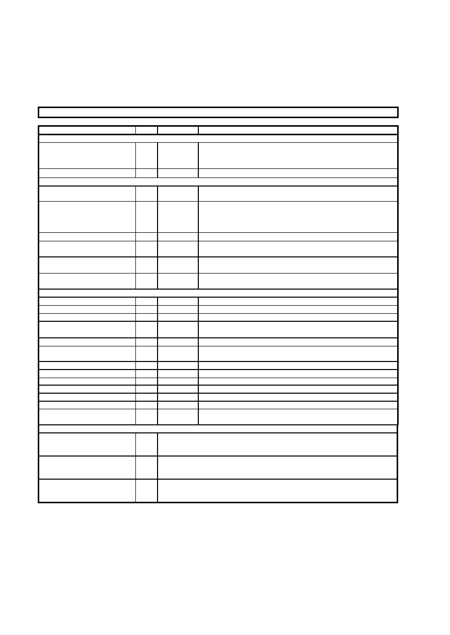
No.
Signal Name
I/O
Ana / Dig
Description
USB Interface
46
DP
I/O
D
USB bus Non-Inverting pin.
Since the AK4571 is a full-speed device, a 1.5k
resistor must be
connected between D+ node to VD.
47
DN
I/O
D
USB bus Inverting Pin.
Reset, Crystal, PLL
45
RSTN
I
D
Reset Pin. Low input resets the chip.
Schmitt Trigger input.
44
SUSN
O
D
Suspend Pin
"L": Suspend Mode
"H": Normal Mode
5
XTALOUT
O
A
Crystal Oscillator Output, Connect Crystal Resonator. Connect capacitor
6
XTALIN
I
A
Crystal Oscillator Input, Connect Crystal Resonator. Connect capacitor
9
LFLT_SYS
O
A
System PLL loop filter Pin. Connect 2.7k
resistor and 22nF capacitor in
series externally.
10
LFLT_44K
O
A
Codec PLL loop filter Pin. Connect 120k
resistor and 6.8nF capacitor in
series externally.
11
LFLT_48K
O
A
Codec PLL loop filter Pin. Connect 120k
resistor and 6.8nF capacitor in
series externally.
Analog Input/Output
12
VCOM
O
A
Analog Common Voltage Reference Pin
27
VRAD
O
A
ADC Common Voltage Reference Pin.
26
VRDA
O
A
ADC Common Voltage Reference Pin.
14
MICIN
I
A
Mono Channel Microphone Input
15
AMP1O
O
A
Mono Channel 1
st
Amplifier Output Pin
16
AMP2I
I
A
Mono Channel 2
nd
Amplifier Input Pin
17
AMP2O
O
A
Mono Channel 2
nd
Amplifier Output Pin
Please Connect 1nF capacitor.
21
LOUT
O
A
Left Channel D/A Out
25
ROUT
O
A
Right Channel D/A Out
19
LBFI
I
A
Left Channel Bass Boost Filter Input Pin
20
LBFO
O
A
Left Channel Bass Boost Filter Output Pin
22
RBFI
I
A
Right Channel Bass Boost Filter Input Pin
23
RBFO
O
A
Right Channel Bass Boost Filter Input Pin
13
MICBIAS
O
A
Voltage Reference Output for the Microphone's bias voltage
When the chip goes into Suspend mode, this pin goes to Hi-Z.
External Headphone Amplifier Control
6
EPSW
O
External Headphone Amplifier Power Switch Control Pin 1
"H": Normal Operation
"L": Suspend Mode
7
STBY
O
External Headphone Amplifier Power Switch Control Pin 2
"L": Normal Operation
"H": Suspend Mode
8
EMSW
O
External Headphone Amplifier Mute Control Pin
"H": MUTE ON
"L": MUTE OFF

ASAHI KASEI
[AK4571]
MS0153-J-02
2003/3
- 5 -
No.
Signal Name
I/O
Ana / Dig
Description
EEPROM I/F
31
CS
O
D
EEPROM I/F Chip Select Pin
32
SK
O
D
Read Clock Pin
34
EPDI
I
D
EEPROM Data Input Pin
33
EPAO
O
D
EEPROM Address Output Pin
35
EPEN
I
D
EEPROM Enable Pin
"H": Read Device/String Descriptor from external EEPROM
"L": Read Device/String Descriptor from internal ROM.
CS,SK,EPDI,EPAO are Hi-Z
36
EPSEL
I
D
EEPROM Select
"L": 1Kbit Type EEPROM is connected.
"H": 2Kbit/4Kbit EEPROM is connected
HID Interface
39
IMUTE
I
D
A/D Mute
Toggles mute status at the rising edge. If this pin is not used, please
connect this pin to DGND.
43
OMUTE
I
D
D/A Mute
Sets "1" to internal register at the rising edge, and reset to "0" at the
falling edge. If this pin is not used, please connect this pin to DGND.
41
INC
I
D
D/A Volume Up Pin
Sets "1" to internal register at the rising edge, and reset to "0" at the
falling edge. If this pin is not used, please connect this pin to DGND.
42
DEC
I
D
D/A Volume Down Pin
Sets "1" to internal register at the rising edge, and reset to "0" at the
falling edge. If this pin is not used, please connect this pin to DGND.
40
MSTAT
O
D
Recording Mute Status Pin.
"H": Mute ON
"L": Mute OFF
In suspend mode, this pin is "L".
Power Supply
25
VA
P
A
Analog Power Supply, 3.3V
26
AGND
P
A
Analog Ground
1
VD
P
D
Digital Power Supply, 3.3V
2
DGND
P
D
Digital Ground
3
BGND
P
D
Bulk Ground, 0V
Test Mode
18
TESTMODE1
I
Please tie down to AGND for normal operation.
29
TESTMODE2
I
Please tie down to AGND for normal operation.
30
TESTMODE3
I
Please tie down to AGND for normal operation.
38
TEST1
I
Please tie down to DGND for normal operation.
37
TEST2
O
Please open state
48
TEST3
I
Please tie down to DGND for normal operation.