 | –≠–ª–µ–∫—Ç—Ä–æ–Ω–Ω—ã–π –∫–æ–º–ø–æ–Ω–µ–Ω—Ç: AK5370 | –°–∫–∞—á–∞—Ç—å:  PDF PDF  ZIP ZIP |

ASAHI KASEI
[AK5370]
MS0027-E-00
1
2000/05
General Description
The AK5370 is AD converter for USB audio, especially
USB microphone . The AK5370 integrates USB serial
interface engine, USB transceiver, audio class decoder,
endpoints, and high quality AD converter into t he chip.
As the AK5370 incorporates PLL, it can support several
sampling frequencies, 8kHz, 11.025kHz, 22.05kHz, 44.1kHz,
and 48kHz with only one crystal. Moreover, the AK5370
integrates volume control, and mute function.
It is possible to make USB microphone with a few external
components
This device is good for not only business application such
as conferencing but also games, voice recognition, and
Karaoke.
Related Documents
For the detail of USB specification, and Audio Class, please
refer to the following documents.
Universal Serial Bus Specification Revision 1.1
Universal Serial Bus Device Class Definition for Audio
Devices, Revision 1.0
Features:
n
Incorporates USB Audio Controller
USB Serial Interface Engine
Audio Class Encoder/Decoder
2 Endpoints (FIFO)
USB transceiver
n
16 bit A/D Converter
1 channel
Mute/Volume Control
AGC pin for external control
A/D S/N: 84dBA (44.1kHz, Gain = 0dB)
n
On-chip PLL
5 Sampling Frequencies support
8kHz, 11.025kHz
22.05kHz, 44.1kHz, 48kHz
n
Programmable Gain Amplifier
+20dB to ≠58dB
n
Single Power Supply, Low Power
+3.3Volts
±
10%
n
Package
24pin VSOP
VA
LFLT1
AMP1O
MIC_IN
EndPoint1
IN_FIFO
AGND
VD
16bit
ADC
DGND
DN
DP
Mute
&
Volume
control
EndPoint0
IN_FIFO
EndPoint0
OUT_FIFO
Common Voltage
Audio Class
Decoder
Audio Class
Encoder
Serial
Interface
Engine
XTLIN
XTLOUT
VCOM
USB
Transceiver
PLL
adCLK
System
CLK
CRYSTAL
AMP2O
AMP2I
-
+
-
+
Power
Management
MIC_BIAS
Config ROM
AGC
RST
AGCEN
String ROM
Testmode1,2
TEST1,2,3
LFLT2
VREF
AK5370
USB I/F A/D Converter

ASAHI KASEI
[AK5370]
MS0027-E-00
2
2000/05
Pin/Function
No.
Signal Name
I/O Ana / Dig
Description
1 DGND
P D
Digital
Ground
2
VD
P
D
Digital Power Supply, 3.3V
3
DP
I/O D
USB bus Non-Inverting pin.
Because AK5370 is full speed mode device, 1.5k
resistor will
be connected between D+ node to VD.
4
DN
I/O D
USB bus Inverting Pin.
5
TESTMODE3
I
D
Please tie down to AGND for normal operation.
6
XTALOUT
O
A
Crystal Oscillator Output, Connect Crystal Resonator
7
XTALIN
I
A
Crystal Oscillator Input, Connect Crystal Resonator
8
TESTMODE2
I
A
Please tie down to AGND for normal operation.
9 LFLT2
O
A
System clock PLL loop filter Pin. Connect 18k
resistor and
6800pF capacitor in series externally.
10 LFLT1
O A
adPLL loop filter Pin. Connect 51k
resistor and 8200pF
capacitor in series externally.
11 VCOM
O
A
Analog Common Voltage Reference Pin
12 MICIN
I A
Microphone
Input
13 AMP1O
O A
1
st
Amplifier Output Pin
14 AMP2I
I A
2
nd
Amplifier Input Pin
15 VA
P
A
Analog Power Supply, 3.3V
16 AGND
P A
Analog
Ground
17 VREF
O
A
ADC Common Voltage Reference Pin.
18 AMP2O
O A
2
nd
Amplifier Output Pin
19 TESTMODE1
I
A
Please tie down to AGND for normal oper ation.
20 MICBIAS
O
A
Voltage Reference Output for the Microphones bias voltage
When this chip goes into Suspend mode, this pin goes to Hi -Z.
21 TEST
I
D
Please tie down to AGND for normal operation.
22 AGCE
I
D
AGC Enable Control Input Pin.
When the external AGC is used, High level should be applied
to this pin. When Low input is applied, AGC configuration
ROM data is set FALSE. Then AGC output is set to Low.
23 AGC
O
D
AGC Control Pin
When the host requests set AGC_CONTROL request, this pin
goes to H.
L level AGCE input prevents this AGC_CONTROL request.
Low level output at SUSPEND. Default output at Reset is
Low.
24 RSTN
I
D
Reset Pin, Low input makes the chip reset sate.
Schmitt Trigger input.

ASAHI KASEI
[AK5370]
MS0027-E-00
3
2000/05
Absolute Maximum Rating
AGND, DGND=0V
Parameter Symbol
Min
Max
Units
Power Supplies
Analog
Digital
|DGND-AGND|
VA
VD
GND
-0.3
-0.3
4.5
4.5
0.3
V
V
V
Input Current (any pins except for supplies)
IIN
-
±
10
mA
Analog Input Voltage
VINA
-0.3
VA+0.3
V
Digital Input Voltage
VIND
-0.3
VD+0.3
V
Ambient Temperature
Ta
0
70
∞
C
Storage Temperature
Tstg
-40
125
∞
C
Note 1. All voltages with respect to ground
Warning: Operation at or beyond these limits may results in permanent damage to the device. N ormal operation is
not guaranteed at these extremes.
Recommended Operating Condition
AGND, DGND=0V
Parameter
Symbol
Min
typ
Max
Units
Power Supplies
Analog
Digital
VA
VD
3.0
3.0
3.3
3.3
3.6
3.6
V
V
All voltages with respect to ground.
* AKM assumes no responsibility for the usage beyond the condition in this datasheet.

ASAHI KASEI
[AK5370]
MS0027-E-00
4
2000/05
Analog Characteristics
Ta=25
∞
C, VA=VD=3.3V, Signal Frequency=1kHz, Sampling Frequency Fs=44.1kHz
Parameter Min
typ
Max
Units
Mono ADC (1 channel)
Resolution
16
bits
S/N (A weight)
(1
st
and 2
nd
MIC amplifier are set to 0dB)
76 84 dBA
S/(N+D) (-0.5dB analog input)
(1
st
and 2
nd
MIC amplifier are set to 0dB)
62 70 dB
MIC Amplifier (2
nd
Stage) <IPGA> Characteristics
Input Voltage
1.6
Vp-p
Gain Control Range
-58
20
dB
Step Size
0
1.0
2.0
dB
Input Impedance @AMP2I pin
20
K
MIC amplifier(1
st
Stage)
Gain range(defined by external resistors)
0
+20
dB
External Feedback Impedance
20
K
MIC Bias
Output Voltage when 4.7K
resistor connected
0.9VA
Vdc
Output Impedance
200
500
Output Current
3
mA
Power Supplies
Analog
Digital
Total
Power Down(Suspend Mode)
10.5
8.5
4.7
30
mA
mA
mA
mA
FILTER CHARACTERISTICS
(Ta=25
∞
C VA, VD =3.0 - 3.6 V ; fs = 44.1 kHz)
Parameter Symbol
Min
typ
Max
Units
A/D Digital Filter
(Decimation LPF)
Passband
+/- 0.2 dB
PB
0
17.64
KHz
Stopband
SB
26.5
KHz
Passband Ripple
PR
+/- 0.2
dB
Stopband Attenuation
SA
68
dB
Group Delay
GD
0.5
ms
A/Ddigital Filter (HPF)
Frequency Response
-3 dB
-0.5 dB
-0.1 dB
FR
6.85
19.2
44.9
Hz
Hz
Hz
ASAHI KASEI
[AK5370]
MS0027-E-00
5
2000/05
Digital DC Characteristics
Ta=0 - 70
∞
C; VD=3.0 - 3.6V; DGND=0V Measurement under static state
All digital pins except DP, DN. Schmitt hysteresis level of RST pin and levels of all test pins will not be tested.
Parameter Symbol
Min
Typ
Max
Units
AGCE pin H level input voltage
VIH
70%VA
V
AGCE pin L level input voltage
VIL
30%VA
V
RSTN pin H level voltage
VIHR
2.0
V
RSTN pin L level voltage
VILR
0.8
V
H level output voltage IOH= 2mA
VOH
2.4
V
L level output voltage IOL= -2mA
VOL
0.6
V
Input Leakage Current
Iin
±
10
µ
A
Switching Characteristics
Ta=25
∞
C, VA=VD=3.3V
Parameter Symbol
Min
Typ
Max
Units
Master Clock Frequency
MCLK
-
11.2896
-
MHz
Reset input width @RSTN pin(low active)
Wrst
1.0
us
Singe Ended Receiver Threshold
Vse 0.8 2.0 V
Main Clock Stable Time
Vse(max) of D+ to stabilized MCLK
( Xtal oscillator start up + PLL lock -in )
Tostb 100
ms
Reset Signal Recognition
Both D+ and D- < Vse(min) to Reset mode
Trst_rec
2.5 5.5
µ
s
Device Ready
Ready for transaction after reset
Tdrr 10
ms
Suspend Recognition
Idle state ( D+ > Vse(max) & D- < Vse(min) )
to Suspend mode
Tsus_rec 3.0
ms
Resume Time
First flip of D+/D- from Idle sate
To Device Ready*)
Tresm 30
ms
Device Ready: VREF, Xtal oscillator, and PLL get stable and bus trans action with normal rate is ready.
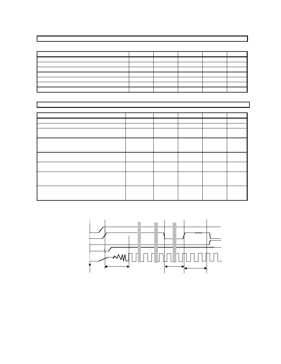
Master
Clock
D- "L"
D+
VD
T
rst_rec
Reset Mode
Device
Connected
RST
Reset Mode
Tostb
Tdrr
Figure 1. Mode change with respect to BUS States 1 (Power on and device connected)