1
ASAHI KASEI
MS0103-E-00
MS0103-E-00
[AK5371]
2001/06
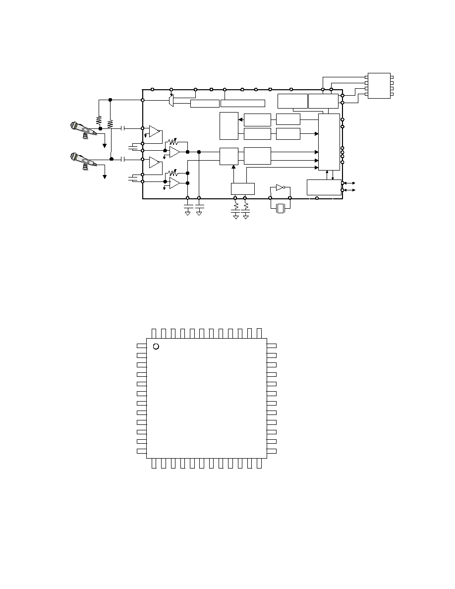
General Description
The AK5371 is stereo A/D converter with USB I/F. The
AK5371 integrates USB serial interface engine, USB
transceiver, audio class processing unit, endpoints, and high
quality 2 channel AD converter into the chip.
As the AK5371 incorporates PLL, it can support several
sampling frequencies, 8kHz, 11.025kHz, 22.05kHz, 44.1kHz,
and 48kHz with only one crystal. Moreover, the AK5371
integrates volume control, and mute function.
Not only power consumption at normal operation is very
low, but also the current at suspend mode is less than 1
µ
A.
The AK5371 includes 20dB fixed gain pre-amplifier. In
addition to this, as the AK5371 also incorporates IPGA which
can amplify the microphone signal up to +24dB, total gain is
44dB maximum.
The AK5371 has EEPROM I/F for customizing Device
Descriptor and String Descriptor. By connecting 1K bit, 2K
bit, or 4Kbit Microwire
TM
type EEPROM, the AK5371 can
customize Vendor ID, Product ID in Device Descriptor, and
String Descriptor.
This device is good for not only business application such as
conferencing but also games, voice recognition, and Karaoke.
Related Documents
For the detail of USB specification, and Audio Class, please
refer to the following documents.
Universal Serial Bus Specification Revision 1.1
Universal Serial Bus Device Class Definition for Audio
Devices, Revision 1.0
Features:
USB-IF Certified
Incorporates USB Audio Controller
USB Serial Interface Engine
Audio Class Encoder/Decoder
2 Endpoints (FIFO)
USB transceiver
16 bit A/D Converter
2 channels
Mute/Volume Control
A/D S/N: 84dBA (44.1kHz, Gain = 0dB)
Low Power Dissipation
Normal Operation: 26mA
Suspend Mode: < 1uA
Programmable Gain Amplifier (IPGA)
+24dB to ≠31dB @1dB Step
20dB Pre-amplifier
On-chip PLL
5 Sampling Frequencies support
8kHz, 11.025kHz
22.05kHz, 44.1kHz, 48kHz
EEPROM I/F
can customize Device Descriptor,
and String Descriptor
Single Power Supply, Low Power
+3.3
±
0.3 Volts
Package
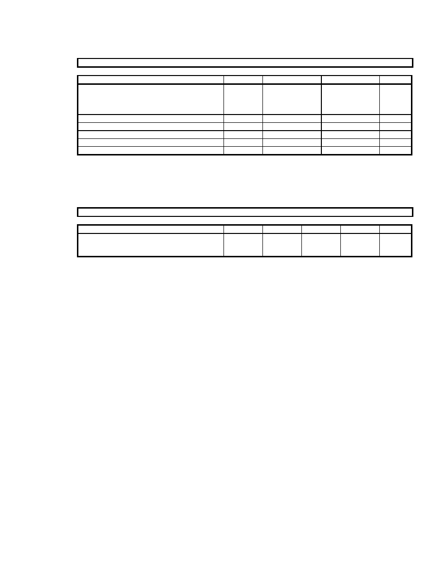
48pin LQFP
AK5371
2ch A/D Converter with USB I/F

3
MS0103-E-00
MS0103-E-00
ASAHI KASEI
[AK5371]
2001/06
Pin/Function
No.
Signal Name
I/O
Ana / Dig
Description
1
VD
P
D
Digital Power Supply, 3.3V
2
DGND
P
D
Digital Ground,0V
3
BGND
P
D
Bulk Ground, 0V
4
NC
-
-
No Connection
5
TESTMODE3
I
D
Please tie down to AGND for normal operation.
6
XTALOUT
O
A
Crystal Oscillator Output, Connect Crystal Resonator
7
XTALIN
I
A
Crystal Oscillator Input, Connect Crystal Resonator
8
TESTMODE2
I
A
Please tie down to AGND for normal operation.
9
LFLT1
O
A
adPLL loop filter Pin. Connect 51k
resistor and 8200pF
capacitor in series externally.
10
LFLT2
O
A
System clock PLL loop filter Pin. Connect 18k
resistor and
6800pF capacitor in series externally.
11
BIASSEL
I
D
MIC BIAS Select Pin
Select MICBIAS Output
"L": VA(through switch)
"H": VREF buffer output
12
NC
-
-
No Connection
13
NC
-
-
No Connection
14
VCOM
O
A
Analog Common Voltage Reference Pin
15
MICBIAS
O
A
Voltage Reference Output for the Microphone's bias voltage
When this chip goes into Suspend mode, this pin goes to Hi-Z.
16
MICL
I
A
Left Channel Microphone Input
17
AMPL1O
O
A
Left Channel 1
st
Amplifier Output Pin
18
AMPL2I
I
A
Left Channel 2
nd
Amplifier Input Pin
19
AMPL2O
O
A
Left Channel 2
nd
Amplifier Output Pin
20
NC
-
-
No Connection
21
MICR
I
A
Right Channel Microphone Input
22
AMPR1O
O
A
Right Channel 1
st
Amplifier Output Pin
23
AMPR2I
I
A
Right Channel 2
nd
Amplifier Input Pin
24
AMPR2O
O
A
Right Channel 2
nd
Amplifier Output Pin

4
MS0103-E-00
MS0103-E-00
ASAHI KASEI
[AK5371]
2001/06
No.
Signal Name
I/O
Ana / Dig
Description
25
NC
-
-
No Connection
26
VA
P
A
Analog Power Supply, 3.3V
27
AGND
P
A
Analog Ground,0V
28
VREF
O
A
ADC Common Voltage Reference Pin.
29
NC
-
-
No Connection
30
TESTMODE1
I
A
Please tie down to AGND for normal operation.
31
NC
-
-
No Connection
32
TEST
I/O
D
Please tie down to AGND for normal operation.
33
CS
O
D
EEPROM I/F Chip Select Pin
34
SK
O
D
Serial Clock Pin
35
EPAO
O
D
EEPROM Address Output Pin
36
NC
-
-
No Connection
37
NC
-
-
No Connection
38
EPDI
I
D
EEPROM Data Input Pin (This pin is internally pulled down)
39
EPEN
I
D
EEPROM Enable Pin
"H" : Read Device Descriptor, String Descriptor from EEPROM
"L" : Read Device/String Descriptor from internal ROM.
Note that CS,SK,EPDI,EPAO is Hi-Z when EPEN is "L"
40
EPSEL
I
D
EEPROM Select Pin
"L" : 1Kbit Type EEPROM is connected.
"H" : 2Kbit/4Kbit EEPROM is connected
If EEPROM is not used, EPSEL should be tied to DGND.
41
NC
-
-
No Connection
42
SUSN
O
D
Suspend Status Pin
"L" : Suspend State
"H" : Normal Operation
43
RSTN
I
D
Reset Pin, Low input makes the chip reset sate.
Schmitt Trigger input.
44
NC
-
-
No Connection
45
NC
-
-
No Connection
46
DP
I/O
D
USB bus Non-Inverting pin.
Because AK5371 is full speed mode device, 1.5k
resistor will
be connected between D+ node to VD.
47
DN
I/O
D
USB bus Inverting Pin.
48
NC
-
-
No Connection
5
MS0103-E-00
MS0103-E-00
ASAHI KASEI
[AK5371]
2001/06
Absolute Maximum Rating
AGND, DGND=0V
Parameter
Symbol
Min
Max
Units
Power Supplies
Analog
Digital
|DGND-AGND|
VA
VD
GND
-0.3
-0.3
4.5
4.5
0.3
V
V
V
Input Current (any pins except for supplies)
IIN
-
±
10
mA
Analog Input Voltage
VINA
-0.3
VA+0.3
V
Digital Input Voltage
VIND
-0.3
VD+0.3
V
Ambient Temperature
Ta
0
70
∞
C
Storage Temperature
Tstg
-40
125
∞
C
Note 1. All voltages with respect to ground
Warning: Operation at or beyond these limits may results in permanent damage to the device. Normal operation
is not guaranteed at these extremes.
Recommended Operating Condition
AGND, DGND=0V
Parameter
Symbol
Min
typ
Max
Units
Power Supplies
Analog
Digital
VA
VD
3.0
3.0
3.3
3.3
3.6
3.6
V
V
All voltages with respect to ground.
* AKM assumes no responsibility for the usage beyond the condition in this datasheet.