 | –≠–ª–µ–∫—Ç—Ä–æ–Ω–Ω—ã–π –∫–æ–º–ø–æ–Ω–µ–Ω—Ç: AK6514CF | –°–∫–∞—á–∞—Ç—å:  PDF PDF  ZIP ZIP |

ASAHI KASEI
[AK6514C]
DAP04E-00
2005/03
- 1 -
AK6514C
SPI bus 64Kbit Serial CMOS EEPROM
Features
Advanced CMOS EEPROM Technology
Single Voltage Supply: 1.8V to 5.5V
128Kbits; 16384 x 8 organization
SPI Serial Interface Compatible
Low Power Consumption
0.8
µ
A Max. (Standby mode)
High Reliability
Endurance:
1000K E/W cycles / Address
Data Retention: 10 Years
Special Features
64 byte Page Write Mode
Block Write Protection (Protect 1/4,1/2 or Entire Array)
Automatic write cycle time-out with auto-ERASE
Software and Hardware controlled Write Protection
Self timed Programming Cycle: 5msec. Max.
Ideal for Low Density Data Storage
Low cost, space saving, 8-pin SOP/ 20-pin QFN package
Block Diagram
128Kbit
16384
◊
8
DATA
REGISTER
INSTRUCTION
DECODE,
CONTROL
AND
CLOCK
GENERATION
INSTRUCTION
REGISTER
EEPROM
SI
CS
SCK
HOLD
ADD.
BUFFERS
VREF
VPP
GENERATOR
VPP SW
DECODER
R/W AMPS
AND
AUTO ERASE
SO
STATUS REGISTER
WP
ASAHI KASEI
[AK6514C]
DAP04E-00
2005/03
- 2 -
General Description
The AK6514C is a 131072-bit, serial, read/write, non-volatile memory device fabricated using an
advanced CMOS EEPROM technology. The AK6514C has 131072-bits of memory organized as
16384 registers of 8 bits each. The AK6514C can operate all function under wide operating
voltage range: 1.8V to 5.5V. The charge up circuit for high voltage generation needed for write
operations is integrated.
The AK6514C serial interface is compatible to a SPI bus. The AK6514C has 6 instructions: READ,
WRITE, WREN (write enable), WRDI (write disable), RDSR (read status register), and WRSR (write
status register).
Each instruction is organized by an op-code (8bits), address (16bits), and data (8bits). When input
level of CS pin changed from high level to low level, AK6514C can receive instructions.
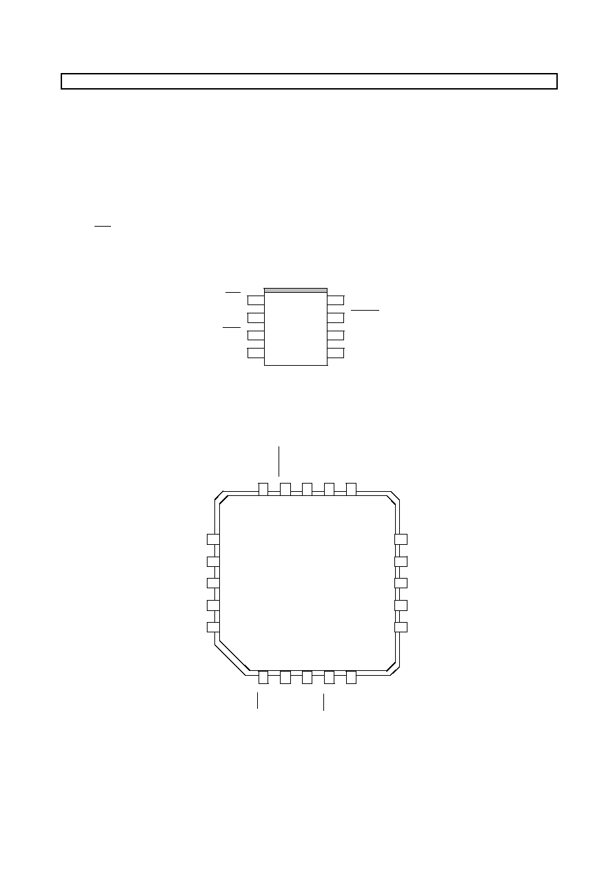
Pin Configurations
AK6514CF
8pin SOP
GND
WP
CS
SO
2
1
3
4
VCC
7
8
6
5
SI
SCK
HOLD
NC
NC
NC
NC
NC
NC
NC
NC
NC
NC
CS
SO
NC
WP
G
ND
V
CC
HO
L
D
NC
SC
K
SI
AK6514CN
5
20
16
10
6
11
15
1
20pin QFN
2
3
4
7
8
9
12
13
14
17
18
19
ASAHI KASEI
[AK6514C]
DAP04E-00
2005/03
- 3 -
Pin name
Functions
CS Chip
Select
input
SCK
Serial Clock input
SI
Serial Data input
SO
Serial Data output
WP
Write Protect input
HOLD Hold
input
VCC Power
Supply
GND Ground
NC
Not Connected *1
*1: Please Open NC pin.
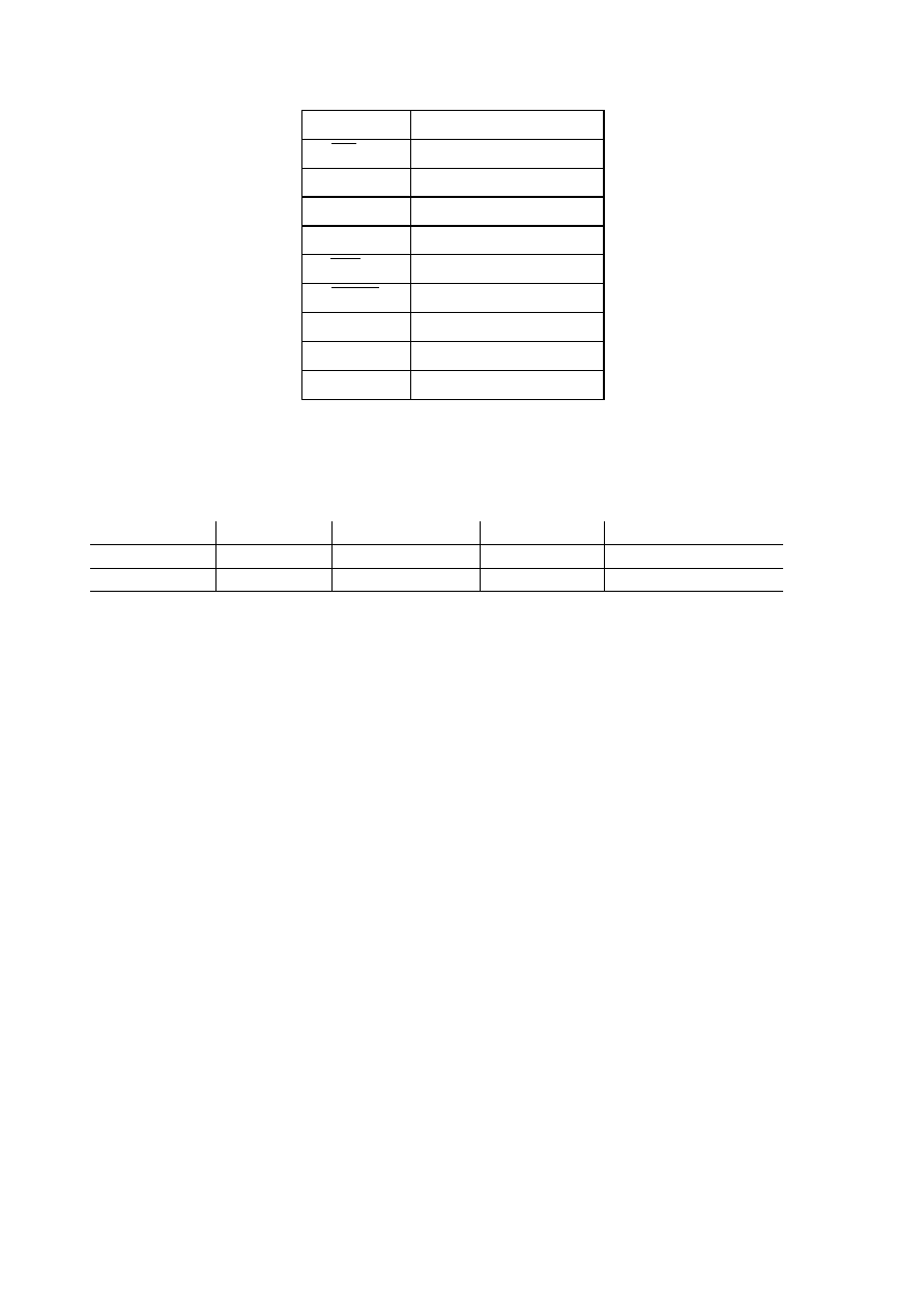
Type of Products
Model
Memory size
Temp. Range
VCC
Package
AK6514CF 128K
bits
-40∞C to +85∞C
1.8V to 5.5V
8pin Plastic SOP
AK6514CN 128K
bits
-40∞C to +85∞C
1.8V to 5.5V
20pin Plastic QFN

ASAHI KASEI
[AK6514C]
DAP04E-00
2005/03
- 4 -
Data Transfer
An IC that outputs the clock is called "MASTER", an IC that receives the clock is called "SLAVE".
The AK6514C operates as a SLAVE. Data is written to the SI pin and read from SO pin. The
MSB is transmitted first.
After CS pin changes hi level to low level, AK6514C receives the first data bit on the SI pin
synchronously with the rising edge of the input pulse of serial clock. While CS pin is high level, the
data input to the SI pin is don't care and SO pin indicates Hi-Z.
All the functions are organized 8 bits of op-code, address, and data. If there is an invalid op-code,
the AK6514C ignores the address and data information and SO pin indicates Hi-Z. In order to input
new op-code, CS pin should be toggled.
Hold
AK6514C has a HOLD pin that can hold the data transfer. When HOLD changes high to low while
SCK is low, the data transfer stops. After the HOLD pin changes high to low while SCK is low, the
data transfer starts again. While the data transfer is paused, AK6514C ignores the clock on the
SCK line.
Write Protect
AK6514C has status registers. When the WPEN bit in the status registers is "1", Write Protect
function is enabled. When WPEN bit is "1" and WP pin is low level, the status register is protected
from write function. When WP pin becomes low level while the WRITE to the status register
instruction is written, the AK6514C doesn't accept the instruction. When the WP pin changes low
level while the internal programming, the programming function continues.
When the WPEN bit is "0", WP pin function is disabled. Even if WP pin is fixed to low level, the
WRITE function to the status register can be done. When the WP pin is high level, AK6514C can
accept all of READ and WRITE functions.

ASAHI KASEI
[AK6514C]
DAP04E-00
2005/03
- 5 -
Pin Description
CS
(Chip Select Input)
When CS changes high level to low level, the AK6514C can receive the instructions.
CS should be kept low level while receiving op-code, address and data, and while outputting
data.
When CS is high level, SO indicate Hi-Z.
SCK
(Serial Clock Input)
The SCK clock pin is the synchronous clock input for input/output data.
SI
(Serial Data Input)
The op-code, address, and data are written to the SI pin.
SO
(Serial Data Output)
The SO pin outputs the data from memory array and status register.
WP
(Write Protect Input)
The WP pin controls the write function to the status register.
When the WPEN bit in the status register is "0", the function of WP pin becomes disable.
Then the status register can be programmable when the WEN bit in the status register is "1".
And it does not depend on the status of WP pin.
When the WPEN bit is "1", the function of WP is enabled. Then the status register can not
be programmable when the WEN bit is "1" and the status of WP pin is low.
When the WPEN bit is "1", WP pin is high and WEN bit is "1", AK6514C can accept the
WRITE instruction to the status registers.
During the instruction input, WP pin should keep high or low level.
HOLD
(Hold Input)
The HOLD pin can hold the data transfer. When the HOLD pin changes hi to low while the
SCK is low, the data transfer is held. And the transfer starts when the HOLD pin changes
low to high while the SCK is low. While the holding the data transfer, AK6514C ignores the
clock signal on SCK pin.