ASAHI KASEI
[AK93C85A/95A/10A]
DAM02E-01
1999/10
- 1 -
AK93C85A / 95A / 10A
16K / 32K / 64Kbit Serial CMOS EEPROM
Features
ADVANCED CMOS EEPROM TECHNOLOGY
READ/WRITE NON-VOLATILE MEMORY
WIDE VCC OPERATION
Vcc = 1.8V
5.5V
AK93C85A
16384 bits, 1024
16 organization
AK93C95A
32768 bits, 2048
16 organization
AK93C10A
65536 bits, 4096
16 organization
SERIAL INTERFACE
- Interfaces with popular microcontrollers and standard microprocessors
LOW POWER CONSUMPTION
- 0.4mA max. Read Operation
- 0.8
A Max. Standby
HIGH RELIABILITY
-Endurance
: 100K cycles
-Data Retention
: 10 years
Automatic address increment (READ)
Automatic write cycle time-out with auto-ERASE (Max. 8ms : VCC=4.5V
5.5V)
Busy/Ready status signal
Software controlled write protection
IDEAL FOR LOW DENSITY DATA STORAGE
- Low cost, space saving, 8-pin package
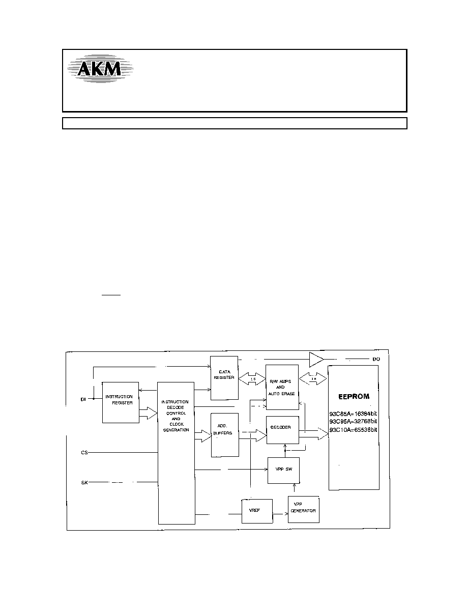
Block Diagram
ASAHI KASEI
[AK93C85A/95A/10A]
DAM02E-01
1999/10
- 2 -
General Description
The AK93C85A/95A/10A is a 16384/32768/65536-bit serial CMOS EEPROM divided into 1024/2048/4096
registers of 16 bits each. The AK93C85A/95A/10A has 4 instructions such as READ, WRITE, EWEN and
EWDS. Those instructions control the AK93C85A/95A/10A.
The AK93C85A/95A/10A can operate full function under wide operating voltage range from 1.8V to 5.5V. The
charge up circuit is integrated for high voltage generation that is used for write operation.
A serial interface of AK93C85A/95A/10A, consisting of chip select (CS), serial clock (SK), data-in (DI) and
data-out (DO), can easily be controlled by popular microcontrollers or standard microprocessors.
AK93C85A/95A/10A takes in the write data from data input pin (DI) to a register synchronously with rising
edge of input pulse of serial clock pin (SK). And at read operation, AK93C85A/95A/10A takes out the read
data from a register to data output pin (DO) synchronously with rising edge of SK.
The DO pin is usually in high impedance state. The DO pin outputs "L" or "H" in case of data output or Busy/Ready
signal output.
Software controlled write protection
When Vcc is applied to the part, the part automatically powers up in the ERASE/WRITE Disable state. In the
ERASE/WRITE disable state, execution of WRITE instruction is disabled. Before WRITE instruction is
executed, EWEN instruction must be executed. The ERASE/WRITE enable state continues until EWDS
instruction is executed or Vcc is removed from the part.
Execution of a read instruction is independent of both EWEN and EWDS instructions.
Busy/Ready status signal
After a write instruction, the DO output serves as a Busy/Ready status indicator. After the falling edge of the
CS initiates the self-timed programming cycle, the DO indicates the Busy/Ready status of the chip if the CS is
brought high after a minimum of 250ns (Tcs). DO=logical "0" indicates that programming is still in progress.
DO=logical "1" indicates that the register at the address specified in the instruction has been written with the
new data pattern contained in the instruction and the part is ready for a next instruction.
The Busy/Ready status indicator is only valid when CS is active (high). When CS is low, the DO output goes
into a high impedance state.
The Busy/Ready signal outputs until a start bit (Logic"1") of the next instruction is given to the part.
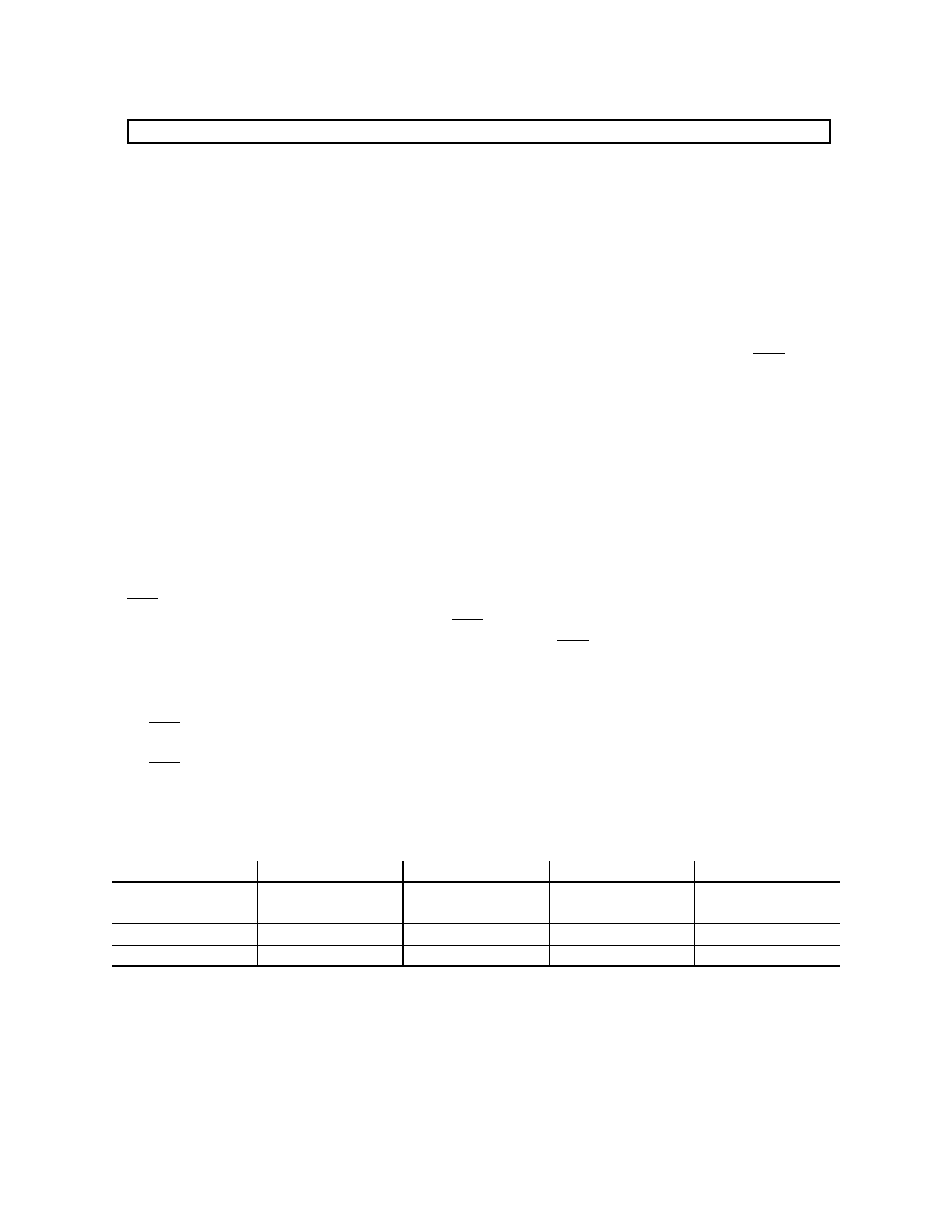
Type of Products
Model
Memory size
Temp.Range
Vcc
Package
AK93C85AF
AK93C85AM
16Kbits
-40
C
85
C
-40
C
85
C
1.8V
5.5V
1.8V
5.5V
8pin Plastic SOP
8pin Plastic SSOP
AK93C95AF
32Kbits
-40
C
85
C
1.8V
5.5V
8pin Plastic SOP
AK93C10AF
64Kbits
-40
C
85
C
1.8V
5.5V
8pin Plastic SOP

ASAHI KASEI
[AK93C85A/95A/10A]
DAM02E-01
1999/10
- 3 -
Pin arrangement
Pin Name
Function
CS
Chip Select
SK
Serial Data Clock
DI
Serial Data Input
DO
Serial Data Output
GND
Ground
Vcc
Power Supply
NC
Not Connected

ASAHI KASEI
[AK93C85A/95A/10A]
DAM02E-01
1999/10
- 4 -
Functional Description
The AK93C85A/95A/10A has 4 instructions such as READ, WRITE, EWEN and EWDS. A valid instruction
consists of a Start Bit (Logic"1"), the appropriate Op Code and the desired memory Address location.
The CS pin must be brought low for a minimum of 250ns (Tcs) between each instruction when the instruction
is continuously executed.
Instruc-
tion
Start
Bit
Op
Code
Address
Data
Comments
READ
1
10
A9-A0
D15-D0
Reads data stored in memory, at specified address.
WRITE
1
01
A9-A0
D15-D0
Writes register.
EWEN
1
00
11XXXXXXXX
Write enable must precede all programming modes.
EWDS
1
00
00XXXXXXXX
Disables all programming instructions.
WRAL
1
00
01XXXXXXXX
D15-D0
Writes all registers.
table1. Instruction Set for the AK93C85A
Instruc-
tion
Start
Bit
Op
Code
Address
Data
Comments
READ
1
10
A10-A0
D15-D0
Reads data stored in memory, at specified address.
WRITE
1
01
A10-A0
D15-D0
Writes register.
EWEN
1
00
11XXXXXXXXX
Write enable must precede all programming modes.
EWDS
1
00
00XXXXXXXXX
Disables all programming instructions.
WRAL
1
00
01XXXXXXXXX
D15-D0
Writes all registers.
table2. Instruction Set for the AK93C95A
Instruc-
tion
Start
Bit
Op
Code
Address
Data
Comments
READ
1
10
A11-A0
D15-D0
Reads data stored in memory, at specified address.
WRITE
1
01
A11-A0
D15-D0
Writes register.
EWEN
1
00
11XXXXXXXXXX
Write enable must precede all programming modes.
EWDS
1
00
00XXXXXXXXXX
Disables all programming instructions.
WRAL
1
00
01XXXXXXXXXX D15-D0
Writes all registers.
table3. Instruction Set for the AK93C10A
(Note)
The WRAL instruction are used for factory function test only.
User can't use the WRAL instruction.
The AK93C85A/95A/10A perceives the start bit in the logic"1" and also "01".
ASAHI KASEI
[AK93C85A/95A/10A]
DAM02E-01
1999/10
- 5 -
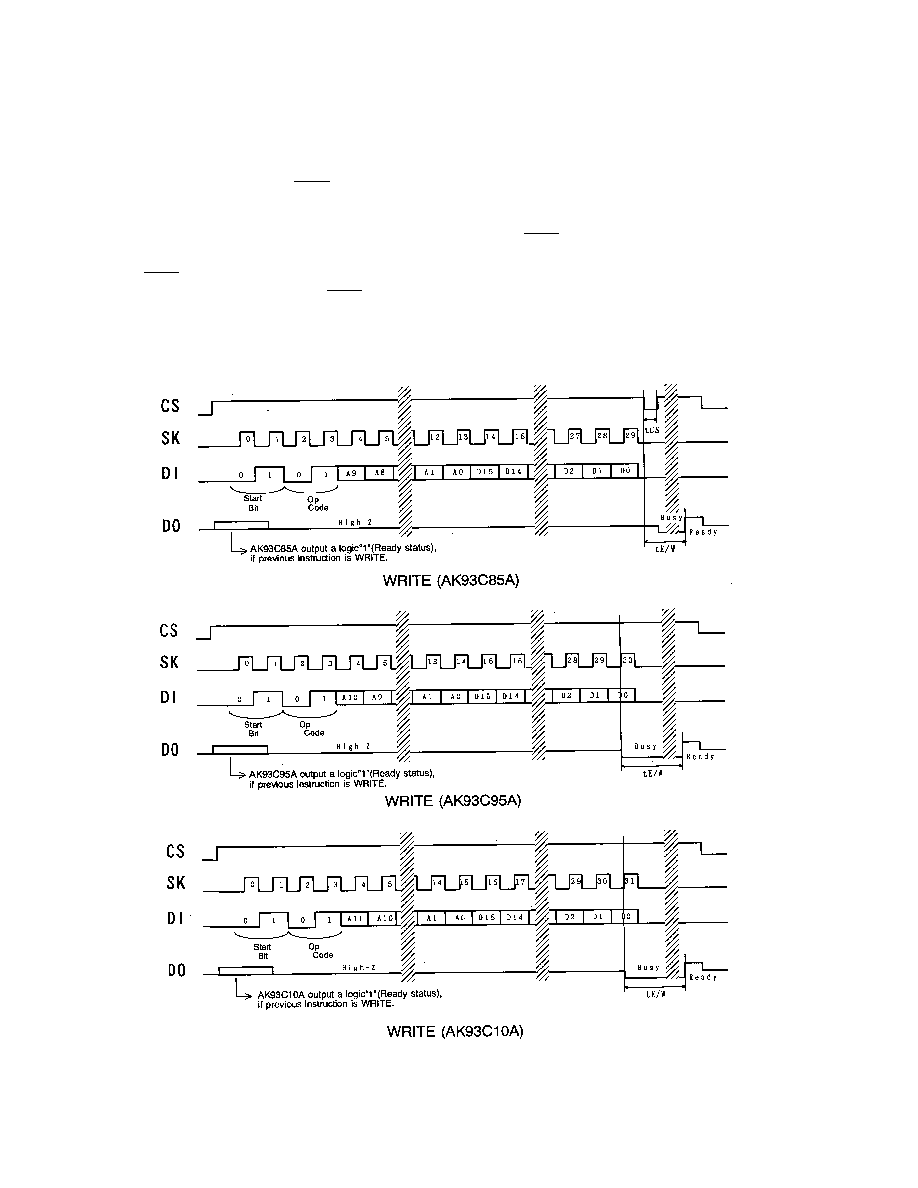
Write
The write instruction is followed by 16 bits of data to be written into the specified address.
AK93C85A : After the last bit of data is put on the DI pin, the CS pin must be brought low
before the next rising edge of the SK clock. This falling edge of the CS initiates the self-timed programming
cycle. The DO indicates the
Busy
/Ready status of the chip if the CS is brought high after a minimum of 250ns
(Tcs).
AK93C95A/10A : The self-timed programming cycle is initiated on the rising edge of the SK
clock as the last data bit (D0) is clocked in. The DO indicates the
Busy
/Ready status of the chip after the self-
timed programming cycle is initiated.
The
Busy
/Ready status indicator is only valid when CS is active (high). When CS is low, the DO output goes
into a high impedance state. The
Busy
/Ready signal outputs until a start bit (Logic"1") of the next instruction
is given to the part.
DO=logical "0" indicates that programming is still in progress. DO=logical "1" indicates that the register at the
address specified in the instruction has been written with the new data pattern contained in the instruction and
the part is ready for a next instruction.