
ASAHI KASEI
[AK9844A]
DAD05E-00
2005/03
- 1 -
AK9844A
4Kbit EEPROM with 4ch 8bit D/A Converter
General Description
The AK9844A includes 4 channel, 8-bit D/A converters with on-chip output buffer amps and it is
capable to store the input digital data of each D/A converter by on-chip non-volatile CMOS
EEPROM. The AK9844A is optimally designed for various circuit adjustments for consumer and
industrial equipments and it is ideally suited for replacing mechanical trimmers.
Features
EEPROM section
4 word x 8-bit organization (Dedicated for DAC data)
256 word x 16-bit organization (General purpose memory)
Serial data interface
Sequential register read
Automatic write cycle
100K write cycles
10 year data retention
D/A section
4 channels
Resolution :
8-bits
Differential Non-Linearity : �1.0 LSB
Linearity Error
: �1.5 LSB
Output Voltage Range
: GND to VCC
AUTO READ Function
Power down mode
Block Diagram
8bit D/A
8bit D/A
8bit D/A
8bit Latch
8bit Latch
8bit Latch
EEPROM
4128bit
256 x 16bit
+ 4 x 8bit
8
8
CS
Control Logic
Instruction
Register
Data
Register
Latch Decoder
SK
PROTECT
PD
8
8bit Latch
+
--
8bit D/A
AO0
8
+
--
AO2
8
+
--
AO3
8
+
--
AO1
VREF1
DI
DO
VCC
GND
VREF2
ASAHI KASEI
[AK9844A]
DAD05E-00
2005/03
- 2 -
Ordering Guide
AK9844AV
-40�C to +85�C
16-pin TSSOP
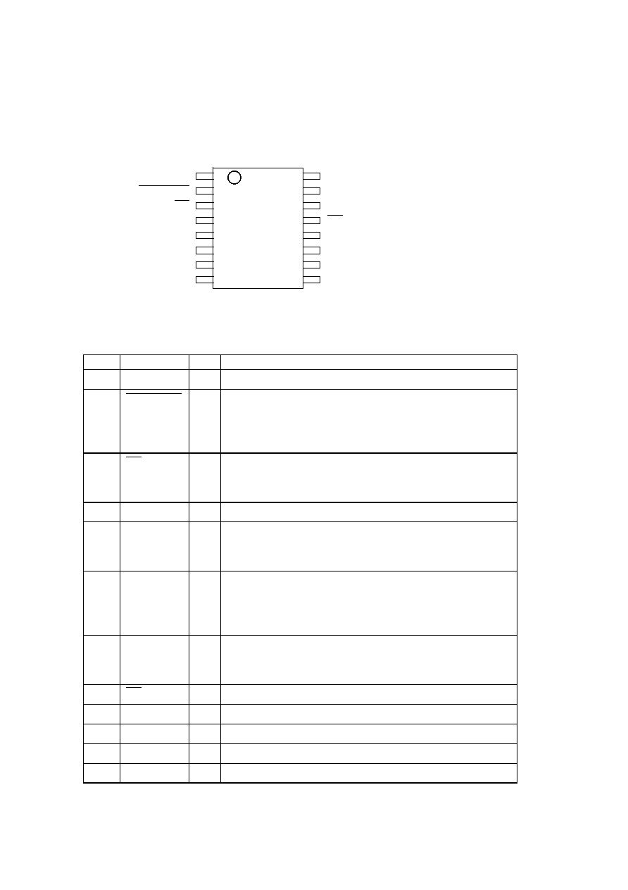
Pin Layout
Pin Description
No. Pin
Name I/O
Function
1
GND
-
Ground Pin, 0V
2
PROTECT
I
Protect Pin
"L" : Programming to the D/A Section of EEPROM is
disabled.
"H" : Normal operation
3
PD
I
Power-down Pin
"L" : Power down mode
"H" : Normal mode
4 VCC
- Power
Supply
6
VREF1
I
Voltage Reference Input1
The analog output ranges of the AO0 and the AO1 are
set by the VREF1 pin.
7
8
9
10
AO0
AO1
AO2
AO3
O
Analog Output Pins (8-bit D/A outputs)
11
VREF2
I
Voltage Reference Input1
The analog output ranges of the AO2 and the AO3 are
set by the VREF2 pin.
13
CS
I
Chip Select Pin
(Schmitt-trigger input)
14
SK
I
Serial Clock Pin
(Schmitt-trigger input)
15
DO
O
Serial Data Output Pin
16
DI
I
Serial Data Input Pin
5, 12 NC
-
Not Connected
DI
DO
CS
SK
NC
VREF2
AO2
AO3
GND
PROTECT
PD
VCC
NC
VREF1
AO0
AO1
16
15
14
13
1
2
3
4
AK9844AV
12
11
10
9
5
6
7
8
16pin TSSOP
ASAHI KASEI
[AK9844A]
DAD05E-00
2005/03
- 3 -
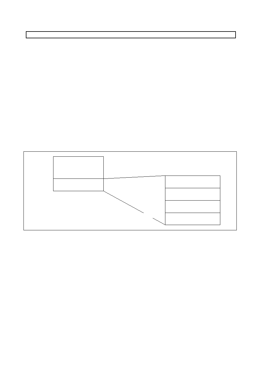
Functional Description
The AK9844A includes the EEPROM section and the D/A converter section which consists of 4
channel, 8bit D/A converters with output buffer amps. The EEPROM section is divided into
memory block and DAC register block. The capacity of the memory block is 4096bits which are
organized into 256 registers of 16bits each. The DAC digital input data for D/A converters are
stored in the DAC register block which is organized into 4 registers of 8bits each. The address for
the memory block is "000000000" to "011111111". The address for the DAC register is
"100000000" to "100000011".
The configuration of the EEPROM section is showed on figure.1.
The AK9844A can connect to the serial communication port of popular one chip microcontrollers
directly (3 line negative clock synchronous interface). At write operation, the AK9844A takes in the
write data from the DI pin to a register synchronously with rising edge of the SK pin. At read
operation, the AK9844A takes out the read data from a register to the DO pin synchronously with
falling edge of the SK pin.
The AK9844A has 6 instructions such as READ, WRITE, WREN, WRDS, PDEN and PDDS. The
each instruction is organized by op-code block(8bits), address block(8bits), and data(8bits x 2).
The output of DAC is set by storing the DAC digital input data in the DAC register block.
The DO pin is high impedance except that the DO pin outputs the read data and the status signal.
Figure 1. Configuration of the EEPROM section
DAC Register Block
Memory Block
Digital input data
for DAC (A00)
000000000
011111111
100000000
100000011
$000
$0FF
$103
100000000
100000001
100000010
$100
$100
$101
$102
$103
100000011
Digital input data
for DAC (A01)
Digital input data
for DAC (A02)
Digital input data
for DAC (A03)
ASAHI KASEI
[AK9844A]
DAD05E-00
2005/03
- 4 -
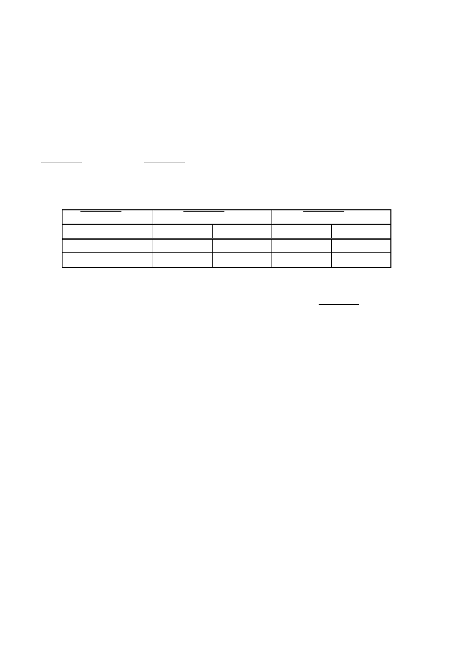
Data Protection
To protect against accidental data disturb, the AK9844A has programming enable state and
programming disable state. In programming disable state, the programming operation is not
executed.
When VCC is applied to the AK9844A, the AK9844A is powered up in the programming disable
mode. The programming instruction should be preceded by the WREN instruction. Once the
WREN instruction is executed, the programming state remains enabled until the WRDS instruction
is executed or VCC is removed from the device. Execution of the READ instruction is independent
of both WREN and WRDS instructions.
The AK9844A also can prohibit to program into the DAC register block by the control of the
PROTECT pin. When the PROTECT pin is "L", the programming into the DAC register block is not
executed.
PROTECT pin
PROTECT="H"
PROTECT="L"
Programming
State
Enable Disable Enable Disable
Memory Block
�
�
DAC Register Block
�
�
�
: Programming into the block is executed.
�
: Programming into the block is not executed.
Table 1. Relation between the programming operation and the PROTECT pin

ASAHI KASEI
[AK9844A]
DAD05E-00
2005/03
- 5 -
Output of D/A converter
The AK9844A includes 4 channel, 8bit D/A converter. The output voltage ranges for AO0 and AO1
are set by the VREF1 pin and the output voltage ranges for AO2 and AO3 are set by the VREF2 pin.
The output voltage can be set by the READ or WRITE instruction.
When the DAC register block is specified in the WRITE instruction, the output voltage for the
specified D/A converter is set. When the WRITE instruction is executed in case that the PROTECT
pin is "H" and the programming state is enabled, the output voltage for the specified D/A converter is
set and the specified address in the DAC register block in EEPROM is written with the data
specified in the instruction.
When the WRITE instruction is executed in case that the PROTECT pin is "H" and the programming
state is disabled, the output voltage for the specified D/A converter is set and the specified address
in the DAC register block in EEPROM is not written with the data specified in the instruction. When
the WRITE instruction is executed in case that the PROTECT pin is "L", the output voltage for the
specified D/A converter is not set and the specified address in the DAC register block in EEPROM is
not written with the data specified in the instruction. The relation between the WRITE instruction
and the DAC register block is showed on the Table 2.
When the DAC register block is specified in the READ instruction, the output voltage for the
specified D/A converter is set by the data which is stored in the DAC register block in EEPROM, and
the DO pin outputs the data in the specified address.
Execution of the READ instruction is independent of the PROTECT pin and the programming state.
PROTECT
pin
Programming
State
DAC register block
(EEPROM section)
Output of DAC
(D/A Converter section)
Enable
The specified address in the
DAC register block is written
with the data specified in the
instruction.
"H"
Disable
The output voltage for the
specified D/A converter is set
by the data specified in the
instruction.
Enable
"L"
Disable
The data in the DAC register
section does not change.
The output of the DAC does
not change.
Table 2. Relation between the WRITE instruction and the DAC register block
AUTO READ Function
When VCC is applied to the AK9844A, the data on EEPROM are read out and loaded at a time to
each corresponding D/A (4 channels total) automatically, starting from AO0 to AO3 in ascending
order. Then each D/A analog output is settled to pre-determined value.
If the CS pin goes to "H" and then goes to "L" after "power-up" with the PROTECT pin and the CS
pin left "L", AUTO READ cycle is initiated. After the CS pin goes to "L", 4 channel D/A outputs are
settled to pre-determined value within 2ms.
In AUTO READ cycle, the SK pin and the DI pin become "don't care" and the serial data do not
output.
If the WREN instruction is executed after AUTO READ cycle is completed, programming into the
memory block on the internal EEPROM is enabled.