 | –≠–ª–µ–∫—Ç—Ä–æ–Ω–Ω—ã–π –∫–æ–º–ø–æ–Ω–µ–Ω—Ç: AKD4363 | –°–∫–∞—á–∞—Ç—å:  PDF PDF  ZIP ZIP |

ASAHI KASEI
[AK4363]
MS0015-E-01
2000/07
- 1 -
GENERAL DESCRIPTION
The AK4363 is a stereo CMOS D/A Converter and Phase Locked Loop for use in digital video broadcast
set-top box applications or DVD. The DAC signal outputs are single-ended and are analog filtered to
remove out of band noise. Therefore no external filters are required. The PLL provides selectable
sampling clock frequencies locked to the 27MHz recovered MPEG clock.
FEATURES
o
Stereo
DAC
o
S/(N+D): 90dB@5V
o
DR:
102dB@5V
o
S/N:
102dB@5V
o
Multiple Sampling Frequencies:
16kHz, 22.05kHz, 24kHz (Half speed)
32kHz, 44.1kHz, 48kHz
(Normal speed)
64kHz, 88.2kHz, 96kHz
(Double speed)
o
On-Chip Low Jitter Analog PLL:
Multiple Master Clock Frequencies generated from 27MHz
256fs/384fs/512fs/768fs/1024fs/1536fs
for Half speed
256fs/384fs/512fs/768fs
for Normal speed
128fs/192fs/256fs/384fs
for Double speed
o
Master Clock: PLL / External
o
Data Input Formats:
LSB justified / MSB justified / I
2
S selectable
o
Selectable Function:
Soft Mute
Digital Attenuator (256 Steps)
Digital De-emphasis (44.1kHz/48kHz/32kHz)
o
Output Mode: Stereo, Mono, Reverse, Mute
o
Input Level:TTL/CMOS Selectable
o
Output Level: 3.0Vpp@5V
o
Control mode: 3-wire Serial / I
2
C Bus
o
Low Power Dissipation: 80mW@5V
o
Small 24pin VSOP Package
o
Power Supply: 2.7
5.5V
o
Ta: -40
85
∞
C
96kHz 24Bit
DAC with PLL
AK4363

ASAHI KASEI
[AK4363]
MS0015-E-01
2000/07
- 2 -
n
Block Diagram
Modulator
MCKO
LRCK
AOUTL
PDN
DVDD
DVSS
8X
Interpolator
PLL &
Clock Generator
LPF
Modulator
AOUTR
8X
Interpolator
LPF
BICK
SDTI
Serial Input
Interface
MCKI
AVDD
AVSS
VCOM
CCLK CDTI
CSN
ATT
ATT
Mixer
DZF
I2C
CAD0
CAD1
TTL
FLT
Figure 1. 3-wire Serial Control Mode (I2C = "L")
Modulator
MCKO
LRCK
AOUTL
PDN
DVDD
DVSS
8X
Interpolator
PLL &
Clock Generator
LPF
Modulator
AOUTR
8X
Interpolator
LPF
BICK
SDTI
Serial Input
Interface
MCKI
AVDD
AVSS
VCOM
SCL
SDA
CSN
ATT
ATT
Mixer
DZF
I2C
CAD0
CAD1
TTL
FLT
Figure 2. I
2
C Bus Control Mode (I2C = "H")

ASAHI KASEI
[AK4363]
MS0015-E-01
2000/07
- 3 -
n
Ordering Guide
AK4363VF
-40
+85
∞
C
24pin VSOP
AKD4363
Evaluation Board
n
Pin Layout
6
5
4
3
2
1
MCKO
NC
DVSS
DVDD
MCKI
BICK
SDTI
7
LRCK
8
DZF
FLT
AVDD
AVSS
VCOM
AOUTL
AOUTR
CAD1
Top
View
10
9
PDN
CSN
SCL/CCLK
11
SDA/CDTI
12
CAD0
I2C
TTL
TST
19
20
21
22
23
24
18
17
15
16
14
13
ASAHI KASEI
[AK4363]
MS0015-E-01
2000/07
- 4 -
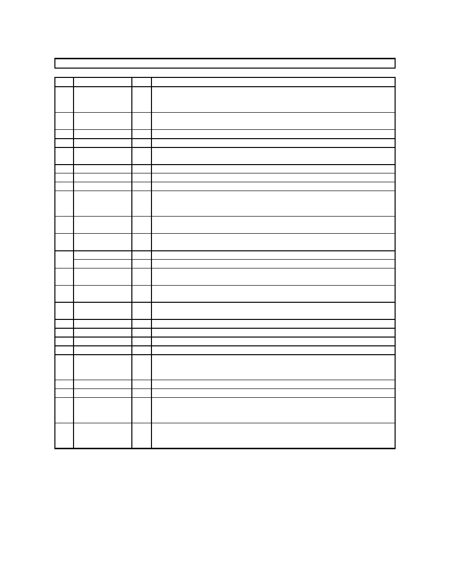
PIN/FUNCTION
No.
Pin Name
I/O
Description
1
MCKO
O
Master Clock Output Pin
EXT = "0": System clock is output from PLL circuit (PLL mode),
EXT = "1": Same frequency as MCKI is output (External mode)
2
NC
-
No Connect
Nothing should be connected externally to this pin.
3
DVDD
-
Digital Power Supply Pin, +2.7
+5.5V
4
DVSS
-
Digital Ground Pin, 0V
5
MCKI
I
System Clock Input Pin
EXT = "0": 27MHz (PLL mode), EXT = "1": Other frequency (External mode)
6
BICK
I
Serial Data Clock Pin
7
SDTI
I
Serial Data Input Pin
8
LRCK
I
Serial Input Channel Clock Pin
9
PDN
I
Power-Down Pin
When "L", the circuit is in power-down mode.
The AK4363 should always be reset upon power-up.
10
CSN
I
Chip Select Pin at 3-wire Serial control mode
This pin should be connected to DVDD at I
2
C Bus control mode.
SCL
I
Control Clock Pin at I
2
C bus control mode
11
CCLK
I
Control Clock Pin at 3-wire serial control mode
SDA
I/O
Control Data Input/Output Pin at I
2
C Bus control mode
12
CDTI
I
Control Data Input Pin at 3-wire serial control mode
13
TST
I
Test pin
This pin should be connected to DVSS.
14
TTL
I
Digital Input Level Select Pin
"L": CMOS, "H": TTL
15
I2C
I
Control Mode Select Pin
"L": 3-wire Serial, "H": I
2
C Bus
16
CAD0
I
Chip Address Select 0 Pin
17
CAD1
I
Chip Address Select 1 Pin
18
AOUTR
O
Rch Analog Output Pin
19
AOUTL
O
Lch Analog Output Pin
20
VCOM
O
Common Voltage Output Pin, AVDD/2
Used for analog common voltage.
Large external capacitor is used to reduce power supply noise.
21
AVSS
-
Analog Ground Pin
22
AVDD
-
Analog Power Supply Pin
23
FLT
O
Output Pin for Loop Filter of PLL Circuit
This pin should be connected to AVSS with one resister and one capacitor in series.
( See "SYSTEM DESIGN".)
24
DZF
O
Zero Input Detect Pin
When SDTI follows a total 8192 LRCK cycles with "0" input data or RSTN = "0",
this pin goes to "H".
Note: No input pins should be left floating.

ASAHI KASEI
[AK4363]
MS0015-E-01
2000/07
- 5 -
ABSOLUTE MAXIMUM RATINGS
(AVSS, DVSS=0V; Note 1)
Parameter
Symbol
min
max
Units
Power Supplies
Analog
Digital
|AVSS-DVSS| (Note 2)
AVDD
DVDD
GND
-0.3
-0.3
-
6.0
6.0
0.3
V
V
V
Input Current (any pins except for supplies)
IIN
-
±
10
mA
Analog Input Voltage
VINA
-0.3
AVDD+0.3
V
Digital Input Voltage
VIND
-0.3
DVDD+0.3
V
Ambient Temperature
Ta
-40
85
∞
C
Storage Temperature
Tstg
-65
150
∞
C
Note:1. All voltages with respect to ground.
2. AVSS and DVSS must be connected to the same analog ground plane.
WARNING: Operation at or beyond these limits may results in permanent damage to the device.
Normal operation is not guaranteed at these extremes.
RECOMMENDED OPERATING CONDITIONS
(AVSS, DVSS=0V; Note 1)
Parameter
Symbol
min
typ
max
Units
3V operation (TTL = "L")
Analog
Digital
AVDD
DVDD
2.7
2.7
3.0
3.0
5.5
3.6 or AVDD
V
V
Power Supplies
(Note 3)
5V operation (TTL = "H")
Analog
Digital
AVDD
DVDD
4.5
4.5
5.0
5.0
5.5
AVDD
V
V
Note:1. All voltages with respect to ground.
3. The power up sequence between AVDD and DVDD is not critical.
*AKM assumes no responsibility for the usage beyond the conditions in this datasheet.