 | –≠–ª–µ–∫—Ç—Ä–æ–Ω–Ω—ã–π –∫–æ–º–ø–æ–Ω–µ–Ω—Ç: AKD4528 | –°–∫–∞—á–∞—Ç—å:  PDF PDF  ZIP ZIP |

ASAHI KASEI
[AK4528]
MS0011-E-00
2000/1
- 1 -
GENERAL DESCRIPTION
The AK4528 is a high performance 24bit CODEC for the 96kHz recording system. The ADC has an
Enhanced Dual Bit architecture with wide dynamic range. The DAC uses the new developed Advanced
Multi Bit architecture and achieves low outband noise and high jitter tolerance by use of SCF (switched
capacitor filter) techniques.
FEATURES
∑
24bit 2ch ADC
- 64x Oversampling
- Full differential Inputs
- S/(N+D): 94dB
- Dynamic Range, S/N: 108dB
- Digital HPF for offset cancellation
- I/F format: MSB justified or I
2
S
∑
24bit 2ch DAC
- 128x Oversampling
- 24bit 8 times Digital Filter
Ripple:
±
0.005dB, Attenuation: 75dB
- SCF
- Differential Outputs
- S/(N+D): 94dB
- Dynamic Range, S/N: 110dB
- De-emphasis for 32kHz, 44.1kHz and 48kHz sampling
- Output DATT with ≠72dB att
- Soft Mute
- I/F format: MSB justified, LSB justified or I
2
S
∑
High Jitter Tolerance
∑
3-wire Serial Interface for Volume Control
∑
Master Clock
- 256fs/384fs/512fs/768fs/1024fs
∑
5V operation
∑
3V Power Supply Pin for 3V I/F
∑
Small 28pin VSOP package
High Performance 24Bit 96kHz Audio CODEC
AK4528
ASAHI KASEI
[AK4528]
MS0011-E-00
2000/1
- 2 -
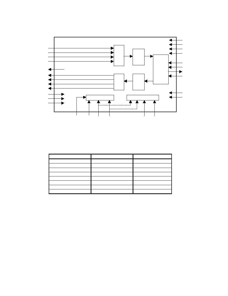
n
Block Diagram
AINL+
AINR+
VCOM
AOUTL+
AOUTL-
AOUTR-
AOUTR+
VREF
VA
AGND
CSN
(DIF)
CCLK
(CKS1)
CDTI
(CKS0)
P/S
MCLK
SDTI
SDTO
BICK
LRCK
DGND
VT
VD
ADC
DAC
HPF
DATT
SMUTE
Audio I/F
Controller
Control Register I/F
Clock Divider
PDN
AINL-
AINR-
DEM1
DEM0
DFS
Block Diagram
∑
Compatibility of AK4528 with AK4524
Function
AK4528
AK4524
ADC S/(N+D)
94dB
90dB
ADC DR, S/N
108dB
100dB
Input PGA & ATT
X
O
ADC Inputs
Differential Inputs
Single-end Inputs
Master Mode
X
O
X'tal Oscillating Circuit
X
O
Quad Speed Mode
X
O
Parallel Mode
O
X
O: Available, X: Not Available

ASAHI KASEI
[AK4528]
MS0011-E-00
2000/1
- 3 -
n
Ordering Guide
AK4528VF
-40
~+85∞C
28pin VSOP (0.65mm pitch)
AKD4528
Evaluation Board
n
Pin Layout
AGND
VCOM
AINR+
AINR-
AINL+
AINL-
VREF
VA
P/S
MCLK
LRCK
BICK
SDTO
SDTI
CDTI(CKS0)
CCLK(CKS1)
CSN(DIF)
DFS
DEM1
VT
VD
DGND
AOUTL-
AOUTL+
AOUTR-
AOUTR+
PDN
DEM0
1
2
3
4
5
6
7
8
9
10
11
12
13
14
15
16
17
18
19
20
21
22
23
24
25
26
27
28
AK4528
Top
View
ASAHI KASEI
[AK4528]
MS0011-E-00
2000/1
- 4 -
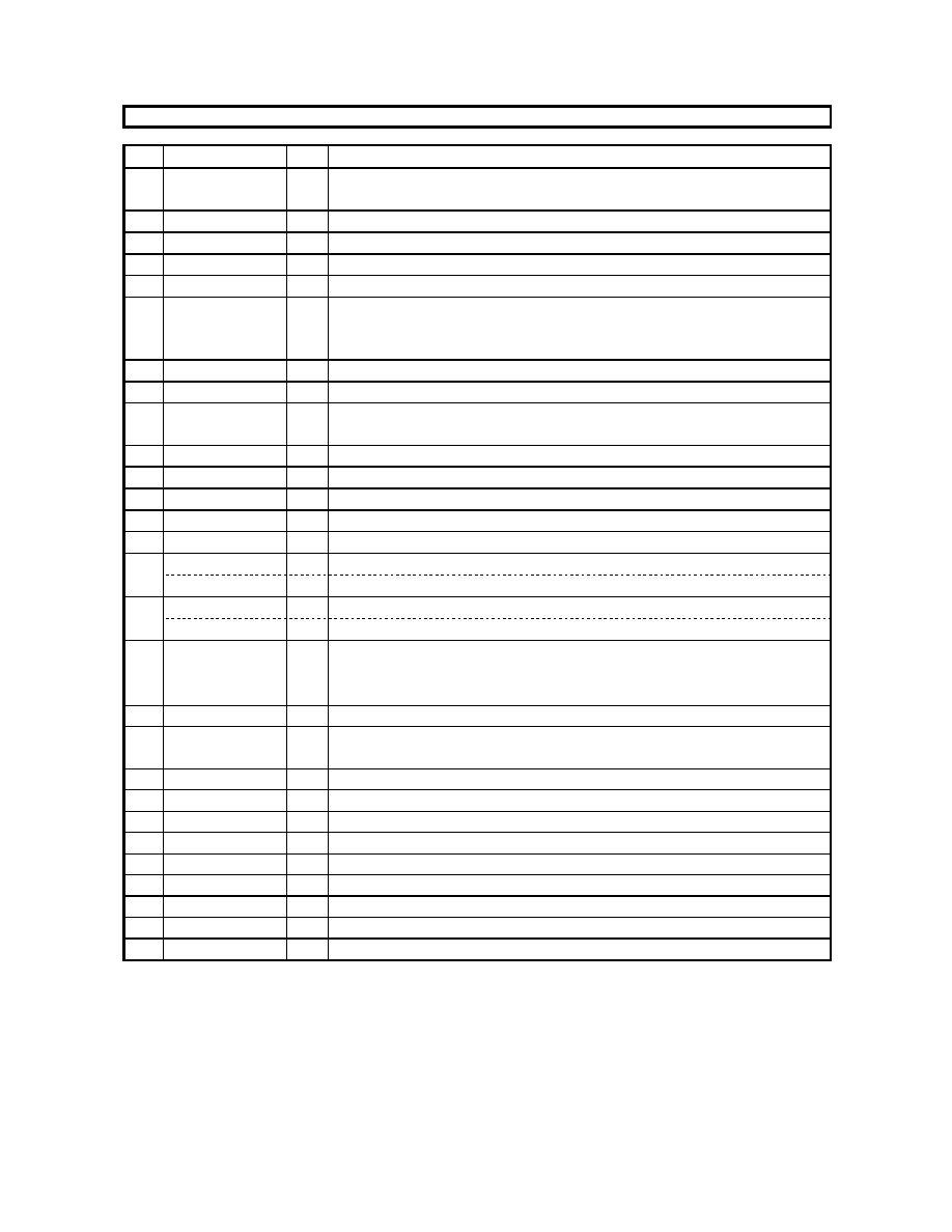
PIN/FUNCTION
No.
Pin Name
I/O
Function
1
VCOM
O
Common Voltage Output Pin, VA/2
Bias voltage of ADC inputs and DAC outputs.
2
AINR+
I
Rch Positive Input Pin
3
AINR-
I
Rch Negative Input Pin
4
AINL+
I
Lch Positive Input Pin
5
AINL-
I
Lch Negative Input Pin
6
VREF
I
Voltage Reference Input Pin, VA
Used as a voltage reference by ADC & DAC. VREF is connected externally to
filtered VA.
7
AGND
-
Analog Ground Pin
8
VA
-
Analog Power Supply Pin, 4.75
~ 5.25V
9
P/S
I
Parallel/Serial Mode Select Pin
"L": Serial Mode, "H": Parallel Mode
10
MCLK
I
Master Clock Input Pin
11
LRCK
I
Input/Output Channel Clock Pin
12
BICK
I
Audio Serial Data Clock Pin
13
SDTO
O
Audio Serial Data Output Pin
14
SDTI
I
Audio Serial Data Input Pin
CDTI
I
Control Data Input Pin in Serial Mode
15
CKS0
I
Master Clock Select Pin
CCLK
I
Control Data Clock Pin in Serial Mode
16
CKS1
I
Master Clock Select Pin
CSN
I
Chip Select Pin in Serial Mode
17
DIF
I
Digital Audio Interface Select Pin
"L": 24bit MSB justified, "H": I
2
S compatible
18
DFS
I
Double Speed Sampling Mode Pin
19
PDN
I
Power-Down Mode Pin
"H": Power up, "L": Power down reset and initialize the control register.
20
DEM0
I
De-emphasis Control Pin
21
DEM1
I
De-emphasis Control Pin
22
VT
-
Output Buffer Power Supply Pin, 2.7
~ 5.25V
23
VD
-
Digital Power Supply Pin, 4.75
~ 5.25V
24
DGND
-
Digital Ground Pin
25
AOUTL-
O
Lch Negative Analog Output Pin
26
AOUTL+
O
Lch Positive Analog Output Pin
27
AOUTR-
O
Rch Negative Analog Output Pin
28
AOUTR+
O
Rch Positive Analog Output Pin
Note: All input pins should not be left floating.

ASAHI KASEI
[AK4528]
MS0011-E-00
2000/1
- 5 -
ABSOLUTE MAXIMUM RATINGS
(AGND, DGND=0V; Note 1)
Parameter
Symbol
min
max
Units
Power Supplies:
Analog
Digital
Output Buffer
VD-VA
VA
VD
VT
VDA
-0.3
-0.3
-0.3
-
6.0
6.0
6.0
0.3
V
V
V
V
Input Current, Any Pin Except Supplies
IIN
-
±10
mA
Analog Input Voltage
VINA
-0.3
VA+0.3
V
Digital Input Voltage
VIND
-0.3
VA+0.3
V
Ambient Temperature (powered applied)
Ta
-40
85
∞C
Storage Temperature
Tstg
-65
150
∞C
Note: 1. All voltages with respect to ground.
WARNING: Operation at or beyond these limits may result in permanent damage to the device.
Normal operation is not guaranteed at these extremes.
RECOMMENDED OPERATING CONDITIONS
(AGND, DGND=0V; Note 1)
Parameter
Symbol
min
typ
max
Units
Power Supplies
Analog
Digital
Output Buffer
VA
VD
VT
4.75
4.75
2.7
5.0
5.0
3.0
5.25
VA
VD
V
V
V
Voltage Reference
VREF
3.0
-
VA
V
Note:1. All voltages with respect to ground.
2. VA and VD should be powered at the same time or VA should be powered earlier than VD.
The power up sequence between VA and VT, or VD and VT is not critical.
*AKM assumes no responsibility for the usage beyond the conditions in this datasheet.

ASAHI KASEI
[AK4528]
MS0011-E-00
2000/1
- 6 -
ANALOG CHARACTERISTICS
(Ta=25
∞C; VA, VD, VT=5.0V; AGND=DGND=0V; VREF=VA; fs=44.1kHz; Signal Frequency =1kHz; 24bit Data;
Measurement frequency = 20Hz
~ 20kHz at fs=44.1kHz, 40Hz ~ 40kHz at fs=96kHz; unless otherwise specified)
Parameter
min
typ
max
Units
Input PGA Characteristics:
ADC Analog Input Characteristics: Analog Source impedance = 330
W
W
W
W
Resolution
24
Bits
Input Voltage (Note 3)
±2.6
±2.8
±3.0
Vpp
Input Resistance
fs=44.1kHz
fs=96kHz
16
7
27
12
k
W
k
W
S/(N+D) (-0.5dBFS)
fs=44.1kHz
fs=96kHz
88
84
94
92
dB
dB
DR (-60dBFS)
fs=44.1kHz, A-weighted
fs=96kHz
100
95
108
103
dB
dB
S/N
fs=44.1kHz, A-weighted
fs=96kHz
100
95
108
103
dB
dB
Interchannel Isolation
90
110
dB
Interchannel Gain Mismatch
0.2
0.5
dB
Gain Drift
20
-
ppm/
∞C
Input Voltage (Note 3)
±2.6
±2.8
±3.0
Vpp
Input Resistance
fs=44.1kHz
fs=96kHz
16
7
27
12
k
W
k
W
Input DC Bias Voltage (Note 4)
0.56VA
-
0.60VA
V
Power Supply Rejection (Note 5)
-
50
-
dB
DAC Analog Output Characteristics:
Resolution
24
Bits
S/(N+D) (0dBFS)
fs=44.1kHz
fs=96kHz
88
85
94
93
dB
dB
DR (-60dBFS)
fs=44.1kHz, A-weighted
fs=96kHz
104
96
110
104
dB
dB
S/N
fs=44.1kHz, A-weighted
fs=96kHz
104
96
110
104
dB
dB
Interchannel Isolation
90
110
dB
Interchannel Gain Mismatch
0.2
0.5
dB
Gain Drift
20
-
ppm/
∞C
Output Voltage (Note 6)
5.0
5.4
5.8
Vpp
Load Resistance (In case of AC load)
1
k
W
Output Current
1.5
mA
Load Capacitance
25
pF
Power Supply Rejection (Note 5)
50
-
dB
Note: 3. This voltage is input to AIN+ and AIN- pin, and is proportional to VREF. Vin = 0.56 x VREF.
4. Measured by Figure 12. DC Bias Voltage, Vb = 4.7k / (3.3k + 4.7k) x VA = 0.5875VA.
5. PSR is applied to VA, VD, VT with 1kHz, 50mVpp. VREF pin is held a constant voltage.
6. Full scale (0dB) of the output voltage when summing the differential outputs, AOUT+/- by unity gain.
This voltage is proportional to VREF. Vout=1.08 x VREF x Gain.

ASAHI KASEI
[AK4528]
MS0011-E-00
2000/1
- 7 -
Parameter
min
typ
max
Units
Power Supplies
Power Supply Current
Normal Operation (PDN="H")
VA
VD+VT (fs=44.1kHz)
(fs=96kHz)
Power-down mode (PDN="L") (Note 7)
VA
VD+VT
38
10
18
10
10
57
20
36
100
100
mA
mA
mA
mA
mA
Note: 7. All digital input pins are held VD or DGND.
FILTER CHARACTERISTICS
(Ta=25
∞C; VA, VD=4.75 ~ 5.25V; VT=2.7 ~ 5.25V; fs=44.1kHz; DEM=OFF)
Parameter
Symbol
min
typ
max
Units
ADC Digital Filter (Decimation LPF):
Passband (Note 8)
-0.005dB
-0.02dB
-0.06dB
-6.0dB
PB
0
-
-
-
20.02
22.20
22.05
19.76
-
-
-
kHz
kHz
kHz
kHz
Stopband
SB
24.34
kHz
Passband Ripple
PR
±0.005
dB
Stopband Attenuation
SA
80
dB
Group Delay (Note 9)
GD
31
1/fs
Group Delay Distortion
DGD
0
us
ADC Digital Filter (HPF):
Frequency Response (Note 8)
-3dB
-0.5dB
-0.1dB
FR
0.9
2.7
6.0
Hz
Hz
Hz
DAC Digital Filter:
Passband (Note 8)
-0.01dB
-6.0dB
PB
0
-
22.05
20.0
-
kHz
kHz
Stopband
SB
24.1
kHz
Passband Ripple
PR
±0.005
dB
Stopband Attenuation
SA
75
dB
Group Delay (Note 9)
GD
30
1/fs
DAC Digital Filter + SCF:
Frequency Response:
0
~ 20.0kHz
~ 40kHz (Note 10)
FR
±0.2
±0.3
dB
dB
Note: 8. The passband and stopband frequencies scale with fs.
For example, 20.02kHz at -0.02dB is 0.454 x fs. The reference frequency of these responses is 1kHz.
9. The calculating delay time which occurred by digital filtering. This time is from the input of analog signal to
setting the 24bit data of both channels to the output register for ADC.
For DAC, this time is from setting the 24bit data of both channels on input register to the output of analog signal.
10. fs=96kHz.

ASAHI KASEI
[AK4528]
MS0011-E-00
2000/1
- 8 -
DC CHARACTERISTICS
(Ta=25
∞C; VA,VD=4.75 ~ 5.25V; VT=2.7 ~ 5.25V)
Parameter
Symbol
min
typ
max
Units
High-Level Input Voltage
Low-Level Input Voltage
VIH
VIL
2.2
-
-
-
-
0.8
V
V
High-Level Output Voltage (Iout=-100
mA) (Note 11)
Low-Level Output Voltage (Iout=100
mA)
VOH
VOL
2.7 / VT-0.5
-
-
-
-
0.5
V
V
Input Leakage Current
Iin
-
-
±10
µA
Note: 11. The min value is lower voltage of 2.7V or VT-0.5V.
SWITCHING CHARACTERISTICS
(Ta=25
∞C; VA,VD=4.75 ~ 5.25V, VT=2.7 ~ 5.25V; C
L
=20pF)
Parameter
Symbol
min
typ
max
Units
Master Clock Timing
Frequency
Pulse Width Low
Pulse Width High
fCLK
tCLKL
tCLKH
7.68
0.4/fCLK
0.4/fCLK
55.296
MHz
ns
ns
LRCK Frequency
Normal Speed Mode (DFS = "0")
Double Speed Mode (DFS = "1")
Duty Cycle
fsn
fsd
Duty
30
60
45
44.1
88.2
54
108
55
kHz
kHz
%
Audio Interface Timing
BICK Period
BICK Pulse Width Low
Pulse Width High
LRCK Edge to BICK "
" (Note 12)
BICK "
" to LRCK Edge (Note 12)
LRCK to SDTO (MSB) (Except I
2
S mode)
BICK "
Ø" to SDTO
SDTI Hold Time
SDTI Setup Time
tBCK
tBCKL
tBCKH
tLRB
tBLR
tLRS
tBSD
tSDH
tSDS
81
33
33
20
20
20
20
40
40
ns
ns
ns
ns
ns
ns
ns
ns
ns
Note 12. BICK rising edge must not occur at the same time as LRCK edge.

ASAHI KASEI
[AK4528]
MS0011-E-00
2000/1
- 9 -
Parameter
Symbol
min
typ
max
Units
Control Interface Timing (P/S="L")
CCLK Period
CCLK Pulse Width Low
Pulse Width High
CDTI Setup Time
CDTI Hold Time
CSN "H" Time
CSN "L" Time
CSN "
" to CCLK ""
CCLK "
" to CSN ""
tCCK
tCCKL
tCCKH
tCDS
tCDH
tCSW
tCSW
tCSS
tCSH
200
80
80
40
40
150
150
150
50
ns
ns
ns
ns
ns
ns
ns
ns
ns
Reset Timing
PDN Pulse Width (Note 13)
RSTADN "
" to SDTO valid (Note 14)
PDN "
" to SDTO valid (Note 15)
tPD
tPDV
tPDV
150
516
516
ns
1/fs
1/fs
Note:13. The AK4528 can be reset by bringing PDN "L".
14. In serial mode, these cycles are the number of LRCK rising from RSTADN bit.
15. In parallel mode, these cycles are the number of LRCK rising from PDN pin.
n
Timing Diagram
1/fCLK
tCLKL
VIL
tCLKH
MCLK
VIH
1/fs
LRCK
VIH
VIL
tBCK
tBCKL
VIH
tBCKH
BICK
VIL
Clock Timing

ASAHI KASEI
[AK4528]
MS0011-E-00
2000/1
- 10 -
LRCK
BICK
SDTO
SDTI
tBLR
tLRB
tLRS
tBSD
tSDS
tSDH
VIH
VIL
VIH
VIL
50%VT
VIH
VIL
Audio Interface Timing
CSN
CCLK
CDTI
tCSS
tCCKL tCCKH
tCDS
tCDH
C1
C0
R/W
A4
VIH
VIL
VIH
VIL
VIH
VIL
WRITE Command Input Timing
CSN
CCLK
CDTI
tCSW
tCSH
D3
D2
D1
D0
VIH
VIL
VIH
VIL
VIH
VIL
WRITE Data Input Timing
tPD
VIL
PDN
Power Down & Reset Timing

ASAHI KASEI
[AK4528]
MS0011-E-00
2000/1
- 11 -
OPERATION OVERVIEW
n
System Clock Input
The external clocks, which are required to AK4528, are MCLK, BICK and LRCK. MCLK should be synchronized with
LRCK but the phase is not critical. The frequency of MCLK is set by CMODE, CKS0-1 and DFS bits in serial mode, or by
CKS0-1, DFS pins in parallel mode (see Table 2 and 3). The CKS0-1 and DFS pin should be changed during the PDN pin
= "L". The CMODE, CKS0-1 and DFS bits are changed during RSTADN=RSTDAN= "0".
External clocks (MCLK, BICK and LRCK) should always be present whenever the AK4528 is in normal operation mode
(PDN="H" and at least one of ADC and DAC is in normal operation mode). If these clocks are not provided, the AK4528
may draw excess current because the device utilizes dynamic refreshed logic internally. If the external clocks are not
present, the AK4528 should be in the power-down mode (PDN="L" or set both ADC and DAC power down mode by the
register).
CMODE bit
CKS1 bit
CKS0 bit
MCLK
Normal Speed
(DFS bit="0")
MCLK
Double Speed
(DFS bit="1")
0
0
0
256fs
N/A
0
0
1
512fs
256fs
0
1
0
1024fs
512fs
1
0
0
384fs
N/A
1
0
1
768fs
384fs
Default
Table 1. Master Clock Frequency Select in Serial Mode
CKS1 pin
CKS0 pin
MCLK
Normal Speed
(DFS pin = "L")
MCLK
Double Speed
(DFS pin = "H")
L
L
256fs
N/A
L
H
512fs
256fs
H
L
384fs
N/A
H
H
1024fs
512fs
Table 2. Master Clock Frequency Select in Parallel Mode
MCLK
Normal Speed
(DFS = "0")
fs=44.1kHz
fs=48kHz
MCLK
Double Speed
(DFS = "1")
fs=88.2kHz
fs=96kHz
256fs
11.2896MHz
12.288MHz
N/A
N/A
N/A
512fs
22.5792MHz
24.576MHz
256fs
22.5792MHz
24.576MHz
1024fs
45.1584MHz
49.152MHz
512fs
45.1584MHz
49.152MHz
384fs
16.9344MHz
18.432MHz
N/A
N/A
N/A
768fs
33.8688MHz
36.864MHz
384fs
33.8688MHz
36.864MHz
Table 3. Master Clock Frequencies example
Note. Do not set any mode which is not described in Table1-3.

ASAHI KASEI
[AK4528]
MS0011-E-00
2000/1
- 12 -
n
Audio Serial Interface Format
In case of serial mode, the DIF0-2 bits as shown in Table 4 support five serial formats. In case of parallel mode, two
formats (Mode 2 and 3) are supported by DIF pin (Table 5). In all modes the serial data is MSB-first, 2's compliment
format. The SDTO is clocked out on the falling edge of BICK and the SDTI is latched on the rising edge.
Mode
DIF2 bit
DIF1 bit
DIF0 bit
SDTO
SDTI
LRCK
BICK
0
0
0
0
24bit, MSB justified
16bit, LSB justified
H/L
≥ 32fs
1
0
0
1
24bit, MSB justified
20bit, LSB justified
H/L
≥ 40fs
2
0
1
0
24bit, MSB justified
24bit, MSB justified
H/L
≥ 48fs
3
0
1
1
24bit, I
2
S
24bit, I
2
S
L/H
≥ 48fs
4
1
0
0
24bit, MSB justified
24bit, LSB justified
H/L
≥ 48fs
Default
Table 4. Audio data format in Serial Mode
Mode
DIF pin
SDTO
SDTI
LRCK
BICK
2
0
24bit, MSB justified
24bit, MSB justified
H/L
≥ 48fs
3
1
24bit, I
2
S
24bit, I
2
S
L/H
≥ 48fs
Table 5. Audio data format in Parallel Mode
LRCK
BICK(64fs)
SDTO(o)
0
1
2
19
17
18
20
31
0
1
2
19
17
18
20
31
0
23
1
22
4
23 22
7
6
4
23
SDTI(i)
1
14
0
12
11
1
14
0
12
11
SDTO-19:MSB, 0:LSB; SDTI-15:MSB, 0:LSB
Lch Data
Rch Data
Don't Care
Don't Care
7
6
BICK(32fs)
SDTO(o)
0
1
2
9
10
12
13
15
0
1
2
9
10
12
13
15
0
23
1
22
12
23 22
12
15 14
23
SDTI(i)
1
6
0
4
3
1
15
0
5
4
15 14
2
9
8
11
10
21
15 14 13
3
11
14
13
5
7
21
5
3
13
15
30
21
3
3
21
14
13
7
6
3
2
15
14
11
8
9
10
11
13
5
3
15
13
2
2
Figure 1. Mode 0 Timing
LRCK
BICK(64fs)
SDTO(o)
0
1
2
12
13
14
24
25
31
0
1
2
12
13
14
24
25
31
0
23
1
22
0
23 22
12
11 10
0
23
SDTI(i)
1
18
0
19
8
7
1
18
0
19
8
7
SDTO-23:MSB, 0:LSB; SDTI-19:MSB, 0:LSB
Lch Data
Rch Data
Don't Care
Don't Care
12
11 10
Figure 2. Mode 1 Timing

ASAHI KASEI
[AK4528]
MS0011-E-00
2000/1
- 13 -
LRCK
BICK(64fs)
SDTO(o)
0
1
2
18
19
20
21
22
0
1
2
18
19
20
22
21
0
1
SDTI(i)
23
24
25
23
24
25
23 22
4
23 22
5
4
5
4
1
22
0
23
3
2
1
22
0
23
3
2
23:MSB, 0:LSB
Lch Data
Rch Data
Don't Care
Don't Care
5
5
4
1
0
3
2
1
0
3
2
23
Figure 3. Mode 2 Timing
LRCK
BICK(64fs)
SDTO(o)
0
1
2
3
19
20
21
22
0
1
2
3
19
20
22
21
0
1
SDTI(i)
23
24
25
23
24
25
23 22
4
23 22
5
4
5
4
1
22
0
23
3
2
1
22
0
23
3
2
23:MSB, 0:LSB
Lch Data
Rch Data
Don't Care
Don't Care
5
5
4
1
0
3
2
1
0
3
2
Figure 4. Mode 3 Timing
LRCK
BICK(64fs)
SDTO(o)
0
1
2
8
9
10
20
21
31
0
1
2
8
9
10
20
21
31
0
23
1
22
0
23 22
16
15 14
0
23
SDTI(i)
1
22
0
23
12
11
1
22
0
23
12
11
23:MSB, 0:LSB
Lch Data
Rch Data
Don't Care
Don't Care
16
15 14
Figure 5. Mode 4 Timing

ASAHI KASEI
[AK4528]
MS0011-E-00
2000/1
- 14 -
n
n
n
n
Parallel/Serial Mode Control
When P/S= "H", AK4528 is in parallel mode. The audio interface format is selected by DIF pin, and DFS and CK0-1 pins
select the frequency of MCLK.
When P/S= "L", AK4528 is in serial mode. The CKS1, CKS0 and DIF pins are changed to CDTI, CCLK and CSN pins
respectively. The DEM0-1 and DFS are ORed between pin and register respectively, so those are able to control by pins
even in serial mode. To control all the functions by register, set DEM0-1 and DFS pins "L".
n
n
n
n
Digital High Pass Filter
The ADC has a digital high pass filter(HPF) for DC offset cancel. The cut-off frequency of the HPF is 0.9Hz at fs=44.1kHz
and also scales with sampling rate (fs). This HPF can be off for each channels by register.
n
n
n
n
Output Volume
The AK4528 includes digital volumes (OATT) with 128 levels (including MUTE) in front of DAC. The OATT is a
pseudo-log volume linear-interpolated internally. When the level is changed, the transition to new value takes 8031
levels(max) and is done by soft transition. Therefore, there is not any switching noise.
n
n
n
n
De-emphasis Filter
The DAC includes the digital de-emphasis filter (tc=50/15µs) by IIR filter. This filter supports to three frequencies
(32kHz, 44.1kHz and 48kHz). This setting is done by contorl register and always OFF at double speed mode.
No
DEM1
DEM0
Mode
0
0
0
44.1kHz
1
0
1
OFF
2
1
0
48kHz
3
1
1
32kHz
Default in serial mode
Table 6. De-emphasis control (DFS="0")

ASAHI KASEI
[AK4528]
MS0011-E-00
2000/1
- 15 -
n
Soft Mute Operation
Soft mute operation is performed at digital domain. When SMUTE goes "1", the output signal is attenuated by -
• during
1024 LRCK cycles. When SMUTE is returned to "0", the mute is cancelled and the output attenuation gradually changes
to 0dB during 1024 LRCK cycles. If the soft mute is cancelled within 1024 LRCK cycles after starting of the operation, the
attenuation is discontinued and returned to 0dB.
Soft mute function is independent to output volume, and those two functions are cascade connected.
S M U T E
A tte nuation
102 4/fs
0dB
-
•
102 4/fs
G D
G D
(1)
(2)
(3)
Notes:
(1)
The output signal is attenuated by -
• during 1024 LRCK cycles (1024/fs).
(2)
Analog output corresponding to digital input has the group delay (GD).
(3)
If the soft mute is cancelled within 1024 LRCK cycles, the attenuation is discontinued and returned to 0dB.
Figure 6. Soft Mute

ASAHI KASEI
[AK4528]
MS0011-E-00
2000/1
- 16 -
n
Power Down & Reset
The ADC and DAC of AK4528 are placed in the power-down mode by bringing a power down pin(PDN)="L" and each
digital filter is also reset at the same time. The internal register values are initialized by PDN="L". This reset should always
be done after power-up.
In case of serial mode, the default value of both control registers for ADC and DAC are in reset state (RSTADN=
RSTDAN = "0" ), each register sholud be cancelled after doing the needed setting. In case of the ADC, an analog
initialization cycle starts after exiting the power-down or reset state. Therefore, the output data, SDTO becomes available
after 516 cycles of LRCK. In case of DAC, the initialization cycle starts after PDN= "H" or PWVR bit = "1". The power
down mode can be also controlled by the registers (PWAD, PWDA).
Power Supply
RSTADN(registe
RSTDAN(registe
PWAD(register)
PWDA(register)
PWVR(register)
ADC Internal State
SDTO
OATT
AOUT
DAC Internal State
External Mute
Example
External clocks
The clocks can be stopped.
PD
Reset INITA
Normal
PD
INITA
Normal
"0"
"0"
Output
Output
PD
Reset
PD
Normal
Normal
00H
00H
Æ
XXH
XXH
00H
00H
Æ
XXH
XXH
"0"
FI
Output
FI
MCLK, LRCK, BICK
PDN pin
*
*
*
INITD
*
Hi-Z
Hi-Z
Output
PD
Normal
00H
00H
Æ
XXH
XXH
FI
*
*
Hi-Z
Output
PD
"0"
512/fs
512/fs
INITD
∑ INITA:
Initializing period of ADC analog section (516/fs).
∑ INITD:
Initializing period of DAC analog section (512/fs).
∑ PD:
Power down state. In case of PDN= "L", the contents of all registers are initialized, otherwise hold.
∑ XXH:
The current value in ATT register.
∑ FI:
Fade in. After exiting power down and reset state, ATT value fades in by 8032/fs cycles(max).
∑ AOUT:
Some pop noise may occur at "*".
Figure 7. Reset & Power down sequence in Serial Mode

ASAHI KASEI
[AK4528]
MS0011-E-00
2000/1
- 17 -
In case of parallel mode, both ADC and DAC are powered up with releasing internal reset state when PDN is set to "H".
Therefore each outputs start to output at once. However the initialization of ADC/DAC, and the fade-in cycle of OATT
(8031/fs) are exist.
Power Supply
ADC Internal State
SDTO
OATT
AOUT
DAC Internal State
External Mute
Example
External clocks
The clocks can be stopped.
PD
INITA
Normal
PD
INITA
Normal
"0"
"0"
Output
Output
PD
PD
Normal
Normal
00H
Æ
7FH
7FH
00H
00H
Æ
7FH
7FH
Hi-Z
Hi-Z
FI
Output
FI
MCLK, LRCK, BICK
PDN pin
*
*
00H
MCLK, LRCK, BICK
Output
*
512/fs
512/fs
INITD
INITD
∑ INITA:
Initializing period of ADC analog section (516/fs).
∑ INITD:
Initializing period of DAC analog section (512/fs).
∑ PD:
Power down state.
∑ FI:
Fade in. After exiting power down state, ATT value fades in by 8032/fs cycles.
∑ AOUT:
Some pop noise may occur at "*".
Figure 8. Reset & Power Down Sequence in Parallel Mode

ASAHI KASEI
[AK4528]
MS0011-E-00
2000/1
- 18 -
n
Serial Control Interface
The serial control interface is enabled by the P/S pin = "L". The internal registers are written by the 3 wire uP interface
pins: CSN, CCLK, CDTI. The data on this interface consists of Chip address (2bits, fixed to C0/1 ="01") Read/Write (1bit,
fixed to "1". ), Register address (MSB first, 5bits) and Control data (MSB first, 8bits). Address and data is clocked in on
the rising edge of CCLK. Data is latched after a low-to-high transition of CSN. The maximum clock speed of the CCLK is
5MHz. The CSN should be "H" if no access. The chip address is fixed to "10". Writing is invalid for the access to the chip
address except for "10". PDN = "L" resets the registers to their default values.
Function
Parallel mode
Serial mode
Double speed
O
O
De-emphasis
O
O
SMUTE
X
O
Output Digital ATT
X
O
HPF off
X
O
MCLK;
768fs@Normal
Speed
384fs@Double
Speed
X
O
16/20/24bit LSB justified format
X
O
Table 7. function list (O: available, X: not available)
When PDN = "L", internal registers are initialized. In case of changing P/S pin, please set PDN = "L" to reset the device.
In case of serial mode, the internal timings are initialized by RSTN ="0", but the contents of registers are hold.
CSN
CCLK
0
1
2
3
4
5
6
7
8
9
10
11 12
13 14 15
CDTI
C1 C0
A2
A3
A1 A0
A4
D7 D6 D5 D4 D3 D2 D1 D0
R/W
C1-C0:
Chip Address (Fixed to "10")
R/W:
READ/WRITE (Fixed to "1":WRITE only)
A4-A0:
Register Address
D7-D0:
Control data
Figure 9. Control I/F Timing
*AK4528 does not support the READ. C1,C0 and R/W are fixed ("101").

ASAHI KASEI
[AK4528]
MS0011-E-00
2000/1
- 19 -
n
Register Map
Addr
Register Name
D7
D6
D5
D4
D3
D2
D1
D0
00H
Power Down Control
0
0
0
0
0
PWVR
PWAD
PWDA
01H
Reset Control
TE7
TE6
TE5
TE4
0
0
RSTADN
RSTDAN
02H
Clock and Format Control
DIF2
DIF1
DIF0
CMODE
CKS1
CKS0
0
DFS
03H
Deem and Volume Control
SMUTE
0
0
0
HPFR
HPFL
DEM1
DEM0
04H
Lch ATT Control
0
ATTL6
ATTL5
ATTL4
ATTL3
ATTL2
ATTL1
ATTL0
05H
Rch ATT Control
0
ATTR6
ATTR5
ATTR4
ATTR3
ATTR2
ATTR1
ATTR0
Note: For address from 06H to 1FH, data should not be written.
In case of writing to 01H, write"0000" to D7-4.
PDN = "L" resets the registers to their default values.
n
n
n
n
Control Register Setup Sequence
The setting of clock mode or data format by control register should be done during RSTADN=RSTDAN= "0", and outputs
of ADC/DAC should be muted.
1. In case of using PDN pin
(1)
Set PDN= "H".
(2)
Set registers for clock mode, data format, etc.
(3)
Cancel the reset state by setting RSTADN or RSTDAN to "1". Refer to Reset Contorl Register (01H).
2. In case of not using PDN pin
(1)
Set RSTADN=RSTDAN= "0".
(2)
Set registers for clock mode, data format, etc.
(3)
Cancel the reset state by setting RSTADN or RSTDAN to "1". Refer to Reset Contorl Register (01H).
Note: Those settings may generate pop noise. Please mute the output of ADC and DAC externally.

ASAHI KASEI
[AK4528]
MS0011-E-00
2000/1
- 20 -
n
n
n
n
Register Definitions
Addr
Register Name
D7
D6
D5
D4
D3
D2
D1
D0
00H
Power Down Control
0
0
0
0
0
PWVR
PWAD
PWDA
default
0
0
0
0
0
1
1
1
PWDA: DAC power down
0: Power down
1: Power up
Only DAC section is powered down by "0" and then the AOUTs go Hi-Z immediately. The OATTs also go
"00H". But the contents of all register are not initialized and enabled to write to the registers.
After exiting the power down mode, the OATTs fade in the setting value of the control register (04H &
05H). The analog outputs should be muted externally as some pop noise may occur when entering to and
exiting from this mode.
PWAD: ADC power down
0: Power down
1: Power up
Only ADC section is powered down by "0" and then the SDTO goes "L" immediately. The contents of all
register are not initialized and enabled to write to the registers.
After exiting the power down mode, ADC outputs "0" during first 516 LRCK cycles.
PWVR: Vref power down
0: Power down
1: Power up
All sections are powered down by "0" and then both ADC and DAC do not operate. The contents of all
register are not initialized and enabled to write to the registers. When PWAD and PWDA go "0" and PWVR
goes "1", only VREF section can be powered up.
Addr
Register Name
D7
D6
D5
D4
D3
D2
D1
D0
01H
Reset Control
TE7
TE6
TE5
TE4
0
0
RSTADN
RSTDAN
default
0
0
0
0
0
0
0
0
TE7-4:
Test Control Register Enable
Must be fixed to "0000".
RSTDAN: DAC reset
0: Reset
1: Normal Operation
The internal timing is reset by "0" and then the AOUTs go VCOM voltage immediately. The OATTs also go
"00H". But the contents of all register are not initialized and enabled to write to the registers. After exiting
the power down mode, the OATTs fade in the setting value of the control register (06H & 07H). The analog
outputs should be muted externally as some pop noise may occur when entering to and exiting from this
mode.
RSTDAN: ADC reset
0: Reset
1: Normal Operation
The internal timing is reset by "0" and then SDTO goes "L" immediately. But the contents of all register are
not initialized and enabled to write to the register.
After exiting the power down mode, ADCs output "0" during first 516 LRCK cycles.

ASAHI KASEI
[AK4528]
MS0011-E-00
2000/1
- 21 -
Addr
Register Name
D7
D6
D5
D4
D3
D2
D1
D0
02H
Clock and Format Control
DIF2
DIF1
DIF0
CMODE
CKS1
CKS0
0
DFS
default
0
1
0
0
0
0
0
0
DFS: Sampling Speed Control (see Table 1 and Table 3)
Default : normal speed mode.
Ored with DFS pin internally.
CMODE, CKS1-0: Master Clock Frequency Select (see Table 1)
Default: 256fs
DIF2-0: Audio data interface modes (see Table 4)
000: Mode 0
001: Mode 1
010: Mode 2
011: Mode 3
100: Mode 4
Default : 24bit MSB justified for both ADC and DAC
Addr
Register Name
D7
D6
D5
D4
D3
D2
D1
D0
03H
Deem and Volume Control
SMUTE
0
0
0
HPFR
HPFL
DEM1
DEM0
default
0
0
0
0
1
1
0
0
DEM1-0: De-emphasis response (see Table 6)
00: 44.1kHz
01: OFF
10: 48kHz
11: 32kHz
Default : 44.1kHz.
ORed with DEM1, DEM0 pins respectively.
HPFR: Right channel Digital High Pass Filter Control
0: Disable
1: Enable
Default : Enable
HPFL: Left channel Digital High Pass Filter Control
0: Disable
1: Enable
Default : Enable
SMUTE: DAC Input Soft Mute control
0: Normal operation
1: DAC outputs soft-muted
The soft mute is independent of the output ATT and performed digitally.

ASAHI KASEI
[AK4528]
MS0011-E-00
2000/1
- 22 -
Addr
Register Name
D7
D6
D5
D4
D3
D2
D1
D0
04H
Lch OATT Control
0
ATTL6
ATTL5
ATTL4
ATTL3
ATTL2
ATTL1
ATTL0
05H
Rch OATT Control
0
ATTR6
ATTR5
ATTR4
ATTR3
ATTR2
ATTR1
ATTR0
default
0
1
1
1
1
1
1
1
ATTL/R6-0: DAC ATT Level (see Table 8)
Default : 7FH (0dB)
The OATTs are set to "00H" when PDN pin goes "L". After returning to "H", the OATTs fade in the
initial value, "7FH" by 8031 cycles. The OATTs are set to "00H" when PWDA goes "0". After returning to
"1", the OATTs fade in the current value. The OATTs are set to "00H" when RSTDAN goes "0". Afer
returning to "1", the OATTs fade in the current value.
Figure 10. ATT characteristics
-100
-90
-80
-70
-60
-50
-40
-30
-20
-10
0
127
111
95
79
63
47
31
15
Input Data(Level)
ATT(dB)
0
0.2
0.4
0.6
0.8
1
1.2
1.4
1.6
1.8
2
Step(dB)
Step (dB)
ATT (dB)

ASAHI KASEI
[AK4528]
MS0011-E-00
2000/1
- 23 -
Data
Internal
(DATT)
Gain (dB)
Step width (dB)
127
8031
0
-
126
7775
-0.28
0.28
125
7519
-0.57
0.29
:
:
:
:
112
4191
-5.65
0.51
111
3999
-6.06
0.41
110
3871
-6.34
0.28
:
:
:
:
96
2079
-11.74
0.52
95
1983
-12.15
0.41
94
1919
-12.43
0.28
:
:
:
:
79
1023
-17.90
0.53
78
975
-18.32
0.42
77
943
-18.61
0.29
:
:
:
:
64
495
-24.20
0.54
63
471
-24.64
0.43
62
455
-24.94
0.30
:
:
:
:
48
231
-30.82
0.58
47
219
-31.29
0.46
46
211
-31.61
0.32
:
:
:
:
32
99
-38.18
0.67
31
93
-38.73
0.54
30
89
-39.11
0.38
:
:
:
:
16
33
-47.73
0.99
15
30
-48.55
0.83
14
28
-49.15
0.60
:
:
:
:
5
10
-58.10
1.58
4
8
-60.03
1.94
3
6
-62.53
2.50
2
4
-66.05
3.52
1
2
-72.07
6.02
0
0
MUTE
OATT
External 128 levels are converted to internal
8032 linear levels of DATT. Internal DATT
soft-changes between DATAs.
DATT=2^m x (2 x l + 33) ≠ 33
m: MSB 3-bits of data
l: LSB 4-bits of data
Table 8. OATT code table

ASAHI KASEI
[AK4528]
MS0011-E-00
2000/1
- 24 -
SYSTEM DESIGN
Figure 11 shows the system connection diagram. An evaluation board (AKD4528) is available which demonstrates
application circuits, the optimum layout, power supply arrangements and measurement results.
+
4.75
~
5.25V
Analog Supply
10u
2.2u
0.1u
0.1u
0.1u
0.1u
5
Rch Out
Lch Out
2.7
~
5.25V
Digital Supply
Mode
Setting
Audio
Controller
Rch
LPF
Lch
LPF
VCOM
AINR+
VREF
AGND
VA
P/S
MCLK
LRCK
BICK
SDTO
SDTI
CDTI/CKS0
CCLK/CKS1
CSN/DIF
DFS
DEM1
VT
VD
DGND
AOUTL-
AOUTL+
AOUTR-
AOUTR+
PDN
DEM0
1
2
3
5
6
7
8
9
11
12
13
14
15
16
17
18
19
20
21
24
25
26
27
28
AK4528
+
10
22
23
4
AINR-
AINL+
AINL-
Rch
Input
Buffer
Lch
Input
Buffer
Notes:
- AGND and DGND of AK4528 should be distributed separately from the ground of external controller etc.
- When AOUT+/- drives some capacitive load, some resistor should be added in series between AOUT+/- and
capacitive load.
- All input pins should not be left floating.
Figure 11. Typical Connection Diagram
1. Grounding and Power Supply Decoupling
The AK4528 requires careful attention to power supply and grounding arrangements. VA and VD are usually supplied
from analog supply in system. Alternatively if VA and VD are supplied separately, the power up sequence is taken care.
VT is a power supply pin to interface with the external ICs and is supplied from digital supply in system. AGND and
DGND of the AK4528 should be connected to analog ground plane. System analog ground and digital ground should be
connected together near to where the supplies are brought onto the printed circuit board. Decoupling capacitors should be
as near to the AK4528 as possible, with the small value ceramic capacitor being the nearest.

ASAHI KASEI
[AK4528]
MS0011-E-00
2000/1
- 25 -
2. Voltage Reference
The differential voltage between VREF and AGND sets the analog input/output range. VREF pin is normally connected to
VA with a 0.1µF ceramic capacitor. VCOM is a signal ground of this chip. An electrolytic capacitor 2.2µF parallel with a
0.1µF ceramic capacitor attached to VCOM pin eliminates the effects of high frequency noise. No load current may be
drawn from VCOM pin. All signals, especially clocks, should be kept away from the VREF and VCOM pins in order to
avoid unwanted coupling into the AK4528.
3. Analog Inputs
The IPGA inputs are single-ended and the input resistance 27k
W (typ. @fs=44.1kHz). The input signal range scales with
the VREF voltage and nominally 0.56 x VREF Vpp. It is recommended that the input DC bias voltage is 0.56VA
~0.60VA
as centered in the internal common voltage about VA/2). The AK4528 can accept input voltages from AGND to VA. The
ADC output data format is 2's complement. The output code is 7FFFFFH(@24bit) for input above a positive full scale and
800000H(@24bit) for input below a negative fill scale. The ideal code is 000000H(@24bit) with no input signal. The DC
offset including ADC own DC offset removed by the internal HPF(fc=0.9Hz@fs=44.1kHz).
The AK4528 samples the analog inputs at 64fs. The digital filter rejects noise above the stopband except for multiples of
64fs. A simple RC filter may be used to attenuate any noise around 64fs though most audio signals do not have significant
energy at 64fs. Figure 12 is an example of differential input circuit.
AK4528
1.5nF
330
+
Vop+/-=+/-15V
Signal
10k
330
0.1
µ
22
µ
4.7k
4.7k
5.96Vpp
2.8Vpp
2
3
4
5
AINR+
AINR-
AINL-
AINL+
4.7k
Vop+
4.7k
VA
3.3k
10
µ
BIAS
Same circuit
2.8Vpp
NJM5532
+
+
-
-
Vop-
VA=5V
Input RC filter response : fc = 160kHz, g = -0.07dB at 20kHz, -0.26dB at 40kHz.
Figure 12. Differential Input Buffer Example

ASAHI KASEI
[AK4528]
MS0011-E-00
2000/1
- 26 -
4. Analog Outputs
The analog outputs are full differential outputs and nominally 0.54 x VREF Vpp centered in the internal common voltage
(about VA/2). The differential outputs are summed externally, Vout=(AOUT+)-(AOUT-) between AOUT+ and AOUT-.
If the summing gain is 1, the output range is 5.4Vpp (typ@VREF=5V). The bias voltage of the external summing circuit is
supplied externally. The input data format is 2's complement. The output voltage is a positive full scale for
7FFFFFH(@24bit) and a negative full scale for 800000H(@24bit). The ideal AOUT is 0V for 000000H(@24bit).
The internal switched-capacitor filter and the external LPF attenuate the noise generated by the delta-sigma modulator
beyond the audio passband.
Differential outputs can eliminate any DC offset on analog outputs without using capacitors. Figure 12 to Figure 14 show
the example of external op-amp circuit summing the differential outputs.
AOUT-
AOUT+
BIAS
Vop
Vop
Analog
Out
4.7k
4.7k
R1
4.7k
3300p
R1
4.7k
470p
470p
1k
1k
0.1
µ
47
µ
When R1=200ohm
fc=93.2kHz, Q=0.712, g=-0.1dB at 40kHz
When R1=180ohm
fc=98.2kHz, Q=0.681, g=-0.2dB at 40kHz
+
-
+
Figure 12. External 2nd order LPF Example (using single supply op-amp)

ASAHI KASEI
[AK4528]
MS0011-E-00
2000/1
- 27 -
AOUT-
AOUT+
+Vop
-Vop
Analog
Out
4.7k
4.7k
R1
4.7k
3300p
R1
4.7k
470p
470p
When R1=200ohm
fc=93.2kHz, Q=0.712, g=-0.1dB at 40kHz
When R1=180ohm
fc=98.2kHz, Q=0.681, g=-0.2dB at 40kHz
+
-
Figure 13. External 2nd order LPF Example (using dual supply op-amp)
AOUT-
AOUT+
+Vop
-Vop
Analog
Out
4.7k
4.7k
4.7k
4.7k
180p
180p
fc=188kHz
+
-
Figure 14. External low cost 1st order LPF Example (using dual supply op-amp)
n
Peripheral I/F Example
The digital inputs of the AK4528 are TTL inputs and can accept the signal of device with a nominal 3V supply. The digital
output can interface with the peripheral device with a nominal 3V supply when the VT supply operates at a nominal 3V
supply.
5V Analog
3V Digital
3 or 5V Digital
Digital
Analog
I/F
Audio signal
DSP
uP &
Others
Control signal
AK4528
Figure 16. Power supply connection example

ASAHI KASEI
[AK4528]
MS0011-E-00
2000/1
- 28 -
PACKAGE
1.
0
0.1
±
0.1
0-10
∞
Detail A
Seating Plane
NOTE: Dimension "*" does not include mold flash.
0.10
0.15-0.05
0.22
±
0.1
0.65
*9.8
±
0.2
1.25
±
0.2
A
1
14
15
28
28pin VSOP (Unit: mm )
*5
.6
±
0.
2
7.
6
±
0.
2
0.
5
±
0.
2
+0.1
0.675
n
n
n
n
Package & Lead frame material
Package molding compound:
Epoxy
Lead frame material:
Cu
Lead frame surface treatment:
Solder plate

ASAHI KASEI
[AK4528]
MS0011-E-00
2000/1
- 29 -
MARKING
AKM
AK4528VF
XXXBYYYYC
XXXBYYYYC: Date code identifier
XXXB: Lot number (X: Digit number, B: Alpha character)
YYYYC: Assembly date (Y: Digit number, C: Alpha character)
IMPORTANT NOTICE
∑
These products and their specifications are subject to change without notice. Before considering any
use or application, consult the Asahi Kasei Microsystems Co., Ltd. (AKM) sales office or authorized
distributor concerning their current status.
∑
AKM assumes no liability for infringement of any patent, intellectual property, or other right in the
application or use of any information contained herein.
∑
Any export of these products, or devices or systems containing them, may require an export license or
other official approval under the law and regulations of the country of export pertaining to customs and
tariffs, currency exchange, or strategic materials.
∑
AKM products are neither intended nor authorized for use as critical components in any safety, life
support, or other hazard related device or system, and AKM assumes no responsibility relating to any
such use, except with the express written consent of the Representative Director of AKM. As used
here:
(a) A hazard related device or system is one designed or intended for life support or maintenance of
safety or for applications in medicine, aerospace, nuclear energy, or other fields, in which its
failure to function or perform may reasonably be expected to result in loss of life or in significant
injury or damage to person or property.
(b) A critical component is one whose failure to function or perform may reasonably be expected to
result, whether directly or indirectly, in the loss of the safety or effectiveness of the device or
system containing it, and which must therefore meet very high standards of performance and
reliability.
∑
It is the responsibility of the buyer or distributor of an AKM product who distributes, disposes of, or
otherwise places the product with a third party to notify that party in advance of the above content and
conditions, and the buyer or distributor agrees to assume any and all responsibility and liability for and
hold AKM harmless from any and all claims arising from the use of said product in the absence of such
notification.