 | –≠–ª–µ–∫—Ç—Ä–æ–Ω–Ω—ã–π –∫–æ–º–ø–æ–Ω–µ–Ω—Ç: AKD4550 | –°–∫–∞—á–∞—Ç—å:  PDF PDF  ZIP ZIP |
ASAHI KASEI
[AK4550]
M0068-E-01
2000/4
- 1 -
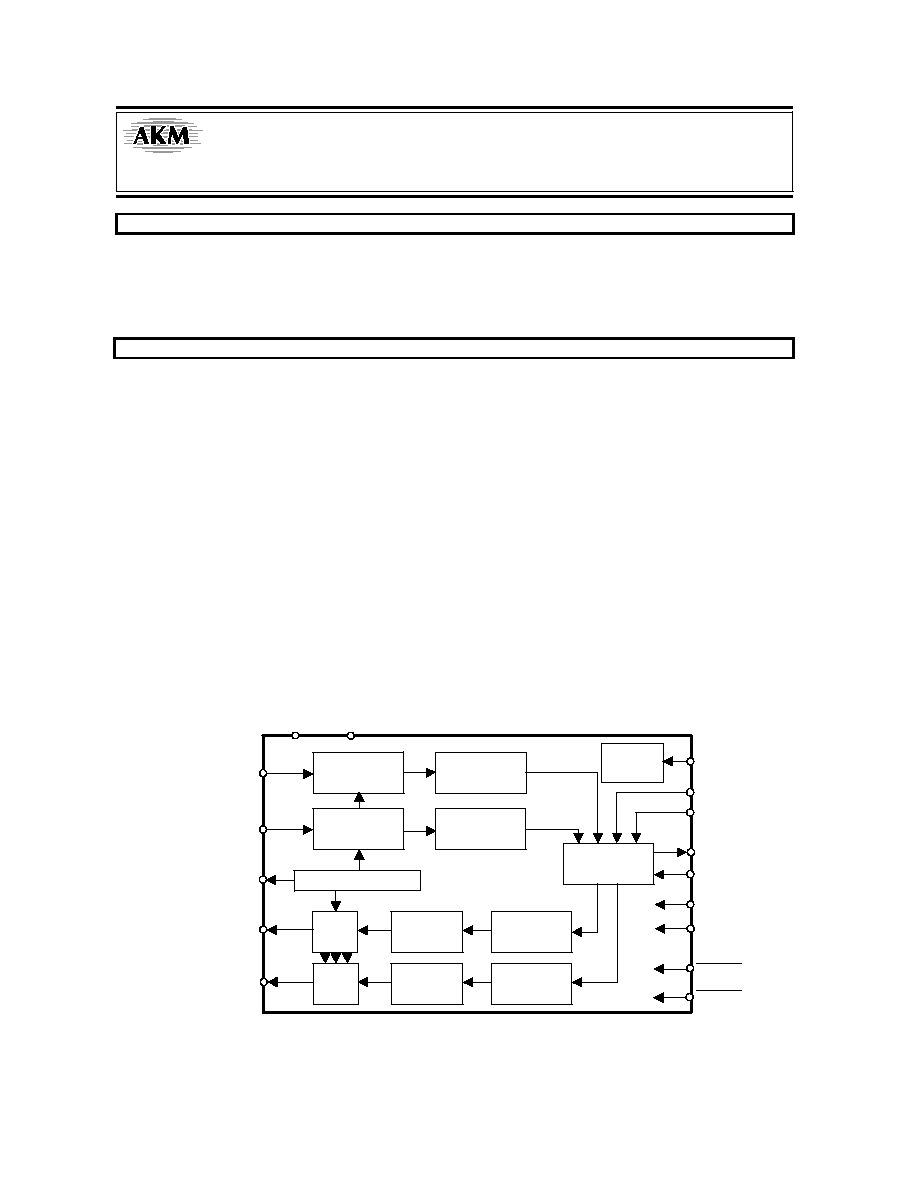
GENERAL DESCRIPTION
The AK4550 is a low voltage 16bit A/D & D/A converter for portable digital audio system. In the AK4550,
the loss of accuracy form clock jitter is also improved by using SCF techniques for on-chip post filter.
Analog signal input/output of the AK4550 are single-ended, therefore, any external filters are not required.
The AK4550 is suitable for portable digital audio system, as the AK4550 is lower power dissipation and a
smaller package than AK4518.
FEATURES
o
HPF for DC-offset cancel (fc=3.4Hz)
o
Single-ended ADC
- S/(N+D): 82dB@VDD=2.5V
- Dynamic Range, S/N: 89dB@VDD=2.5V
o
Single-ended DAC
- Digital de-emphasis for 32kHz, 44.1kHz, 48kHz sampling
- S/(N+D): 85dB@VDD=2.5V
- Dynamic Range, S/N: 92dB@VDD=2.5V
o
Audio I/F format: MSB First, 2's Compliment (AK4518 compatible)
- ADC: 16bit MSB justified
- DAC: 16bit LSB justified
o
Input/Output Voltage: 0.6 X VDD (=1.5Vpp@VDD=2.5V)
o
High Jitter Tolerance
o
Sampling Rate: 8kHz to 50kHz
o
Master Clock: 256fs or 384fs or 512fs
o
Power Supply: 2.3 to 3.6V
o
Low Power Supply Current: 10mA
o
Ta = -40 to 85∞C
o
Very Small Package: 16pin TSSOP
Modulator
MCLK
VDD
VSS
AOUTL
AINL
LRCK
SCLK
VCOM
AINR
Modulator
Decimation
Filter
Serial I/O
Interface
Common Voltage
SDTO
Decimation
Filter
SDTI
PWDA
DEM0
PWAD
Clock
Divider
AOUTR
8X
Interpolator
8X
Interpolator
Modulator
Modulator
LPF
LPF
DEM1
Low Power & Small Package 16bit
CODEC
AK4550
ASAHI KASEI
[AK4550]
M0068-E-01
2000/4
- 2 -
n
Ordering Guide
AK4550VT
-40
+85
∞
C
16pin TSSOP (0.65mm pitch)
AKD4550
Evaluation Board for AK4550
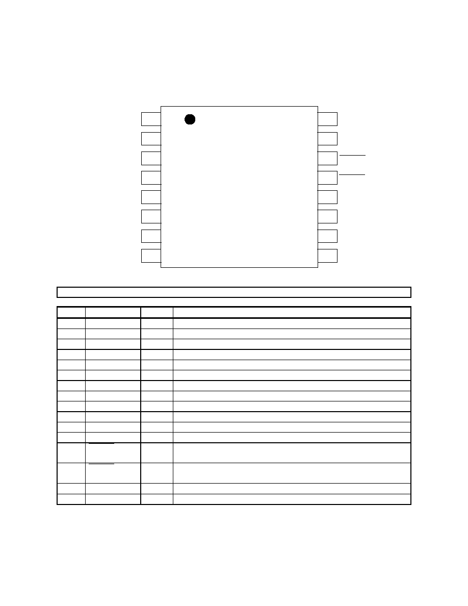
n
Pin Layout
1
VCOM
AINR
VSS
AINL
VDD
DEM0
DEM1
SDTO
Top
View
2
3
4
5
6
7
8
AOUTR
AOUTL
PWAD
SCLK
MCLK
LRCK
SDTI
16
15
14
13
12
11
10
9
PWDA
PIN/FUNCTION
No.
Pin Name
I/O
Function
1
VCOM
O
Common Voltage Output Pin, 0.45 x VDD
2
AINR
I
Rch Analog Input Pin
3
AINL
I
Lch Analog Input Pin
4
VSS
-
Ground Pin
5
VDD
-
Power Supply Pin
6
DEM0
I
De-emphasis Control Pin
7
DEM1
I
De-emphasis Control Pin
8
SDTO
O
Audio Serial Data Output Pin
9
SDTI
I
Audio Serial Data Input Pin
10
LRCK
I
Input/Output Channel Clock Pin
11
MCLK
I
Master Clock Input Pin
12
SCLK
I
Audio Serial Data Clock Pin
13
PWAD
I
ADC Power-Down & Reset Mode Pin
"L": Power down. ADC should always be reset upon power-up.
14
PWDA
I
DAC Power-Down & Reset Mode Pin
"L": Power down. DAC should always be reset upon power-up.
15
AOUTL
O
Lch Analog Output Pin
16
AOUTR
O
Rch Analog Output Pin
ASAHI KASEI
[AK4550]
M0068-E-01
2000/4
- 3 -
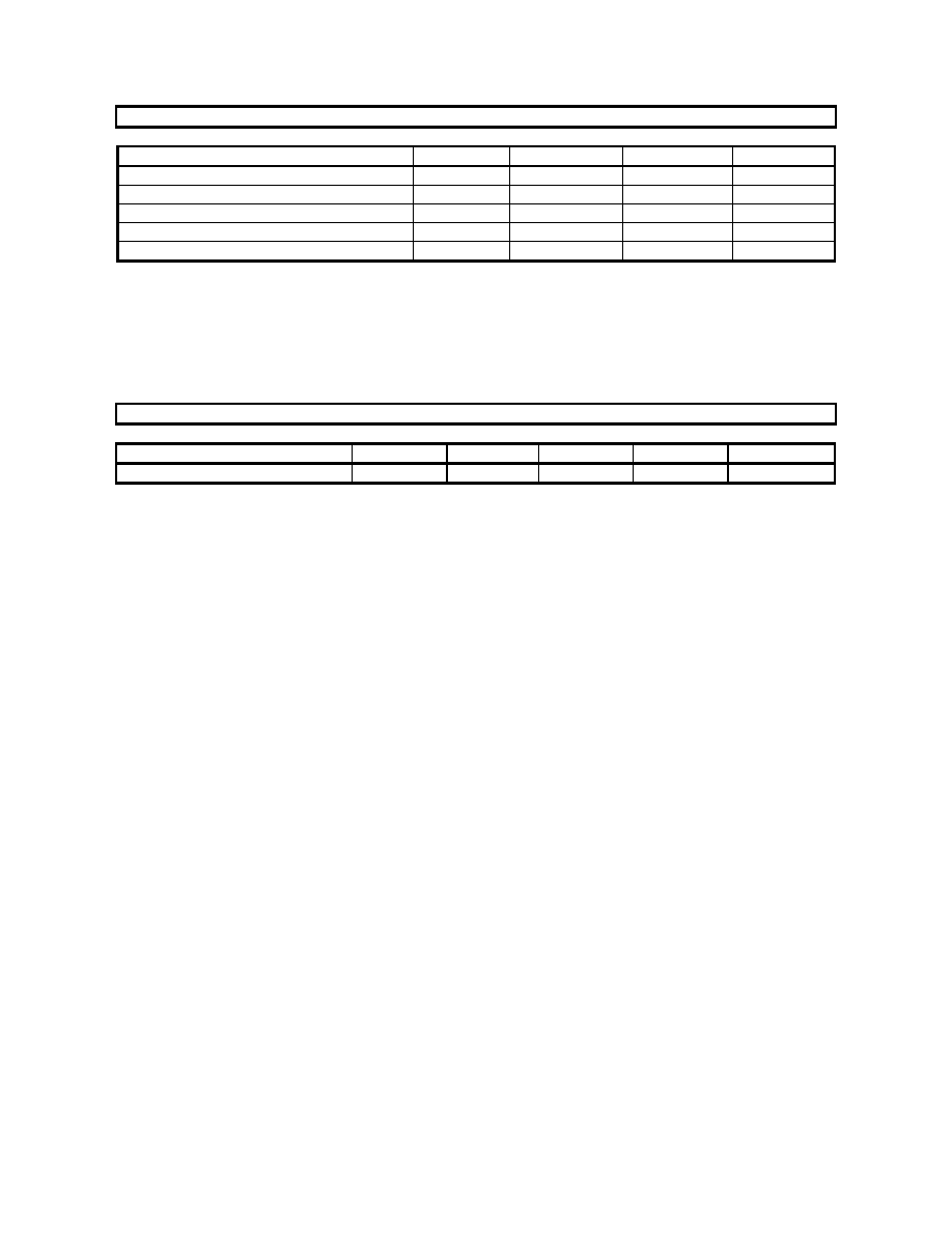
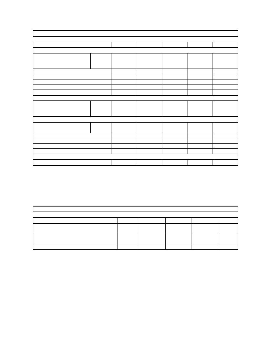
ABSOLUTE MAXIMUM RATINGS
(VSS=0V; Note 1)
Parameter
Symbol
min
max
Units
Power Supply
VDD
-0.3
4.6
V
Input Current (Any Pin Except Supplies)
IIN
-
±
10
mA
Input Voltage
VIN
-0.3
VDD+0.3
V
Ambient Temperature (power applied)
Ta
-40
85
∞
C
Storage Temperature
Tstg
-65
150
∞
C
Note:1. All voltages with respect to ground.
WARNING: Operation at or beyond these limits may results in permanent damage to the device.
Normal operation is not guaranteed at these extremes.
RECOMMENDED OPERATING CONDITIONS
(VSS=0V; Note 1)
Parameter
Symbol
min
typ
max
Units
Power Supply
VDD
2.3
2.5
3.6
V
Note:1. All voltages with respect to ground.
*AKM assumes no responsibility for the usage beyond the conditions in this data sheet.
ASAHI KASEI
[AK4550]
M0068-E-01
2000/4
- 4 -
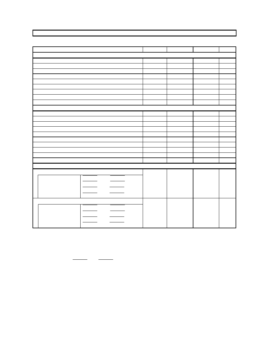
ANALOG CHARACTERISTICS
(Ta=25
∞
C; VDD=2.5V; fs=44.1kHz; Signal Frequency=1kHz; SCLK=64fs; Measurement frequency=10Hz
20kHz;
unless otherwise specified)
Parameter
min
typ
max
Units
ADC Analog Input Characteristics: Analog Source Impedance=470
(Note 2)
Resolution
16
Bits
S/(N+D) (-0.5dB Input)
72
82
dB
D-Range (-60dB Input, A-weighted)
82
89
dB
S/N (A-weighted)
82
89
dB
Interchannel Isolation
80
95
dB
Interchannel Gain Mismatch
0.2
0.5
dB
Input Voltage (Note 3)
1.35
1.50
1.65
Vpp
Input Resistance
50
100
k
Power Supply Rejection (Note 4)
35
dB
DAC Analog Output Characteristics: (Note 5)
Resolution
16
Bits
S/(N+D)
75
85
dB
D-Range (-60dB Output, A-weighted)
86
92
dB
S/N (A-weighted)
86
92
dB
Interchannel Isolation
80
95
dB
Interchannel Gain Mismatch
0.2
0.5
dB
Output Voltage (Note 3)
1.35
1.50
1.65
Vpp
Load Resistance
10
k
Load Capacitance
30
pF
Power Supply Rejection (Note 4)
50
dB
Power Supplies
Power Supply Current
AD+DA
AD
DA
Power down (Note 6)
PWAD = "H", PWDA = "H"
PWAD = "H", PWDA = "L"
PWAD = "L", PWDA = "H"
PWAD = "L", PWDA = "L"
10
5.6
5.6
10
15
8.4
8.4
50
mA
mA
mA
uA
Power Consumption
AD+DA
AD
DA
Power down (Note 6)
PWAD = "H", PWDA = "H"
PWAD = "H", PWDA = "L"
PWAD = "L", PWDA = "H"
PWAD = "L", PWDA = "L"
25
14
14
25
37.5
21
21
125
mW
mW
mW
uW
Notes: 2. The offset of ADC is removed by internal HPF.
3. Input /Output of ADC and DAC scales with VDD voltage. 0.6 X VDD(typ).
4. PSR is applied to VDD with 1kHz, 50mV.
5. Measured by AD725C (SHIBASOKU). RMS mode.
6. In case of power-down mode, all digital input including clocks pins (MCLK, SCLK, LRCK) are held VDD
or VSS. But PWAD and PWDA pins are held VSS.
ASAHI KASEI
[AK4550]
M0068-E-01
2000/4
- 5 -
FILTER CHARACTERISTICS
(Ta=25
∞
C; VDD=2.3
3.6V; fs=44.1kHz; DEM0="1", DEM1="0")
Parameter
Symbol
min
typ
max
Units
ADC Digital Filter (Decimation LPF):
Passband (Note 7)
±
0.1dB
-1.0dB
-3.0dB
PB
0
20.0
21.1
17.4
kHz
kHz
kHz
Stopband
SB
27.0
kHz
Passband Ripple
PR
±
0.1
dB
Stopband Attenuation
SA
65
dB
Group Delay (Note 8)
GD
17.0
1/fs
Group Delay Distortion
GD
0
us
ADC Digital Filter (HPF):
Frequency Response (Note 7)
-3dB
-0.5dB
-0.1dB
FR
3.4
10
22
Hz
Hz
Hz
DAC Digital Filter:
Passband (Note 7)
±
0.1dB
-6.0dB
PB
0
22.05
20.0
kHz
kHz
Stopband
SB
24.1
kHz
Passband Ripple
PR
±
0.06
dB
Stopband Attenuation
SA
43
dB
Group Delay (Note 8)
GD
14.8
1/fs
DAC Digital Filter + Analog Filter
Frequency Response 0
20.0kHz
FR
±
0.5
dB
Notes: 7. The passband and stopband frequencies scale with fs (sampling frequency).
For examples, PB=20.0kHz(@ADC: -1.0dB, DAC: -0.1dB) are 0.454 x fs.
8. The calculating delay time which occurred by digital filtering. This time is from the input of analog signal to
setting the 16bit data of both channels to the output register for ADC. For DAC, this time is from setting the
16bit data of both channels on input register to the output of analog signal.
DC CHARACTERISTICS
(Ta=25
∞
C; VDD=2.3
3.6V)
Parameter
Symbol
min
typ
max
Units
High-Level Input Voltage
Low-Level Input Voltage
VIH
VIL
70
%
VDD
-
-
-
-
30
%
VDD
V
V
High-Level Output Voltage (Iout=-20uA)
Low-Level Output Voltage (Iout=20uA)
VOH
VOL
VDD-0.1
-
-
-
0.1
V
V
Input Leakage Current
Iin
-
-
±
10
uA