
ASAHI KASEI
[AKD4555-E]
<KM078200>
2005/03
- 1 -
GENERAL DESCRIPTION
AKD4555-E is an evaluation board for the portable digital audio 16bit A/D and D/A converter, AK4555.
The AKD4555-E can evaluate A/D converter and D/A converter separately in addition to loopback mode
(A/D
D/A). The A/D section can be evaluated by interfacing with AKM's DAC evaluation boards directly.
The AKD4555-E has the interface with AKM's ADC evaluation boards. Therefore, it's easy to evaluate the
D/A section. The AKD4555-E also has the digital audio interface and can achieve the interface with digital
audio systems via opt-connector.
Ordering guide
AKD4555
-E
---
Evaluation
board
for
AK4555
FUNCTION
�
Compatible with 2 types of interface
- Direct interface with AKM's A/D & D/A converter evaluation boards
-
DIT/DIR
with
optical
input/output
AK4555
REG
VDD
Regulator
AGND
DGND
AINL/
AINR
AOUTL/
AOUTR
AK4114
DIT/DIR
10pin Header
DSP
Opt Out
Opt In
Figure 1. AKD4555-E Block Diagram
* Circuit diagram and PCB layout are attached at the end of this manual.
Evaluation board Rev.0 for AK4555
AKD4555-E

ASAHI KASEI
[AKD4555-E]
<KM078200>
2005/03
- 2 -
Evaluation Board Manual
Operation sequence
1) Set up the power supply lines.
[VDD]
(Orange) =
1.6
3.6V : for VDD of AK4555
[REG] (Red) = 5.0V : for regulator
[AGND] (Black) = 0V : for analog ground (including VSS of AK4555)
[DGND] (Black) = 0V : for logic ground
Each supply line should be distributed from the power supply unit.
2) Set up the evaluation mode, jumper pins and DIP switches.
(See the followings.)
3) Power on.
The AK4555 should be reset once bringing SW2 (PDN) "OFF" upon power-up.

ASAHI KASEI
[AKD4555-E]
<KM078200>
2005/03
- 3 -
Evaluation mode
Applicable
Evaluation
Mode
1) Evaluation of loopback mode (default)
2) Evaluation of D/A using A/D converted data
3) Evaluation of D/A using DIR (Optical Link)
4) Evaluation of A/D using D/A converted data
5) Evaluation of A/D using DIT (Optical Link)
6) All interface signals including master clock are fed externally.
DIT
PORT2
PORT3
DIR
AKD53XX
A/D Board
AKD43XX
D/A Board
PORT1
AKD4555-E
1)
2)
3)
4)
5)
CD Player
10pin-Header
1) Evaluation of loopback mode. (default)
Nothing should be connected to PORT1/PORT3.
JP4
MCLK
JP5
SCLK
JP7
SDTI
JP6
LRCK
ADC
DIR

ASAHI KASEI
[AKD4555-E]
<KM078200>
2005/03
- 4 -
2) Evaluation of D/A using A/D converted data.
D/A part can be evaluated by connecting with AKM's A/D evaluation boards via PORT3.
Nothing should be connected to PORT1
JP4
MCLK
JP5
SCLK
JP7
SDTI
JP6
LRCK
ADC
DIR
3) Evaluation of D/A using DIR. (Optical link)
PORT1 (TORX141) is used. DIR generates MCLK, SCLK, LRCK and SDATA from the received data
through optical connector (TORX141). Used for the evaluation using CD test disk. Nothing should be
connected to PORT2/PORT3.
JP4
MCLK
JP5
SCLK
JP7
SDTI
JP6
LRCK
ADC
DIR
4) Evaluation of A/D using D/A converted data.
A/D part can be evaluated by connecting with AKM's D/A evaluation boards via PORT3.
Nothing should be connected to PORT1.
JP4
MCLK
JP5
SCLK
JP7
SDTI
JP6
LRCK
ADC
DIR
ASAHI KASEI
[AKD4555-E]
<KM078200>
2005/03
- 5 -
5) Evaluation of A/D using DIT. (Optical link)
PORT2 (TOTX141) is used. DIT generates audio bi-phase signal from received data and which is output
through optical connector (TOTX141). It is possible to connect AKM's D/A converter evaluation boards
on the digital-amplifier, which equips DIR input.
JP4
MCLK
JP5
SCLK
JP7
SDTI
JP6
LRCK
ADC
DIR
6) All interfacing signals (MCLK, SCLK, LRCK) are fed from the external circuit through PORT3.
Under the following set-up, all external signals needed for the AK4555 to operate could be fed through
PORT3.
JP4
MCLK
JP5
SCLK
JP7
SDTI
JP6
LRCK
ADC
DIR

ASAHI KASEI
[AKD4555-E]
<KM078200>
2005/03
- 6 -
DIP switch set up
Upper-side is "ON" ("H") and lower side is "OFF" ("L").
[SW1]: Set up the AK4555 and AK4114.
.
SW No.
SW Name
Mode
1 DIF2,
0
AK45545and AK4114 Audio Format Setting
Always ON.
2
DEM1
Set up the de-emphasis of AK4555
3
DEM0
(See table 2)
4 NC
No
use
Table 1. DIPswitch set-up of AK4114
DEM1
(SW1-#2)
DEM0
(SW1-#3)
Mode
OFF
OFF
44.1kHz
OFF
ON
OFF
ON OFF 48kHz
ON ON 32kHz
Table 2. DIPswitch set up of de-emphasis

ASAHI KASEI
[AKD4555-E]
<KM078200>
2005/03
- 7 -
Other jumper pins set up
[JP1] (GND): Connection between AGND and DGND
open:
Both
grounds
are
separated on board.<default>
short: Both grounds are connected on board.
[JP2]
(REG):
Select to regulator
open: On-board regulator is not used. <default>
short: On-board
regulator
is
used.(The connector "VDD" can be open.)
[JP3] (PWR): Pull up power supply select for SDTO.
VDD: Connected to VDD of AK4555. <default>
D3V:
Supplied
from
regulator
(3V).
The function of the toggle SW.
Upper-side is "ON" and lower side is "OFF".
[SW2] (PDN): Resets the AK4555 and AK4114. Keep "ON" during normal operation.
Indication for LED
[LED1] (ERF): Monitor INT0 pin of the AK4114. LED turns on when some error has occurred to AK4114.

ASAHI KASEI
[AKD4555-E]
<KM078200>
2005/03
- 8 -
Input Circuit
R20
560
+
C28
4.7u
R21
560
+
C29
4.7u
6
4
3
J1
AINL/AINR
AINR
AINL
Figure 2. Input circuit on board
Output Circuit
R22
10k
R23
10k
R24
220
R25
220
+
C30
22u
+
C31
22u
6
4
3
J2
AOUTL/AOUTR
AOUTR
AOUTL
Figure 3. Output circuit on board
* AKM assumes no responsibility for the trouble when using the circuit examples.

ASAHI KASEI
[AKD4555-E]
<KM078200>
2005/03
- 9 -
MEASUREMENT RESULTS
[Measurement condition]
� Measurement unit : Audio Precision, System two
�
MCLK :
256fs
� SCLK : 64fs
� fs : 44.1kHz
�
Bit
:
16bit
� Power Supply : VDD = VP = 2.5V, VD = 5V
�
Interface
:
DIT/DIR
�
Temperature :
Room
1. ADC
VDD Parameter
Measured
Filter AINL AINR
S/(N+D) (-0.5dBFS)
20kHz LPF
80.9 dB
81.0 dB
D-Range (-60dBFS)
20kLPF + A-weighted
89.4 dB
89.2 dB
2.5V
S/N (0 data)
20kLPF + A-weighted
89.3 dB
89.2 dB
2. DAC
VDD Parameter
Measured
Filter AOUTL
AOUTR
S/(N+D) (0dBFS)
20kHz LPF
84.5 dB
84.5 dB
D-Range (-60dBFS)
22kLPF + A-weighted
91.6 dB
91.7 dB
2.5V
S/N (0 data)
22kLPF + A-weighted
91.9 dB
92.1 dB
ASAHI KASEI
[AKD4555-E]
<KM078200>
2005/03
- 10 -
3.PLOT DATA
3-1 ADC
AKM
AK4554 ADC THD+N vs.Input Level
VDD=2.5V, fs=44.1kHz, fin=1kHz
-90
-60
-88
-86
-84
-82
-80
-78
-76
-74
-72
-70
-68
-66
-64
-62
d
B
F
S
-120
-10
-110
-100
-90
-80
-70
-60
-50
-40
-30
-20
dBr
Fig. 1 THD+N vs. Input Level
AKM
AK4554 ADC THD+N vs. Input Frequency
VDD=2.5V, fs=44.1kHz, Input Level=-0.5dB
-90
-60
-88
-86
-84
-82
-80
-78
-76
-74
-72
-70
-68
-66
-64
-62
d
B
F
S
20
20k
50
100
200
500
1k
2k
5k
10k
Hz
Fig.2 THD+N vs. Input Frequency
ASAHI KASEI
[AKD4555-E]
<KM078200>
2005/03
- 11 -
AKM
AK4554 ADC Linearity
VDD=2.5V, fs=44.1kHz, fin=1kHz
-110
+0
-100
-90
-80
-70
-60
-50
-40
-30
-20
-10
d
B
F
S
-110
+0
-100
-90
-80
-70
-60
-50
-40
-30
-20
-10
dBr
Fig.3 Linearity
AKM
AK4554 ADC Frequency Response
VDD=2.5V, fs=44.1kHz, Input level=-0.5dB
-3
+0
-2.8
-2.6
-2.4
-2.2
-2
-1.8
-1.6
-1.4
-1.2
-1
-0.8
-0.6
-0.4
-0.2
d
B
F
S
20
20k
50
100
200
500
1k
2k
5k
10k
Hz
Fig.4 Frequency Response

ASAHI KASEI
[AKD4555-E]
<KM078200>
2005/03
- 12 -
AKM
AK4554 ADC FFT Plot
VDD=2.5V, fs=44.1kHz, fin=1kHz, Input Level=-0.5dB
20
20k
50
100
200
500
1k
2k
5k
10k
Hz
-160
+0
-150
-140
-130
-120
-110
-100
-90
-80
-70
-60
-50
-40
-30
-20
-10
d
B
F
S
Fig.5 FFT Plot (Input Level = -0.5dB)
AKM
AK4554 ADC FFT Plot
VDD=2.5V, fs=44.1kHz, fin=1kHz, Input Level=-60dB
20
20k
50
100
200
500
1k
2k
5k
10k
Hz
-160
+0
-150
-140
-130
-120
-110
-100
-90
-80
-70
-60
-50
-40
-30
-20
-10
d
B
F
S
Fig.6 FFT Plot (Input Level = -60dB)

ASAHI KASEI
[AKD4555-E]
<KM078200>
2005/03
- 13 -
AKM
AK4554 ADC FFT
VDD=2.5V, fs=44.1kHz, Input Level=-0.5dB
20
20k
50
100
200
500
1k
2k
5k
10k
Hz
-160
+0
-150
-140
-130
-120
-110
-100
-90
-80
-70
-60
-50
-40
-30
-20
-10
d
B
F
S
Fig.7 FFT Plot (no signal)
Fig.8 Crosstalk (red : L--->R, blue : R--->L)
ASAHI KASEI
[AKD4555-E]
<KM078200>
2005/03
- 14 -
3-2. DAC
AKM
AK4554 DAC THD+N vs. Input Level
VDD=2.5V, fs=44.1kHz, fin=1kHz
-120
+0
-110
-100
-90
-80
-70
-60
-50
-40
-30
-20
-10
dBFS
-100
-60
-98
-96
-94
-92
-90
-88
-86
-84
-82
-80
-78
-76
-74
-72
-70
-68
-66
-64
-62
d
B
r
A
Fig.9 THD+N vs. Input Level
AKM
AK4554 DAC THD+N vs. Input Frequency
VDD=2.5V, fs=44.1kHz, Input Level=0dB
20
20k
50
100
200
500
1k
2k
5k
10k
Hz
-100
-60
-98
-96
-94
-92
-90
-88
-86
-84
-82
-80
-78
-76
-74
-72
-70
-68
-66
-64
-62
d
B
r
A
Fig.10 THD+N vs. Input Frequency

ASAHI KASEI
[AKD4555-E]
<KM078200>
2005/03
- 15 -
AKM
AK4554 DAC Linearity
VDD=2.5V, fs=44.1kHz, fin=1kHz
-120
+0
-110
-100
-90
-80
-70
-60
-50
-40
-30
-20
-10
dBFS
-120
+0
-110
-100
-90
-80
-70
-60
-50
-40
-30
-20
-10
d
B
r
A
Fig.11 Linearity
AKM
AK4554 DAC Frequency Response
VDD=2.5V, fs=44.1kHz, Input Level=0dB
2k
20k
4k
6k
8k
10k
12k
14k
16k
18k
Hz
-1
+1
-0.9
-0.8
-0.7
-0.6
-0.5
-0.4
-0.3
-0.2
-0.1
+0
+0.1
+0.2
+0.3
+0.4
+0.5
+0.6
+0.7
+0.8
+0.9
d
B
r
A
Fig.12 Frequency Response

ASAHI KASEI
[AKD4555-E]
<KM078200>
2005/03
- 16 -
AKM
AK4554 DAC FFT Plot
VDD=2.5V, fs=44.1kHz,fin=1kHz, Input Level=0dB
20
20k
50
100
200
500
1k
2k
5k
10k
Hz
-160
+0
-150
-140
-130
-120
-110
-100
-90
-80
-70
-60
-50
-40
-30
-20
-10
d
B
r
A
Fig.13 FFT Plot (Input Level = 0dB)
AKM
AK4554 DAC FFT Plot
VDD=2.5V, fs=44.1kHz,fin=1kHz, Input Level=-60dB
20
20k
50
100
200
500
1k
2k
5k
10k
Hz
-160
+0
-150
-140
-130
-120
-110
-100
-90
-80
-70
-60
-50
-40
-30
-20
-10
d
B
r
A
Fig.14 FFT Plot (Input Level = -60dB)

ASAHI KASEI
[AKD4555-E]
<KM078200>
2005/03
- 17 -
AKM
AK4554 DAC FFT
VDD=2.5V, fs=44.1kHz, Input Level=0dB
20
20k
50
100
200
500
1k
2k
5k
10k
Hz
-160
+0
-150
-140
-130
-120
-110
-100
-90
-80
-70
-60
-50
-40
-30
-20
-10
d
B
r
A
Fig.15 FFT Plot (no data)
Fig.16 Crosstalk (red : L--->R, blue : R--->L)

ASAHI KASEI
[AKD4555-E]
<KM078200>
2005/03
- 18 -
AKM
AK4554 DAC out-band-noise
VDD=2.5V, fs=44.1kHz, Input=no data
-160
+0
-150
-140
-130
-120
-110
-100
-90
-80
-70
-60
-50
-40
-30
-20
-10
d
B
r
A
20
100k
50
100
200
500
1k
2k
5k
10k
20k
50k
Hz
Fig.17 Out band noise
ASAHI KASEI
[AKD4555-E]
<KM078200>
2005/03
- 19 -
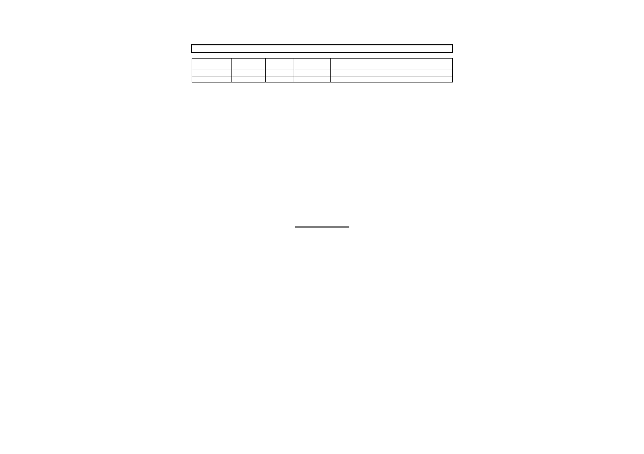
Revision History
Date
(YY/MM/DD)
Manual
Revision
Board
Revision
Reason Contents
05/03/31 KM078200 0 First
Edtion
IMPORTANT NOTICE
�
These products and their specifications are subject to change without notice. Before considering
any use or application, consult the Asahi Kasei Microsystems Co., Ltd. (AKM) sales office or
authorized distributor concerning their current status.
�
AKM assumes no liability for infringement of any patent, intellectual property, or other right in the
application or use of any information contained herein.
�
Any export of these products, or devices or systems containing them, may require an export license
or other official approval under the law and regulations of the country of export pertaining to customs
and tariffs, currency exchange, or strategic materials.
�
AKM products are neither intended nor authorized for use as critical components in any safety, life
support, or other hazard related device or system, and AKM assumes no responsibility relating to
any such use, except with the express written consent of the Representative Director of AKM. As
used here:
(a) A hazard related device or system is one designed or intended for life support or maintenance of
safety or for applications in medicine, aerospace, nuclear energy, or other fields, in which its
failure to function or perform may reasonably be expected to result in loss of life or in significant
injury or damage to person or property.
(b) A critical component is one whose failure to function or perform may reasonably be expected to
result, whether directly or indirectly, in the loss of the safety or effectiveness of the device or
system containing it, and which must therefore meet very high standards of performance and
reliability.
�
It is the responsibility of the buyer or distributor of an AKM product who distributes, disposes of, or
otherwise places the product with a third party to notify that party in advance of the above content
and conditions, and the buyer or distributor agrees to assume any and all responsibility and liability
for and hold AKM harmless from any and all claims arising from the use of said product in the
absence of such notification.

A
A
B
B
C
C
D
D
E
E
E
E
D
D
C
C
B
B
A
A
REG
VA
REG
VA
4554_SDTO
BCLK
MCLK
LRCK
SDTI
DEM1
DEM0
PWDAN
VD
LVC
VDD
Title
Size
Document Number
Rev
Date:
Sheet
of
AK4555
0
AKD4555-E
A3
1
4
Wednesday, March 02, 2005
Title
Size
Document Number
Rev
Date:
Sheet
of
AK4555
0
AKD4555-E
A3
1
4
Wednesday, March 02, 2005
Title
Size
Document Number
Rev
Date:
Sheet
of
AK4555
0
AKD4555-E
A3
1
4
Wednesday, March 02, 2005
DGND
AGND
(5V)
(1.6-3.6V)
OUT
IN
GND
T1
TA4803F
T1
TA4803F
+
C1
4.7u
+
C1
4.7u
R3
560
R3
560
R8
51
R8
51
C8
0.1u
C8
0.1u
R11 51
R11 51
1
REG
T45_R
REG
T45_R
1
2
L1
(short)
L1
(short)
+
C2
22u
+
C2
22u
JP2
REG
JP2
REG
R6
560
R6
560
R7
5.1
R7
5.1
+
C11
10u
+
C11
10u
R2
220
R2
220
R12 51
R12 51
C6
0.1u
C6
0.1u
6
4
3
J2
AOUTL/AOUTR
J2
AOUTL/AOUTR
R5
10k
R5
10k
+
C3
22u
+
C3
22u
R9
51
R9
51
JP1
GND
JP1
GND
+
C4
4.7u
+
C4
4.7u
1
VDD
T45_O
VDD
T45_O
1
2
+
C10
47u
+
C10
47u
1
DGND
T45_BK
DGND
T45_BK
6
4
3
J1
AINL/AINR
J1
AINL/AINR
R4
220
R4
220
VCOM
1
AINR
2
AINL
3
VSS
4
VDD
5
DEM0
6
DEM1
7
SDTO
8
LRCK
10
MCLK
11
SCLK
12
PWADN
13
AOUTL
15
PWDAN
14
AOUTR
16
SDTI
9
AK4555
U1
AK4555
U1
1
2
+
C7
47u
+
C7
47u
C5
0.1u
C5
0.1u
1
AGND
T45_BK
AGND
T45_BK
R1
10k
R1
10k
C9
0.1u
C9
0.1u
R10 51
R10 51
A
A
B
B
C
C
D
D
E
E
E
E
D
D
C
C
B
B
A
A
VD
4114_PDN
SDTO
DIR_SDTO
DIR_BICK
DIR_LRCK
DIR_MCKO
DEM0
DEM1
VD
VD
VD
VD
VD
VD
VD
VD
Title
Size
Document Number
Rev
Date:
Sheet
of
DIR/DIT
0
AKD4555-E
A3
2
4
Monday, February 07, 2005
Title
Size
Document Number
Rev
Date:
Sheet
of
DIR/DIT
0
AKD4555-E
A3
2
4
Monday, February 07, 2005
Title
Size
Document Number
Rev
Date:
Sheet
of
DIR/DIT
0
AKD4555-E
A3
2
4
Monday, February 07, 2005
DIF2,0
DEM 1
DEM 0
AK4555
AK4550/4
DIF2, 0
ON
OFF
DEM1
DEM0
OFF
OFF
OFF
ON
ON
OFF
ON
ON
44.1k
OFF
48k
32k
DIP SW
+
C13
10u
+
C13
10u
C16
0.47u
C16
0.47u
1
2
3
4
RP1
47k
RP1
47k
R15
1k
R15
1k
R16
5.1
R16
5.1
1
2
L2
47u
L2
47u
1
TP1 EXTCLK
TP1 EXTCLK
+
C21
10u
+
C21
10u
C18
5p
C18
5p
C15
0.1u
C15
0.1u
2
1
LED1
ERF
LED1
ERF
C19
0.1u
C19
0.1u
C20
0.1u
C20
0.1u
OUT
1
VCC
3
GND
2
PORT1
TORX141
PORT1
TORX141
+
C14
10u
+
C14
10u
C12
0.1u
C12
0.1u
1
2
X1
11.2896MHz
X1
11.2896MHz
C17
5p
C17
5p
R13
470
R13
470
C23
0.1u
C23
0.1u
IPS0
1
NC
2
DIF0
3
TEST2
4
DIF1
5
NC
6
DIF2
7
IPS1
8
P/SN
9
XTL0
10
XTL1
11
TVD
D
13
D
VSS
14
TX0
15
TX1
16
BO
U
T
17
COUT
18
UOUT
19
VO
U
T
20
DV
DD
21
D
VSS
22
MC
KO1
23
BICK
26
MCKO2
27
DAUX
28
XTO
29
XTI
30
PDN
31
CM0
32
CM1
33
OCKS1
34
OCKS0
35
INT0
36
AVD
D
38
R
39
VC
O
M
40
AVSS
41
RX
0
42
NC
43
RX
1
44
TEST1
45
RX
2
46
NC
47
RX
3
48
VIN
12
LRCK
24
SDTO
25
IN
T1
37
U2
AK4114
U2
AK4114
GND
1
VCC
2
IN
3
PORT2
TOTX141
PORT2
TOTX141
+
C22
10u
+
C22
10u
R14
18k
R14
18k
1
2
3
6
5
4
SW1
MODE2
SW1
MODE2
1
2
14
7
U3A
74HC14
U3A
74HC14

A
A
B
B
C
C
D
D
E
E
E
E
D
D
C
C
B
B
A
A
LRCK
DIR_SDTO
MCLK
SDTO
BCLK
SDTI
LVC
4114_PDN
PWDAN
DIR_MCKO
DIR_BICK
DIR_LRCK
4554_SDTO
SDTO
VD
VD
VD
LVC
VD
VD
LVC
VDD
Title
Size
Document Number
Rev
Date:
Sheet
of
LOGIC
0
AKD4555-E
A3
3
4
Monday, February 07, 2005
Title
Size
Document Number
Rev
Date:
Sheet
of
LOGIC
0
AKD4555-E
A3
3
4
Monday, February 07, 2005
Title
Size
Document Number
Rev
Date:
Sheet
of
LOGIC
0
AKD4555-E
A3
3
4
Monday, February 07, 2005
VD
DIR
BICK
ADC
SDTI
MCLK
LRCK
L
H
for
74LVC07ANS
for
74HC14
GND
GND
NC
NC
SDTO
VDD
D3V
5
6
14
7
U3C
74HC14
U3C
74HC14
1
2
3
4
5
6
7
8
9
10
PORT3
DSP
PORT3
DSP
JP6LRCK
JP6LRCK
2
1
D1
1S1588
D1
1S1588
A1
2
A2
3
A3
4
A4
5
A5
6
A6
7
A7
8
A8
9
G1
1
G2
19
Y1
18
Y2
17
Y3
16
Y4
15
Y5
14
Y6
13
Y7
12
Y8
11
VCC
20
GND
10
U4
74LVC541
U4
74LVC541
C27
0.1u
C27
0.1u
2
1
3
SW2
PDN
SW2
PDN
R19
10k
R19
10k
C24
0.1u
C24
0.1u
JP5SCLK
JP5SCLK
JP7
SDTI
JP7
SDTI
R18
10k
R18
10k
R17
1k
R17
1k
3
4
14
7
U3B
74HC14
U3B
74HC14
JP3 PWR
JP3 PWR
C25
0.1u
C25
0.1u
1
2
14
7
U5A
74LVC07ANS
U5A
74LVC07ANS
C26
0.1u
C26
0.1u
JP4MCLK
JP4MCLK

A
A
B
B
C
C
D
D
E
E
E
E
D
D
C
C
B
B
A
A
VD
LVC
Title
Size
Document Number
Rev
Date:
Sheet
of
PIN
0
AKD4555-E
A3
4
4
Monday, February 07, 2005
Title
Size
Document Number
Rev
Date:
Sheet
of
PIN
0
AKD4555-E
A3
4
4
Monday, February 07, 2005
Title
Size
Document Number
Rev
Date:
Sheet
of
PIN
0
AKD4555-E
A3
4
4
Monday, February 07, 2005
13
12
14
7
U5F
74LVC07ANS
U5F
74LVC07ANS
5
6
14
7
U5C
74LVC07ANS
U5C
74LVC07ANS
3
4
14
7
U5B
74LVC07ANS
U5B
74LVC07ANS
11
10
14
7
U3E
74HC14
U3E
74HC14
11
10
14
7
U5E
74LVC07ANS
U5E
74LVC07ANS
9
8
14
7
U3D
74HC14
U3D
74HC14
9
8
14
7
U5D
74LVC07ANS
U5D
74LVC07ANS
13
12
14
7
U3F
74HC14
U3F
74HC14


