ASAHI KASEI
[AKD4631-VN]
<KM077301>
2005/01
- 1 -
GENERAL DESCRIPTION
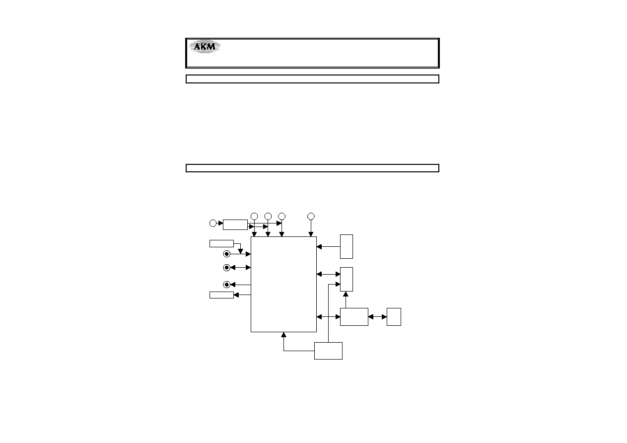
AKD4631-VN is an evaluation board for the AK4631VN, 16bit mono CODEC with MIC/SPK amplifier. The
AKD4631-VN can evaluate A/D converter and D/A converter separately in addition to loopback mode
(A/D
D/A). AKD4631-VN also has the digital audio interface and can achieve the interface with digital
audio systems via opt-connector.
Ordering guide
AKD4631-VN --- Evaluation board for AK4631VN
(Cable for connecting with printer port of IBM-AT, compatible PC and control
software are packed with this. This control software does not support Windows NT.)
FUNCTION
∑
DIT/DIR with optical input/output
∑
BNC connector for an external clock input
∑
10pin Header for serial control mode
10pin Header
Control Data
10pin Header
GND
BEEP/MIN/MOUT
AK4114
Opt In
Opt Out
Clock
Gen
AK4631VN
SVDD
AVDD
DSP
DVDD
MIC-Jack
SPK-Jack
AOUT
MIC
5V
Regulator
3.3V
Figure 1. AKD4631-VN Block Diagram
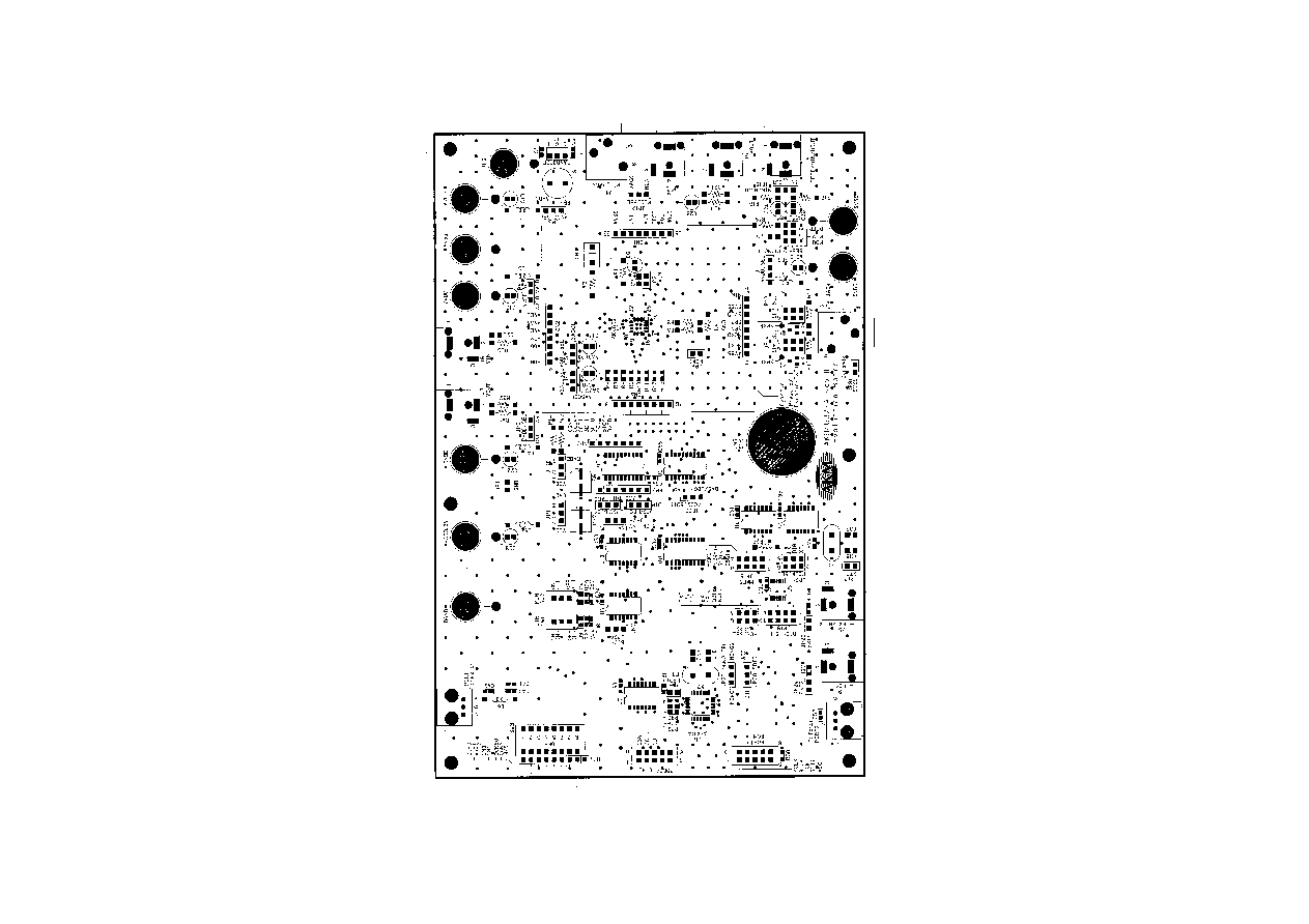
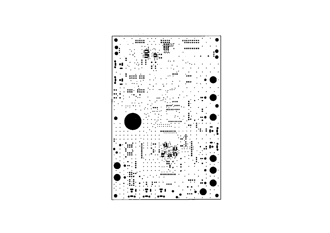
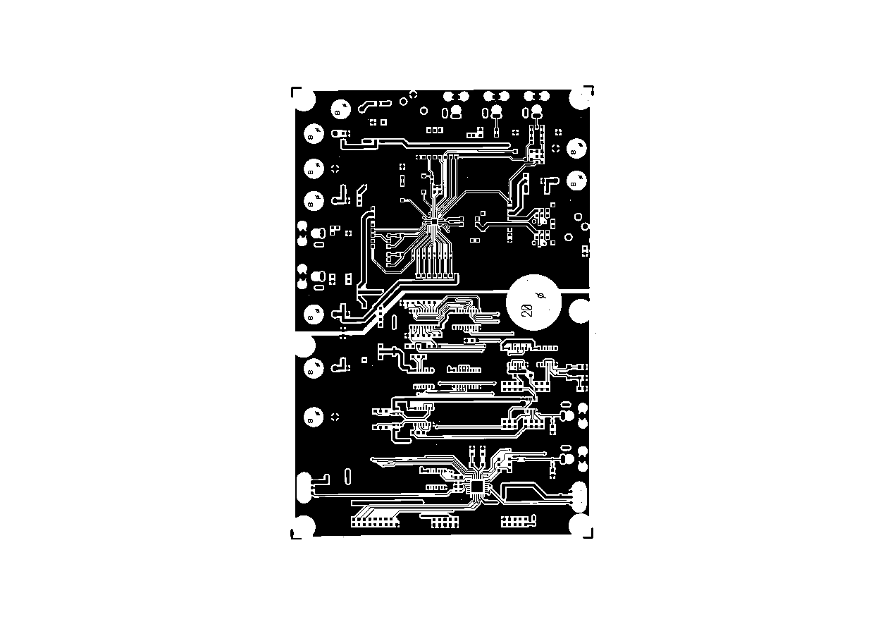
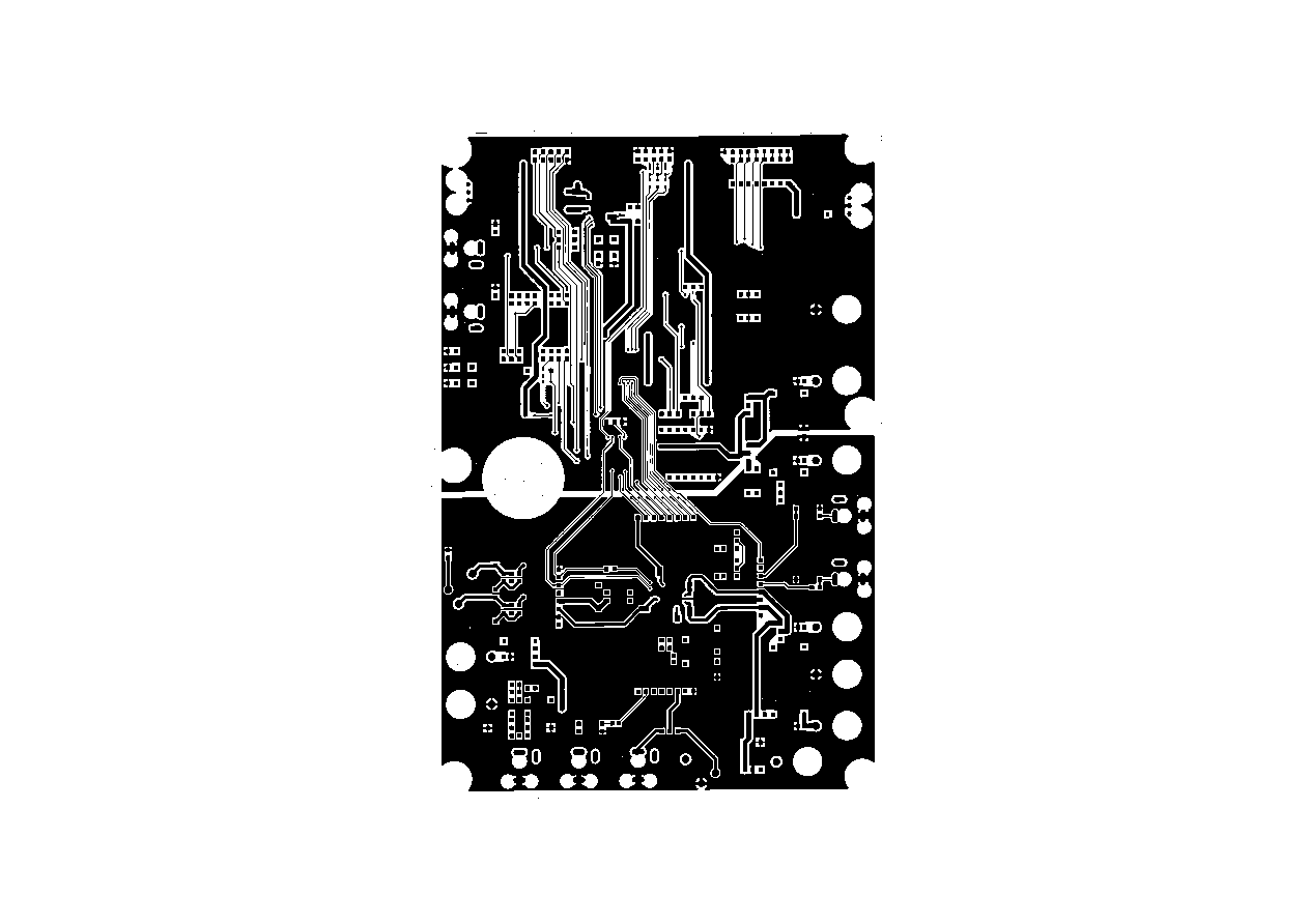
* Circuit diagram and PCB layout are attached at the end of this manual.
AK4631-VN Evaluation board Rev.0
AKD4631-VN

ASAHI KASEI
[AKD4631-VN]
<KM077301>
2005/01
- 2 -
Evaluation Board Manual
Operation sequence
1) Set up the power supply lines.
1-1) When AVDD, DVDD, SVDD, and VCC are supplied from the regulator. (AVDD, DVDD, SVDD, and
VCC jack should be open.). See "
Other jumper pins set up
(page 10)". <default>
[REG] (red
)
=
5V
[AVDD] (orange) = open : 3.3V is supplied to AVDD of AK4631-VN from regulator.
[DVDD] (orange) = open : 3.3V is supplied to DVDD of AK4631-VN from regulator.
[SVDD] (blue) = open : 3.3V is supplied to SVDD of AK4631-VN from regulator.
[VCC] (orenge) = open : 3.3V is supplied to logic block from regulator.
[AVSS]
(black)
=
0V
:
for
analog
ground
[AGND] (black)
=
0V
:
for
analog
ground
[DGND] (black)
=
0V
:
for
logic
ground
1-2) When AVDD, DVDD, SVDD, and VCC are not supplied from the regulator. (AVDD, DVDD, SVDD, and
VCC jack should be junction.) See "
Other jumper pins set up
(page 10)".
[REG] (red) = "REG" jack should be open.
[AVDD] (orange) =
2.6
3.6V : for AVDD of AK4631-VN (typ. 3.3V)
[DVDD] (orange) =
2.6
3.6V : for DVDD of AK4631-VN (typ. 3.3V)
[SVDD]
(blue) =
2.6
5.25V : for SVDD of AK4631-VN (typ. 3.3V, 5.0V)
[VCC] (orenge) =
2.6
3.6V : for logic (typ. 3.3V)
[AVSS]
(black)
=
0V
:
for
analog
ground
[AGND] (black)
=
0V
:
for
analog
ground
[DGND] (black)
=
0V
:
for
logic
ground
Each supply line should be distributed from the power supply unit.
AVDD and DVDD must be same voltage level.
2) Set up the evaluation mode, jumper pins and DIP switches.
(See the followings.)
3) Power on.
The AK4631VN and AK4114 should be reset once bringing SW1, 2 "L" upon power-up.
Evaluation mode
In case of AK4631VN evaluation using AK4114, it is necessary to correspond to audio interface format for
AK4631VN and AK4114. About AK4631VN's audio interface format, refer to datasheet of AK4631VN.
About AK4114's audio interface format, refer to Table 2 in this manual.
Applicable Evaluation Mode
(1) Evaluation of loop-back mode (A/D
D/A) : PLL, Master Mode (Default)
(2) Evaluation of loop-back mode (A/D
D/A) : PLL, Slave Mode (PLL Reference CLOCK: MCKI
pin)
(3) Evaluation of loop-back mode (A/D
D/A) : PLL, Slave Mode (PLL Reference CLOCK: BICK or
FCK pin)
(4) Evaluation of using DIR of AK4114 (opt-connector) : EXT, Slave Mode
(5)
Evaluation of using DIT of AK4114 (opt-connector) : EXT, Slave Mode
ASAHI KASEI
[AKD4631-VN]
<KM077301>
2005/01
- 3 -
(1) Evaluation of loop-back mode (A/D
D/A) : PLL, Master Mode (Default)
a) Set up jumper pins of MCKI clock
"MCKPD bit" in the AK4631-VN should be set to "0".
X'tal of 11.2896MHz, 12MHz, 12.288MHz, 13MHz, 24MHz or 27MHz can be set in X2. X'tal of 11.2896MHz
(Default) is set on the AKD4631-VN. Set "No.8 of SW3" to "H".
When an external clock (11.2896MHz, 12MHz, 12.288MHz, 13MHz, 24MHz or 27MHz) through a RCA
connector (J8: EXT/BICK) is supplied, select EXT on JP21 (MCLK_SEL) and short JP17 (XTE). JP23 (EXT1)
and R26 should be properly selected in order to much the output impedance of the clock generator.
b) Set up jumper pins of BICK clock
Output frequency (16fs/32fs/64fs) of BICK should be set by "BCKO1-0 bit" in the AK4631-VN.
There is no necessity for set up JP19.
c) Set up jumper pins of FCK clock
d) Set up jumper pins of DATA
When the AK4631VN is evaluated by loop-back mode (A/D
D/A), the jumper pins should be set to the
following.
JP17
XTE
MCLK_SEL
JP21
JP18
MKFS
256fs 512fs1024fs
XTL DIR EXT
MCKO
JP6
MCKI
JP22
FCK_SEL
2fs
EXT
JP28
FCK
ADC
DIR
1fs
JP26
4631_SDTI
ADC
DAC/LOOP
JP30
SDTI
DIR
ADC
JP29
JP20
BICK
JP27
BICK_INV
THR
INV
DIR ADC
BICK
THR
INV
BICK_SEL
JP19
EXT
16fs
32fs
64fs
ASAHI KASEI
[AKD4631-VN]
<KM077301>
2005/01
- 4 -
(2) Evaluation of loop-back mode (A/D
D/A) : PLL, Slave Mode (PLL Reference CLOCK: MCKI pin)
a) Set up jumper pins of MCKI clock
"MCKPD bit" in the AK4631VN should be set to "0".
X'tal of 11.2896MHz (Default) is set on the AKD4631-VN. In this case, the AK4631VN corresponds to PLL
reference clock of 12.2896MHz. In this evaluation mode, the output clock from MCKO-pin of the AK4631VN
is supplied to a divider (U3: 74VHC4040), BICK and FCK clocks are generated by the divider. Then "MCKO
bit" in the AK4631VN should be set to "1". When an external clock through a RCA connector (J8: EXT/BICK)
is supplied, select EXT on JP21 (MCLK_SEL) and short JP17 (XTE). JP23 (EXT1) and R26 should be properly
selected in order to match the output impedance of the clock generator.
b) Set up jumper pins of BICK clock
c) Set up jumper pins of FCK clock
d) Set up jumper pins of DATA
When the AK4631-VN is evaluated by loop-back mode (A/D
D/A), the jumper pins should be set to the
following.
JP17
XTE
MCLK_SEL
JP21
JP18
MKFS
256fs 512fs1024fs
XTL DIR EXT
MCKO
JP6
MCKI
JP28
FCK
ADC
DIR
JP22
FCK_SEL
2fs
EXT
1fs
JP26
4631_SDTI
ADC
DAC/LOOP
JP30
SDTI
DIR
ADC
JP29
JP20
BICK
JP27
BICK_INV
THR
INV
DIR ADC
BICK
THR
INV
BICK_SEL
JP19
EXT
16fs
32fs
64fs
ASAHI KASEI
[AKD4631-VN]
<KM077301>
2005/01
- 5 -
(3) Evaluation of loop-back mode (A/D
D/A) : PLL, Slave Mode (PLL Reference CLOCK: BICK or FCK
pin)
a) Set up jumper pins of MCKI clock
"MCKPD bit" in the AK4631VN should be set to "1". JP6 (MCKI) should be open.
b) Set up jumper pins of BICK clock
When an external clock through a RCA connector J8 (EXT/BICK) is supplied, select EXT on JP19
(MCLK_SEL) and short JP17 (XTE). JP23 (EXT1) and R26 should be properly selected in order to match the
output impedance of the clock generator.
In this evaluation mode, the selected clock from JP21 (MCLK_SEL) is supplied to a divider (U3: 74VHC4040),
BICK and FCK clocks are generated by the divider. Input frequency of master clock is set up in turn "256fs",
"512fs", "1024fs" from left.
And input frequency of BICK is set up in turn "16fs", "32fs", "64fs" from left.
JP17
XTE
MCLK_SEL
JP21
XTL DIR EXT
JP29
JP20
BICK
JP27
BICK_INV
THR
INV
DIR ADC
BICK
THR
INV
JP18
MKFS
256fs 512fs1024fs MCKO
JP18
MKFS
256fs 512fs1024fs MCKO
JP18
MKFS
256fs 512fs1024fs MCKO
BICK_SEL
JP19
EXT
16fs
32fs
64fs
BICK_SEL
JP19
EXT
16fs
32fs
64fs
BICK_SEL
JP19
EXT
16fs
32fs
64fs
ASAHI KASEI
[AKD4631-VN]
<KM077301>
2005/01
- 6 -
c) Set up jumper pins of FCK clock
When an external clock through a RCA connector J9 (FCK) is supplied, select EXT on JP22 (FCK_SEL). JP24
(EXT2) and R27 should be properly selected in order to match the output impedance of the clock generator.
d) Set up jumper pins of DATA
When the AK4631VN is evaluated by loop-back mode (A/D
D/A), the jumper pins should be set to the
following.
JP28
FCK
ADC
DIR
JP22
FCK_SEL
2fs
EXT
1fs
JP26
4631_SDTI
ADC
DAC/LOOP
JP30
SDTI
DIR
ADC
ASAHI KASEI
[AKD4631-VN]
<KM077301>
2005/01
- 7 -
(4) Evaluation of using DIR of AK4114 (opt-connector) : EXT, Slave Mode
a) Set up jumper pins of MCKI clock
"MCKPD bit" in the AK4631VN should be set to "0".
b) Set up jumper pins of BICK clock
c) Set up jumper pins of FCK clock
JP24 (EXT2) and R27 should be properly selected in order to match the output impedance of the clock generator.
d) Set up jumper pins of DATA
When D/A converter of the AK4631-VN is evaluated by using DIR of AK4114, the jumper pins should be set to
the following.
JP17
XTE
MCLK_SEL
JP21
XTL DIR EXT
JP6
MCKI
JP18
MKFS
256fs 512fs 1024fs
JP29
JP20
BICK
JP27
BICK_INV
THR
INV
DIR ADC
BICK
THR
INV
BICK_SEL
JP19
EXT
16fs
32fs
64fs
JP28
FCK
ADC
DIR
JP22
FCK_SEL
2fs
EXT
1fs
JP26
4631_SDTI
ADC
DAC/LOOP
JP30
SDTI
DIR
ADC
ASAHI KASEI
[AKD4631-VN]
<KM077301>
2005/01
- 8 -
(5) Evaluation of using DIT of AK4114 (opt-connector) : EXT, Slave Mode
a) Set up jumper pins of MCKI clock
"MCKPD bit" in the AK4631-VN should be set to "0".
b) Set up jumper pins of BICK clock
c) Set up jumper pins of FCK clock
JP24 (EXT2) and R27 should be properly selected in order to match the output impedance of the clock generator.
d) Set up jumper pins of DATA
When A/D converter of the AK4631-VN is evaluated by using DIR of AK4114, the jumper pins should be set to
the following.
JP17
XTE
MCLK_SEL
JP21
XTL DIR EXT
JP6
MCKI
JP18
MKFS
256fs 512fs 1024fs
JP28
FCK
ADC
DIR
JP22
FCK_SEL
2fs
EXT
1fs
JP26
4631_SDTI
ADC
DAC/LOOP
JP30
SDTI
DIR
ADC
JP29
JP20
BICK
JP27
BICK_INV
THR
INV
DIR ADC
BICK
THR
INV
BICK_SEL
JP19
EXT
16fs
32fs
64fs
ASAHI KASEI
[AKD4631-VN]
<KM077301>
2005/01
- 9 -
DIP Switch set up
[SW3] (MODE) : Mode Setting of AK4631-VN and AK4114
ON is "H", OFF is "L".
No.
Name
ON ("H")
OFF ("L")
1 DIF0
2 DIF1
3 CM2
AK4114 Audio Format Setting
See Table 2
4 CM0
5 CM1
Clock Operation Mode select
See Table 3
6 OCKS0
7 OCKS1
Master Clock Frequency Select
See Table 4
8
M/S
Master mode
Slave mode
Note. When the AK4631-VN is evaluated Master mode, "No.8 of SW3" is set to "H".
Table 1. Mode Setting for AK4631-VN and AK4114
Resistor setting
for AK4631-VN Audio
Interface Format
Setting for AK4114 Audio Interface Format
DIF1 bit
DIF0 bit
DIF0
DIF1
DIF2
DAUX
SDTO
0
1
L
L
L
24bit, Left justified
16bit, Right justified
1
0
L
L
H
24bit, Left justified
24bit, Left justified
Default
1 1
H
L
H
24bit,
I
2
S 24bit,
I
2
S
Note. When the AK4631-VN is evaluated by using DIR/DIT of AK4114, "No.8 of SW3" is set to "L".
Table 2. Setting for AK4114 Audio Interface Format
Mode CM1 CM0 UNLOCK
PLL
X'tal Clock
source
SDTO
0 0 0 - ON
ON(Note)
PLL RX
1 0 1 - OFF ON X'tal DAUX
0 ON ON PLL
RX
2 1 0
1 ON ON X'tal
DAUX
Default
3 1 1 - ON ON X'tal DAUX
ON: Oscillation (Power-up), OFF: STOP (Power-down)
Note : When the X'tal is not used as clock comparison for fs detection (i.e. XTL1,0= "1,1"), the X'tal is off.
Default setting is recommended.
Table 3. Clock Operation Mode select
No.
OCKS1 MCKO1 MCKO2 X'tal
0 0 256fs 256fs 256fs
2 1 512fs 256fs 512fs
Default
Table 4. Master Clock Frequency Select (Stereo mode)

ASAHI KASEI
[AKD4631-VN]
<KM077301>
2005/01
- 10 -
Other jumper pins set up
1. JP1 (GND) : Analog ground and Digital ground
OPEN : Separated.
SHORT : Common. (The connector "DGND" can be open.) <Default>
2. JP2 (AIN) : Connection between MICOUT pin and AIN pin of the AK4631VN.
OPEN : No connection.
SHORT : Connection. <Default>
3. JP3 (AVDD_SEL) : AVDD of the AK4631VN
REG : AVDD is supplied from the regulator ("AVDD" jack should be open). < Default >
AVDD : AVDD is supplied from "AVDD " jack.
4. JP9 (DVDD_SEL) : DVDD of the AK4631VN
AVDD : DVDD is supplied from "AVDD". < Default >
DVDD : DVDD is supplied from "DVDD " jack.
5. JP10 (LVC_SEL) : Logic block of LVC is selected supply line.
DVDD : Logic block of LVC is supplied from "DVDD". < Default >
VCC : Logic block of LVC is supplied from "VCC " jack.
6. JP11 (VCC_SEL) : Logic block is selected supply line.
LVC : Logic is supplied from supply line of LVC. < Default >
VCC : Logic block of LVC is supplied from "VCC " jack.
7. JP4 (SVDD_SEL) : SVDD of the AK4631VN
REG
:
SVDD
is
supplied
from
the
regulator ("SVDD" jack should be open). < Default >
SVDD :
SVDD
is
supplied
from
"SVDD
"
jack.
8. JP8 (MCKO_SEL) : Master Clock Frequency is selected clock from MCKO1 or MCKO2 of the AK4114.
MCKO1 : The check from MCKO1 of AK4114 is provided to MCKI of the AK4631VN. < Default >
MCKO2 : The check from MCKO2 of AK4114 is provided to MCKI of the AK4631VN.
ASAHI KASEI
[AKD4631-VN]
<KM077301>
2005/01
- 11 -
The function of the toggle SW
[SW1] (DIR) : Power control of AK4114. Keep "H" during normal operation.
Keep "L" when AK4114 is not used.
[SW2] (PDN) : Power control of AK4631VN. Keep "H" during normal operation.
Indication for LED
[LED1] (ERF): Monitor INT0 pin of the AK4114. LED turns on when some error has occurred to AK4114.
Serial Control
The AK4631-VN can be controlled via the printer port (parallel port) of IBM-AT compatible PC. Connect PORT2
(CTRL) with PC by 10 wire flat cable packed with the AKD4631-VN
Connect
CSN
CCLK
CDTI
10pin Header
10pin
Connector
10 wire
flat cable
PC
AKD4631-VN
Figure 2. Connect of 10 wire flat cable
ASAHI KASEI
[AKD4631-VN]
<KM077301>
2005/01
- 12 -
Analog Input / Output Circuits
(1) Input Circuits
a) MIC Input Circuit
Figure 3. MIC Input Circuit
(a-1) Analog signal is input to MIC pin via J1 connector.
JP12
MIC_SEL
JACK
RCA
(a-2) Analog signal is input to MIC pin via J3 connector.
JP12
MIC_SEL
JACK
RCA
J3
MR-552LS
AVSS
AVSS
JACK
1
JP12
MIC_SEL
INT
MIC
3
RCA
J1
MIC-JACK
6
4
3
2
ASAHI KASEI
[AKD4631-VN]
<KM077301>
2005/01
- 13 -
(2) Output Circuits
a) AOUT Output Circuit
Figure 4. AOUT Output Circuit
J5
MR-552LS
AOUT
R20
220
2
1
3
R21
20k
+
C28
1u
1
2
AVSS
AVSS
AOUT
ASAHI KASEI
[AKD4631-VN]
<KM077301>
2005/01
- 14 -
b) SPK Output Circuit
Note. When mini-jack is inserted or pulled out J2 (SPK-JACK) connector, JP13 (SPP_SEL) and JP14
(SPN_SEL) should be open, or "PMSPK bit" in the AK4631-VN should be set to "0".
Figure 5. SPK Output Circuit
(b-1)
An external dynamic speaker
is evaluated by using J2 (SPK-JACK) connector.
(b-2)
An
external
Piezo
speaker
is evaluated by using J2 (SPK-JACK) connector.
SPP
JP13
SPP_SEL
SPK1
Dynamic
D2
DIODE ZENER
A
K
JP14
SPN_SEL
Piezo(EXT)
Dynamic(EXT)
020S16
SVSS
R
R15
10
Piezo(EXT)
L
R17
10
D1
DIODE ZENER
A
K
JP31
Dynamic
CN5
1
2
Dynamic
SVSS
J2
SPK-JACK
6
4
3
Dynamic(EXT)
SPN
SVSS
JP14
SPN_SEL
Dynamic
Dynamic(EXT)
Piezo(EXT)
JP13
SPP_SEL
Dynamic
Dynamic(EXT)
Piezo(EXT)
JP31
Dynamic
JP14
SPN_SEL
Dynamic
Dynamic(EXT)
Piezo(EXT)
JP13
SPP_SEL
Dynamic
Dynamic(EXT)
Piezo(EXT)
JP31
Dynamic
ASAHI KASEI
[AKD4631-VN]
<KM077301>
2005/01
- 15 -
(b-3)
Analog
signal
of
SPP/SPN pins are output from "Dynamic Speaker" on the evaluation (SPK1).
(3) BEEP/MIN/MOUT Input and Output Circuit
Figure 6. BEEP/MIN/MOUT Input and Output Circuit
(3-1) Analog signal is input to MIN pin from J4 connector.
JP15
MIN/MOUT
OUT
IN
JP16
BEEP/MIN/MOUT
MOUT
MIN
BEEP
(3-2) Analog signal of MOUT pin is output from J4 connector.
JP15
MIN/MOUT
OUT
IN
JP16
BEEP/MIN/MOUT
MOUT
MIN
BEEP
JP14
SPN_SEL
Dynamic
Dynamic(EXT)
Piezo(EXT)
JP13
SPP_SEL
Dynamic
Dynamic(EXT)
Piezo(EXT)
JP31
Dynamic
J4
MR-552LS
BEEP/MIN/MOUT
+
C24
1u
1
2
MIN
R18
47k
OUT
R16
20k
JP16
BEEP/MIN/MOUT
IN
BEEP
BEEP
JP15
MIN/MOUT
MIN
MOUT
AVSS
+
C26
1u
1
2
R19
20k
1
AVSS
3
AVSS
C25
0.1u
MOUT
2
ASAHI KASEI
[AKD4631-VN]
<KM077301>
2005/01
- 16 -
(3-3) Analog signal of MOUT pin is input to MIN pin.
JP15
MIN/MOUT
OUT
IN
JP16
BEEP/MIN/MOUT
MOUT
MIN
BEEP
(3-4) Analog signal is input to BEEP pin from J4 connector.
JP15
MIN/MOUT
OUT
IN
JP16
BEEP/MIN/MOUT
MOUT
MIN
BEEP
AKM assumes no responsibility for the trouble when using the above circuit examples.

ASAHI KASEI
[AKD4631-VN]
<KM077301>
2005/01
- 17 -
Control Software Manual
Set-up of evaluation board and control software
1. Set up the AKD4631-VN according to previous term.
2. Connect IBM-AT compatible PC with AKD4631VN by 10-line type flat cable (packed with AKD4631-VN). Take
care of the direction of 10pin header. (Please install the driver in the CD-ROM when this control software is used on
Windows 2000/XP. Please refer "Installation Manual of Control Software Driver by AKM device control software".
In case of Windows95/98/ME, this installation is not needed. This control software does not operate on Windows
NT.)
3. Insert the CD-ROM labeled "AK4631VN Evaluation Kit" into the CD-ROM drive.
4. Access the CD-ROM drive and double-click the icon of "akd4631.exe" to set up the control program.
5. Then please evaluate according to the follows.
Operation flow
Keep the following flow.
1. Set up the control program according to explanation above.
2. Click "Write default" button.
3. Then set up the dialog and input data.
Explanation of each buttons
1. [Port Setup] : Set up the printer port.
2. [Write default] : Initialize the register of AK4631-VN.
3. [All Write] : Write all registers that is currently displayed.
4. [Function1] : Dialog to write data by keyboard operation.
5. [Function2] : Dialog to write data by keyboard operation.
6.
[F3]
:
Dialog
of
sequential
writing.
7. [SAVE] : Save the current register setting.
8. [OPEN] : Write the saved values to all register.
9. [Write] : Dialog to write data by mouse operation.

ASAHI KASEI
[AKD4631-VN]
<KM077301>
2005/01
- 18 -
Explanation of each dialog
1. [Function1 Dialog] : Dialog to write data by keyboard operation
Address Box: Input registers address in 2 figures of hexadecimal.
Data Box: Input registers data in 2 figures of hexadecimal.
If you want to write the input data to AK4631VN, click "OK" button. If not, click "Cancel" button.
2. [Function2 Dialog] : Dialog to evaluate IVOL
Address Box: Input registers address in 2 figures of hexadecimal.
Start Data Box: Input starts data in 2 figures of hexadecimal.
End Data Box: Input end data in 2 figures of hexadecimal.
Interval Box: Data is written to AK4631VN by this interval.
Step Box: Data changes by this step.
Mode Select Box:
If you check this check box, data reaches end data, and returns to start data.
[Example] Start Data = 00, End Data = 09
Data flow: 00 01 02 03 04 05 06 07 08 09 09 08 07 06 05 04 03 02 01 00
If you do not check this check box, data reaches end data, but does not return to start data.
[Example] Start Data = 00, End Data = 09
Data flow: 00 01 02 03 04 05 06 07 08 09
If you want to write the input data to AK4631VN, click "OK" button. If not, click "Cancel" button.
3. [Write Dialog] : Dialog to write data by mouse operation
There are dialogs corresponding to each register.
Click the "Write" button corresponding to each register to set up the dialog. If you check the check box, data
becomes "H" or "1". If not, "L" or "0".
If you want to write the input data to AK4631VN, click "OK" button. If not, click "Cancel" button.

ASAHI KASEI
[AKD4631-VN]
<KM077301>
2005/01
- 19 -
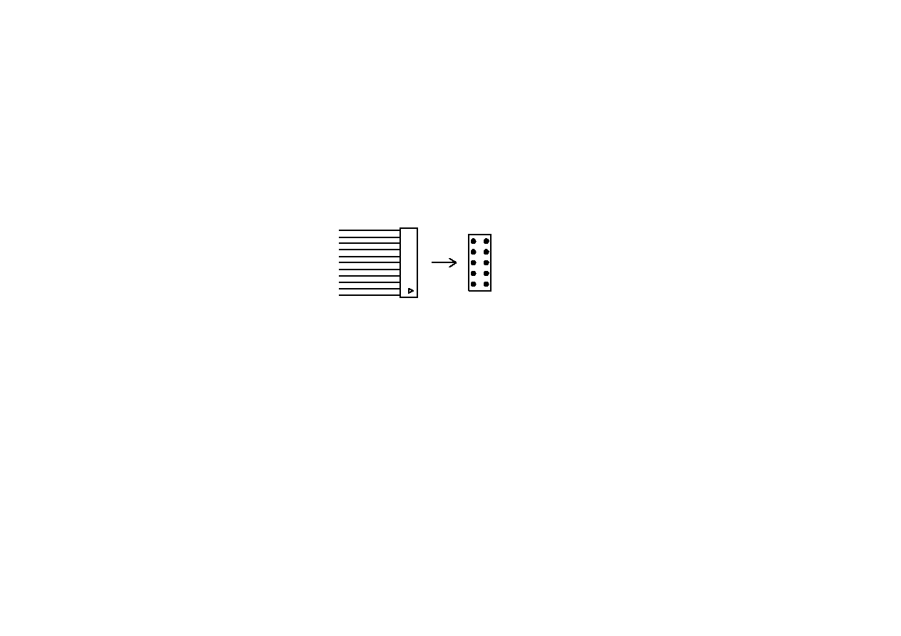
Indication of data
Input data is indicated on the register map. Red letter indicates "H" or "1" and blue one indicates "L" or "0". Blank is the
part that is not defined in the datasheet.
Attention on the operation
If you set up Function1 or Function2 dialog, input data to all boxes. Attention dialog is indicated if you input data or
address that is not specified in the datasheet or you click "OK" button before you input data. In that case set up the
dialog and input data once more again. These operations does not need if you click "Cancel" button or check the check
box.
ASAHI KASEI
[AKD4631-VN]
<KM077301>
2005/01
- 20 -
1.AK4631 Mode: EXT mode (Slave)
[Measurement condition]
∑ Measurement unit: ROHDE & SCHWARZ, UPD05
∑ MCKI: 256fs, 512fs
∑ BICK: 64fs
∑ Bit: 16bit
∑ Sampling Frequency: 8kHz & 16kHz
∑ Measurement Frequency: 20 3.4kHz (fs=8kHz), 20 8kHz (fs=16kHz)
∑ Power Supply: AVDD=DVDD=3.3V,SVDD=3.3V/5.0V
∑ Temperature: Room
∑ Input Frequency: 1kHz
[Measurement Results]
1.ADC characteristics (MIC Gain = +20dB, IPGA=0dB, ALC1 = OFF, MIC IPGA ADC)
Result
MCKI clock
512fs
256fs
Sampling Frequency
8kHz
16kHz
8kHz
16kHz
S/(N+D) (-1dBFS)
84.6dB
84.1dB
85.2dB
84.1dB
D-Range (-60dBFS)
86.1dB
85.0dB
88.6dB
84.9dB
S/N 86.1dB
85.0dB
88.6dB
85.0dB
2. DAC characteristics (AOUT) (DAC AOUT, DVOL = 0dB)
Result
MCKI clock
512fs
256fs
Sampling Frequency
8kHz
16kHz
8kHz
16kHz
S/(N+D) (0dBFS)
89.7dB
89.0dB
86.0dB
91.9dB
D-Range (-60dBFS)
93.5dB
91.1dB
93.7dB
95.3dB
S/N 94.1dB
92.2dB
94.5dB
95.3dB
3. Speaker-Amp characteristics (DAC MOUT MIN SPP/SPN, ALC2=OFF)
Result
SPKG1-0 = "00" (-0.5dBFS)
65.8dB
SVDD=3.3V
RL=8
SPKG1-0 = "01" (-0.5dBFS)
67.8dB
SPKG1-0 = "10" (-0.5dBFS)
74.5dB
S/(N+D)
SVDD=5.0V
RL=50
SPKG1-0 = "11" (-0.5dBFS)
78.1dB
SPKG1-0 = "00"
90.2dB
SVDD=3.3V
RL=8
SPKG1-0 = "01"
90.4dB
SPKG1-0 = "10"
90.3dB
S/N
SVDD=5.0V
RL=50
SPKG1-0 = "11"
90.4dB
4. Loop-back (MIC ADC DAC AOUT)
Result
MCKI clock
512fs
256fs
Sampling Frequency
8kHz
16kHz
8kHz
16kHz
S/(N+D) (-1dBFS)
84.4dB
84.0dB
84.7dB
84.0dB
D-Range (-60dBFS)
85.9dB
84.8dB
87.8dB
84.5dB
S/N 86.0dB
84.8dB
87.9dB
84.6dB
MEASUREMENT RESULTS EXAMPLE
ASAHI KASEI
[AKD4631-VN]
<KM077301>
2005/01
- 21 -
2.AK4631 Mode: PLL SLAVE mode
[Measurement condition]
∑ Measurement unit: ROHDE & SCHWARZ, UPD05
∑ Bit: 16bit
∑ Sampling Frequency: 8kHz & 16kHz
∑ Measurement Frequency: 20 3.4kHz (fs=8kHz), 20 8kHz (fs=16kHz)
∑ Power Supply: AVDD=DVDD=SVDD=3.3V
∑ Temperature: Room
∑ Input Frequency: 1kHz
[Measurement Results]
2-1. PLL Reference clock : BICK or FCK pin
Loop-back (MIC ADC DAC AOUT)
Result
PLL Reference clock
1fs (FCK pin)
16fs (BICK pin)
Sampling Frequency
8kHz
16kHz
8kHz
16kHz
S/(N+D) (-1dBFS)
65.1dB
72.2dB
85.0dB
83.6dB
D-Range (-60dBFS)
86.3dB
85.0dB
87.8dB
85.0dB
S/N 86.4dB
85.0dB
87.9dB
85.0dB
2-2. PLL Reference clock : MCKI pin
Loop-back (MIC ADC DAC AOUT)
Result
PLL Reference clock
12.288MHz
Sampling Frequency
8kHz
16kHz
S/(N+D) (-1dBFS)
84.5dB
83.4dB
D-Range (-60dBFS)
86.3dB
85.1dB
S/N 86.6dB
85.2dB
3.AK4631 Mode: PLL MASTER mode
[Measurement condition]
∑ Measurement unit: ROHDE & SCHWARZ, UPD05
∑ MCKI: 12.288 MHz
∑ BICK: 16fs
∑ Bit: 16bit
∑ Sampling Frequency: 8kHz & 16kHz
∑ Measurement Frequency: 20 3.4kHz (fs=8kHz), 20 8kHz (fs=16kHz)
∑ Power Supply: AVDD=DVDD=SVDD=3.3V
∑ Temperature: Room
∑ Input Frequency:1kHz
[Measurement Results]
Loop-back (MIC ADC DAC AOUT)
Result
8kHz 16kHz
S/(N+D) (-1dBFS)
84.4dB
83.9dB
D-Range (-60dBFS)
86.1dB
85.3dB
S/N 86.4dB
85.3dB
ASAHI KASEI
[AKD4631-VN]
<KM077301>
2005/01
- 22 -
4.PLOT DATA (EXT Slave mode)
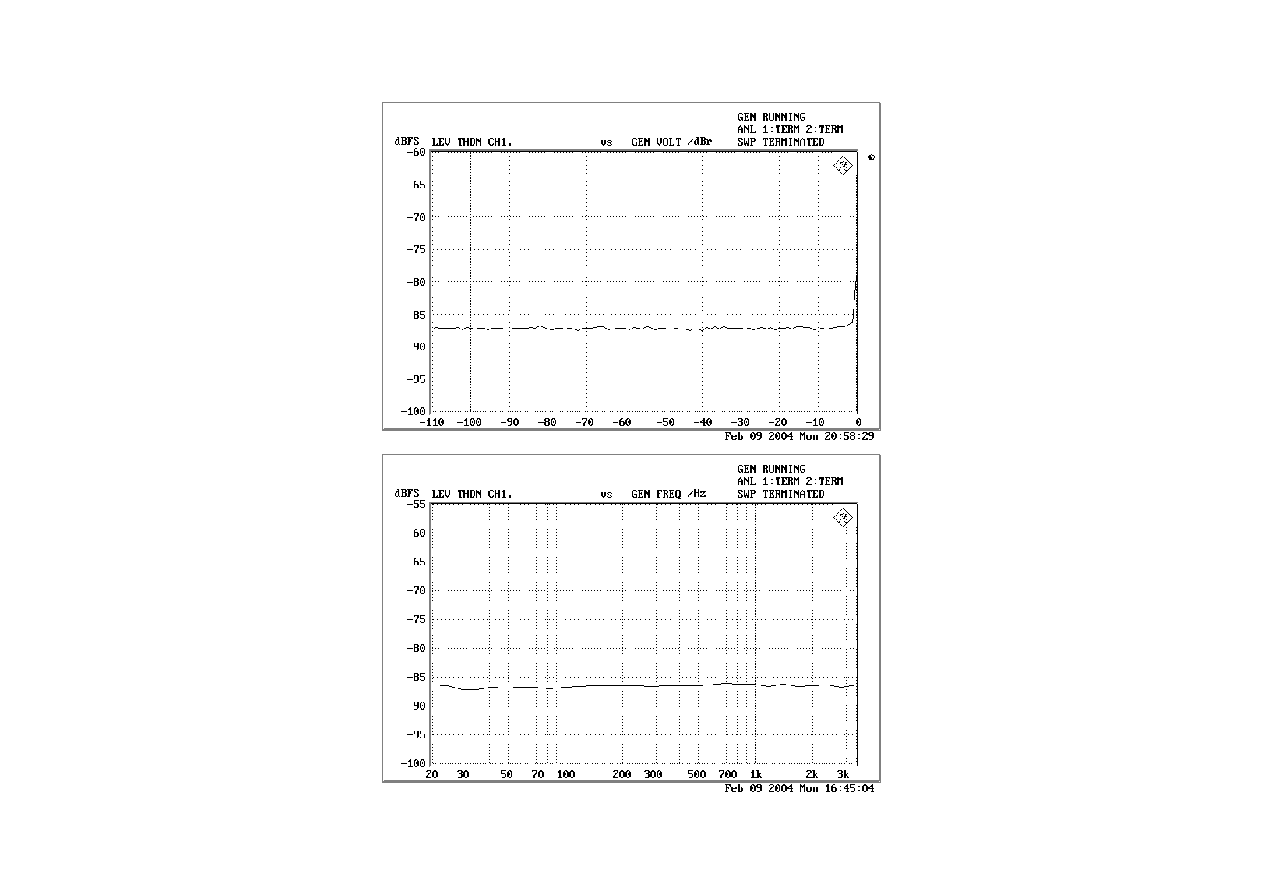
4-1.ADC (MIC ADC) PLOT DATA
Figure 8. THD+N vs. Input Level
Figure 9. THD+N vs. Input Frequency (Input Level = -1dBFS)
ASAHI KASEI
[AKD4631-VN]
<KM077301>
2005/01
- 23 -
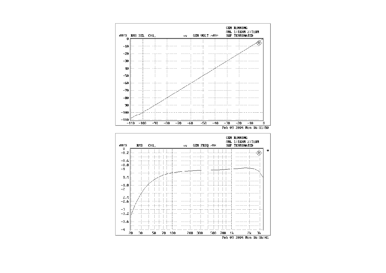
Figure 10. Linearity
Figure 11. Frequency Response
ASAHI KASEI
[AKD4631-VN]
<KM077301>
2005/01
- 24 -
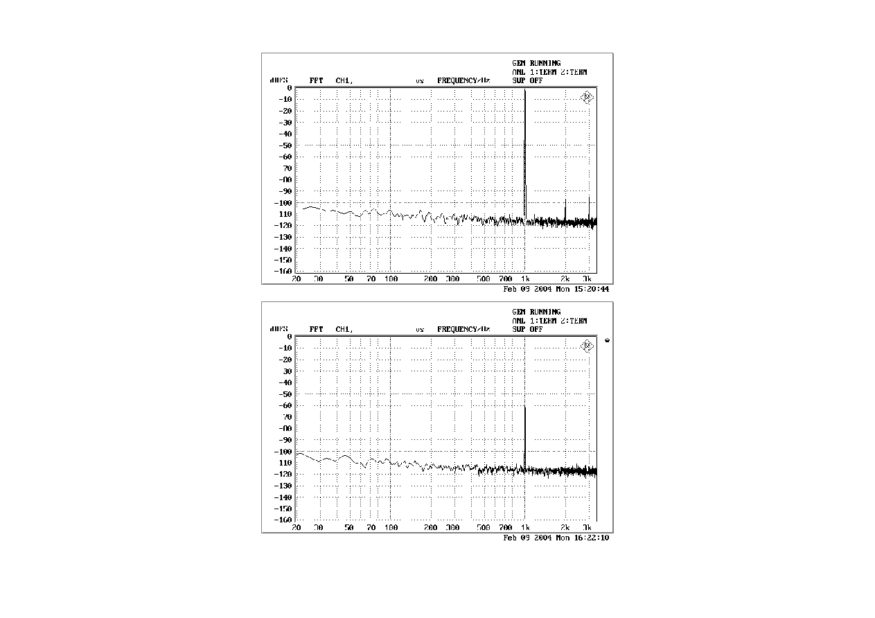
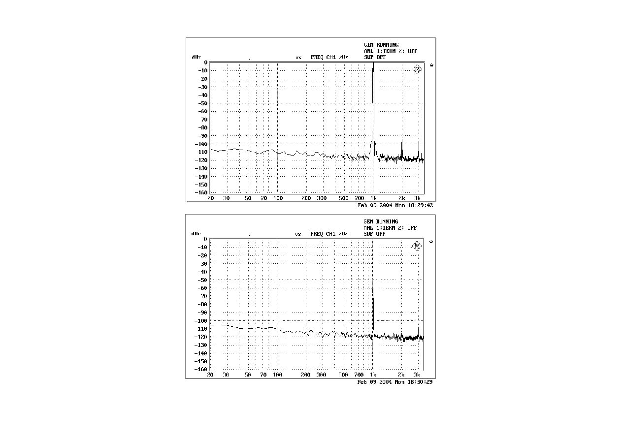
Figure 12. FFT Plot ( Input level=-1.0dBFS)
Figure 13. FFT Plot ( Input level=-60.0dBFS )
ASAHI KASEI
[AKD4631-VN]
<KM077301>
2005/01
- 25 -
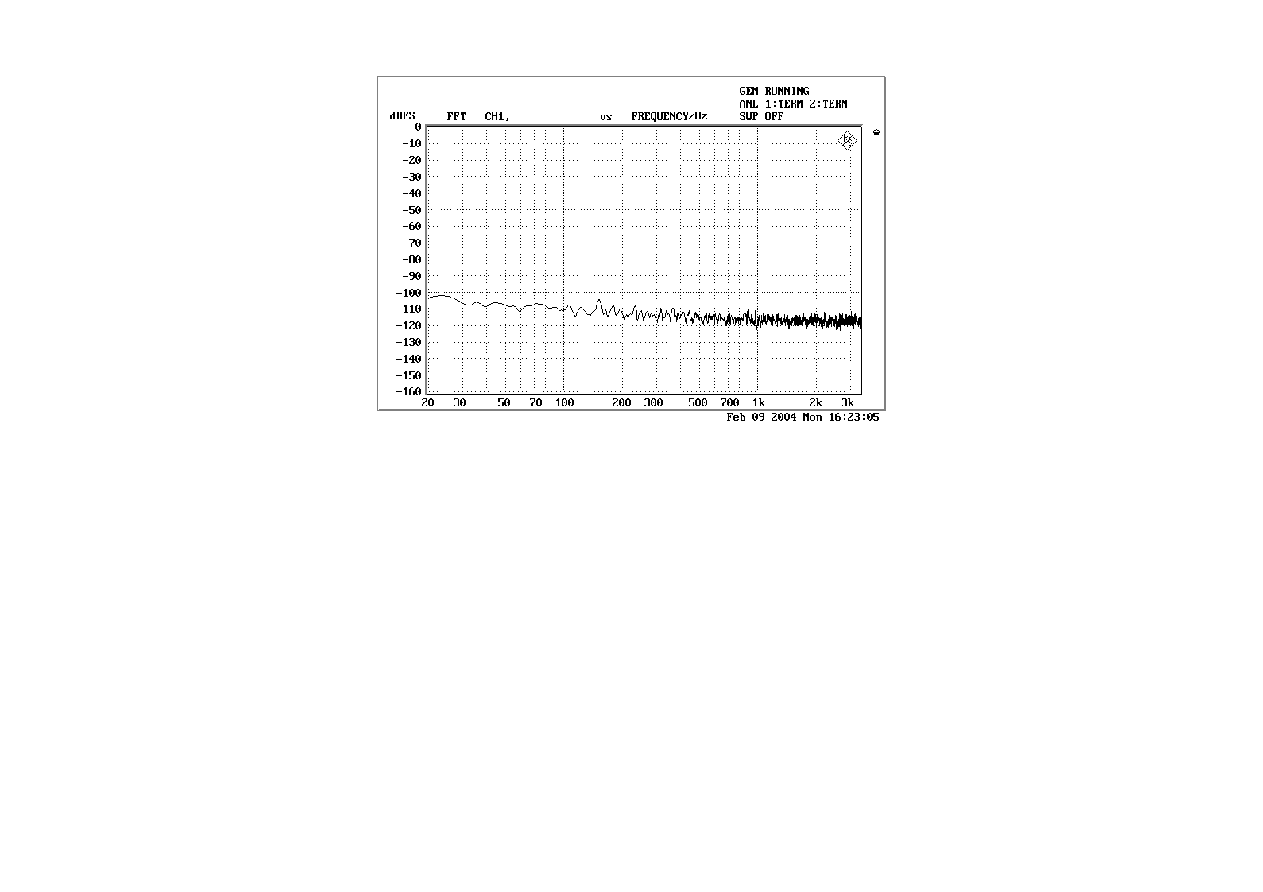
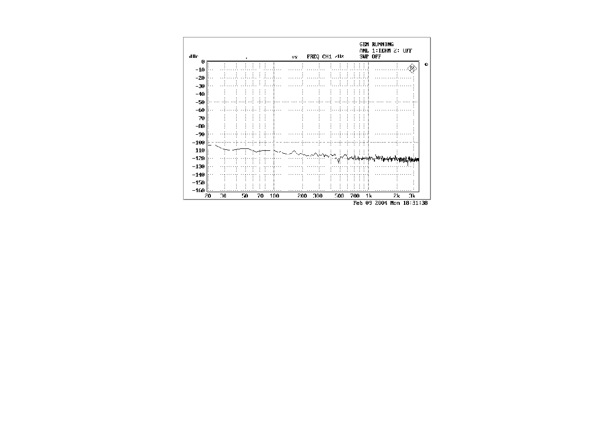
Figure 14. FFT Plot ( "0" data input )
ASAHI KASEI
[AKD4631-VN]
<KM077301>
2005/01
- 26 -
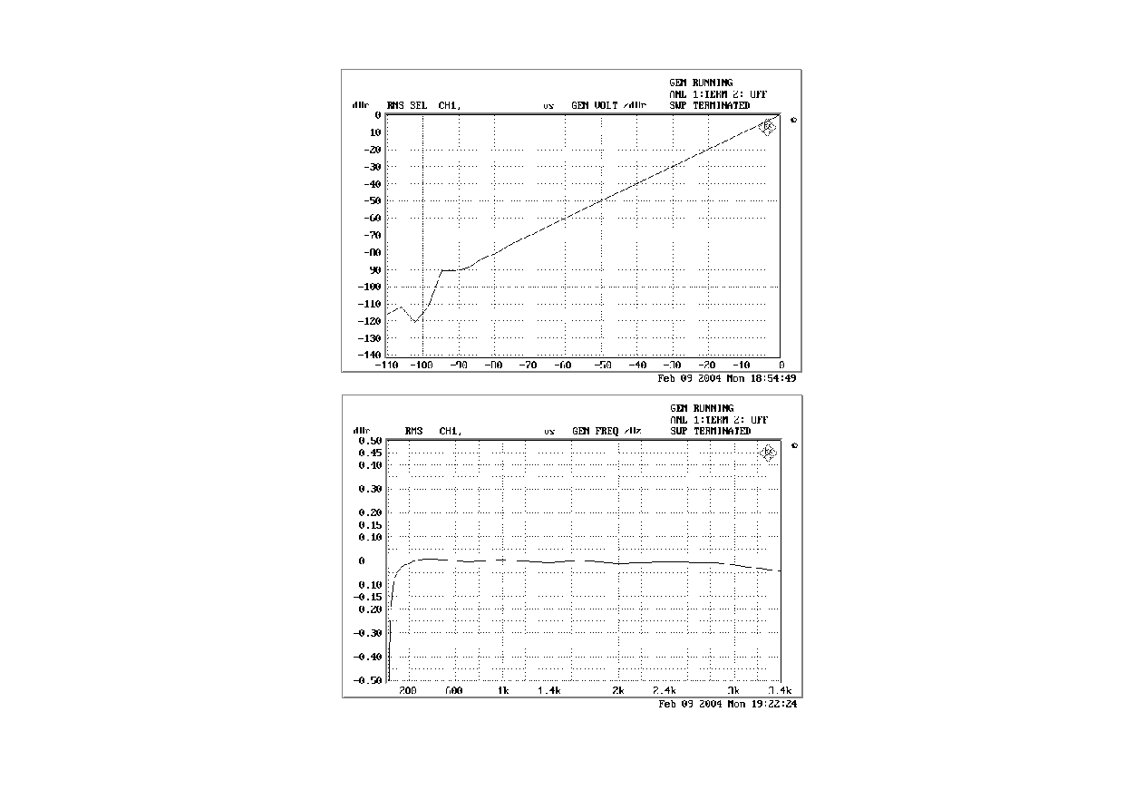
4-2. DAC (DAC AOUT) PLOT DATA
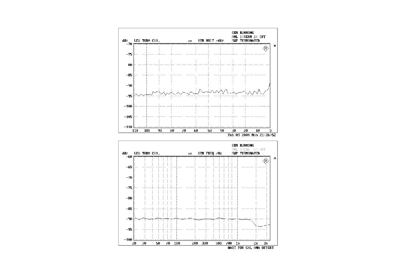
Figure 15. THD+N vs. Input Level
Figure 16. THD+N vs. Input Frequency (Input Level = 0dBFS)
ASAHI KASEI
[AKD4631-VN]
<KM077301>
2005/01
- 27 -
Figure 17. Linearity
Figure 18. Frequency Response
ASAHI KASEI
[AKD4631-VN]
<KM077301>
2005/01
- 28 -
Figure 19. FFT Plot ( Input level=0dBFS )
Figure 20. FFT Plot ( Input level=-60.0dBFS )
ASAHI KASEI
[AKD4631-VN]
<KM077301>
2005/01
- 29 -
Figure 21. FFT Plot ( "0" data input )
ASAHI KASEI
[AKD4631-VN]
<KM077301>
2005/01
- 30 -
Revision History
Date Manual
Revision
Board
Revision
Reason Contents
04/01/25 KM077300
0 First
Edition
IMPORTANT NOTICE
∑
These products and their specifications are subject to change without notice. Before considering
any use or application, consult the Asahi Kasei Microsystems Co., Ltd. (AKM) sales office or
authorized distributor concerning their current status.
∑
AKM assumes no liability for infringement of any patent, intellectual property, or other right in the
application or use of any information contained herein.
∑
Any export of these products, or devices or systems containing them, may require an export license
or other official approval under the law and regulations of the country of export pertaining to customs
and tariffs, currency exchange, or strategic materials.
∑
AKM products are neither intended nor authorized for use as critical components in any safety, life
support, or other hazard related device or system, and AKM assumes no responsibility relating to
any such use, except with the express written consent of the Representative Director of AKM. As
used here:
(a) A hazard related device or system is one designed or intended for life support or maintenance of
safety or for applications in medicine, aerospace, nuclear energy, or other fields, in which its
failure to function or perform may reasonably be expected to result in loss of life or in significant
injury or damage to person or property.
(b) A critical component is one whose failure to function or perform may reasonably be expected to
result, whether directly or indirectly, in the loss of the safety or effectiveness of the device or
system containing it, and which must therefore meet very high standards of performance and
reliability.
∑
It is the responsibility of the buyer or distributor of an AKM product who distributes, disposes of, or
otherwise places the product with a third party to notify that party in advance of the above content
and conditions, and the buyer or distributor agrees to assume any and all responsibility and liability
for and hold AKM harmless from any and all claims arising from the use of said product in the
absence of such notification.
A
A
B
B
C
C
D
D
E
E
E
E
D
D
C
C
B
B
A
A
SVDD
REG_IN
AVDD
DVDD
VCC(3.3V)
REG_IN
AVDD
DVDD
SVDD
4631_MCKI
INT
MOUT
4631_SDTO
SPN
BEEP
SPP
CCLK
4631_FCK
AOUT
MIN
AVDD
4631_BICK
DVDD
CDTI
REG
REG
REG
4631_MCKO
PDN
CSN
4631_SDTI
AVDD
DVDD
LVC
D3.3V
Title
Size
Document Number
Rev
Date:
Sheet
of
AK4631-VN
0
AKD4631-VN
A3
1
5
Wednesday, December 22, 2004
Title
Size
Document Number
Rev
Date:
Sheet
of
AK4631-VN
0
AKD4631-VN
A3
1
5
Wednesday, December 22, 2004
Title
Size
Document Number
Rev
Date:
Sheet
of
AK4631-VN
0
AKD4631-VN
A3
1
5
Wednesday, December 22, 2004
REG
SVDD
REG
AVDD
AVSS
SVSS
AVSS
AVSS
SVSS
DVDD
AVSS
AVDD
AVSS
AVSS
AVSS
SVSS
VCC
DVDD
LVC
VCC
AVSS
SVSS
AVSS
AVSS
AVSS
SVSS
1
TP22
SVDD
TP22
SVDD
C8
4.7n
C8
4.7n
JP6 MCKI
JP6 MCKI
C7
0.22u
C7
0.22u
IN
OUT
GND
T1
TA48033F
T1
TA48033F
1
TP29
MICOUT
TP29
MICOUT
+
C21
10u
+
C21
10u
+
C12
10u
+
C12
10u
1
TP3
AVSS
TP3
AVSS
1
TP13
SDTO
TP13
SDTO
1
TP23
SVSS
TP23
SVSS
R8
51
R8
51
R40
(short)
R40
(short)
1
2
+
C22
47u
+
C22
47u
1
2
L2
(short)
L2
(short)
1
TP18
MCKI
TP18
MCKI
JP9
DVDD_SEL
JP9
DVDD_SEL
25
26
27
28
29
30
31
32
CN1
32pin_4
CN1
32pin_4
1
TP25
MOUT
TP25
MOUT
R1410
R1410
JP1
GND
JP1
GND
R13
470
R13
470
1
TP14
FCK
TP14
FCK
1
TP2 AVDD
TP2 AVDD
C10
0.1u
C10
0.1u
R11
51
R11
51
R6
51
R6
51
JP2
AIN
JP2
AIN
1
TP9
CSN
TP9
CSN
1
SVSS
T45_BK
SVSS
T45_BK
1
TP24
MIN
TP24
MIN
C2
0.1u
C2
0.1u
JP4
SVDD_SEL
JP4
SVDD_SEL
9
10
11
12
13
14
15
16
CN4
32pin_2
CN4
32pin_2
R12
470
R12
470
C5
0.1u
C5
0.1u
R4
(open)
R4
(open)
1
TP19
MCKO
TP19
MCKO
1
TP1
VCOC
TP1
VCOC
1
TP26
AOUT
TP26
AOUT
+
C6
1u
+
C6
1u
1
TP10
CCLK
TP10
CCLK
1
TP15
BICK
TP15
BICK
1
2
+
C23
47u
+
C23
47u
1
REG
T45_R
REG
T45_R
1
SVDD
T45_BU
SVDD
T45_BU
JP10
LVC_SEL
JP10
LVC_SEL
R9
51
R9
51
1
TP30
MIC
TP30
MIC
1
TP21
SPP
TP21
SPP
1
2
3
4
5
6
7
8
CN2
32pin_1
CN2
32pin_1
R7
51
R7
51
1
2
L5
(short)
L5
(short)
R1
2.2k
R1
2.2k
1
TP8
PDN
TP8
PDN
C1
0.1u
C1
0.1u
1
2
L4
(short)
L4
(short)
+
C9
10u
+
C9
10u
1
TP16
DVDD
TP16
DVDD
1
TP27
BEEP
TP27
BEEP
1
TP11
CDTI
TP11
CDTI
1
AVSS
T45_BK
AVSS
T45_BK
C11
0.1u
C11
0.1u
1
DVDD
T45_O
DVDD
T45_O
1
TP31
MPI
TP31
MPI
17
18
19
20
21
22
23
24
CN3
32pin_3
CN3
32pin_3
1
2
+
C3
47u
+
C3
47u
VCOM
1
AVSS
2
AVDD
3
VCOC
4
PDN
5
CSN
6
CCLK
7
CDT
I
8
SD
TI
9
SD
TO
10
FC
K
11
BIC
K
12
DV
DD
13
D
VSS
14
MCKI
15
MCKO
16
SPP
17
SPN
18
SVDD
19
SVSS
20
MIN
21
MOU
T
22
AO
U
T
23
BEEP
24
AIN
25
M
I
COUT
26
MIC
27
MPI
28
U1
AK4631VN
U1
AK4631VN
1
2
+
C13
47u
+
C13
47u
1
2
L1
(short)
L1
(short)
R3 (short)
R3 (short)
1
2
+
C16
47u
+
C16
47u
+
C4
2.2u
+
C4
2.2u
1
TP28
AIN
TP28
AIN
1
TP20
SPN
TP20
SPN
R2
10k
R2
10k
1
TP12
SDTI
TP12
SDTI
JP3
AVDD_SEL
JP3
AVDD_SEL
JP11
VCC_SEL
JP11
VCC_SEL
1
DGND
T45_BK
DGND
T45_BK
1
TP32
VCOM
TP32
VCOM
1
AVDD
T45_O
AVDD
T45_O
C20
0.1u
C20
0.1u
R10
51
R10
51
R5 (short)
R5 (short)

A
A
B
B
C
C
D
D
E
E
E
E
D
D
C
C
B
B
A
A
MOUT
SPP
SPN
INT
AOUT
MIN
BEEP
Title
Size
Document Number
Rev
Date:
Sheet
of
Input/Output
0
AKD4631-VN
A3
2
5
Wednesday, December 22, 2004
Title
Size
Document Number
Rev
Date:
Sheet
of
Input/Output
0
AKD4631-VN
A3
2
5
Wednesday, December 22, 2004
Title
Size
Document Number
Rev
Date:
Sheet
of
Input/Output
0
AKD4631-VN
A3
2
5
Wednesday, December 22, 2004
IN
OUT
JACK
AVSS
AVSS
AVSS
AVSS
AVSS
AVSS
2
3
MIC
1
RCA
BEEP/MIN/MOUT
2
3
1
AVSS
MOUT
MIN
BEEP
L
R
020S16
SPK1
SVSS
Dynamic(EXT)
Dynamic
Piezo(EXT)
SVSS
Dynamic(EXT)
Piezo(EXT)
Dynamic
3
1
2
AOUT
SVSS
JP15
MIN/MOUT
JP15
MIN/MOUT
JP12
MIC_SEL
JP12
MIC_SEL
R18
47k
R18
47k
R21
20k
R21
20k
J3
MR-552LS
J3
MR-552LS
1
2
+
C26
1u
+
C26
1u
J4
MR-552LS
J4
MR-552LS
R15
10
R15
10
JP16
BEEP/MIN/MOUT
JP16
BEEP/MIN/MOUT
A
K
D1
DIODE ZENER
D1
DIODE ZENER
R20
220
R20
220
C25
0.1u
C25
0.1u
JP13
SPN_SEL
JP13
SPN_SEL
R17
10
R17
10
6
4
3
J2
SPK-JACK
J2
SPK-JACK
R19
20k
R19
20k
JP31
Dynamic
JP31
Dynamic
1
2
+
C24
1u
+
C24
1u
J5
MR-552LS
J5
MR-552LS
JP14
SPP_SEL
JP14
SPP_SEL
6
4
3
J1
MIC-JACK
J1
MIC-JACK
R16
20k
R16
20k
A
K
D2
DIODE ZENER
D2
DIODE ZENER
1
2
CN5
CN5
1
2
+
C28
1u
+
C28
1u
A
A
B
B
C
C
D
D
E
E
E
E
D
D
C
C
B
B
A
A
VCC
VCC
EXT_MCLK
EXT_BICK
MCKO
DIR_MCLK
EXT_FCK
D3.3V
Title
Size
Document Number
Rev
Date:
Sheet
of
CLOCK
0
AKD4631-VN
A3
3
5
Wednesday, December 22, 2004
Title
Size
Document Number
Rev
Date:
Sheet
of
CLOCK
0
AKD4631-VN
A3
3
5
Wednesday, December 22, 2004
Title
Size
Document Number
Rev
Date:
Sheet
of
CLOCK
0
AKD4631-VN
A3
3
5
Wednesday, December 22, 2004
EXT
1024fs
64fs
512fs
256fs
32fs
INV
THR
16fs
1fs
XTL
EXT
EXT
for
74HCU04,74AC74,74VHC4040,74HC14,74HC14,74HC541,74HCT04
MCKO
DIR
3
1
EXT/BICK
AVSS
2
2
FCK
1
3
AVSS
2fs
D
2
CLK
3
Q
5
Q
6
PR
4
CL
1
U4A
74AC74
U4A
74AC74
JP18
MKFS
JP18
MKFS
C33
0.1u
C33
0.1u
R26
51
R26
51
R27
51
R27
51
C34
0.1u
C34
0.1u
JP22
FCK_SEL
JP22
FCK_SEL
J8
MR-552LS
J8
MR-552LS
R25
short
R25
short
1
2
U5A
74HC14
U5A
74HC14
R24
1M
R24
1M
1
2
U2A
74HCU04
U2A
74HCU04
1
2
X1
12.288MHz
X1
12.288MHz
3
4
U2B
74HCU04
U2B
74HCU04
D
12
CLK
11
Q
9
Q
8
PR
10
CL
13
U4B
74AC74
U4B
74AC74
C36
0.1u
C36
0.1u
JP17
XTE
JP17
XTE
C35
0.1u
C35
0.1u
C31
0.1u
C31
0.1u
J9
MR-552LS
J9
MR-552LS
1
2
+
C37
47u
+
C37
47u
JP23
EXT1
JP23
EXT1
C39
5p
C39
5p
CLK
10
RST
11
Q1
9
Q2
7
Q3
6
Q4
5
Q5
3
Q6
2
Q7
4
Q8
13
Q9
12
Q10
14
Q11
15
Q12
1
U3
74VHC4040
U3
74VHC4040
C30
0.1u
C30
0.1u
C38
5p
C38
5p
JP20
BICK
JP20
BICK
C32
0.1u
C32
0.1u
JP24
EXT2
JP24
EXT2
JP19
BICK_SEL
JP19
BICK_SEL
JP21
MCLK_SEL
JP21
MCLK_SEL
A
A
B
B
C
C
D
D
E
E
E
E
D
D
C
C
B
B
A
A
DAUX
DIR_SDTI
DIR_BICK
DIR_FCK
CM0
CM0
D3.3V
D3.3V
CM1
OCKS0
CM1
OCKS1
D3.3V
D3.3V
M/S
D3.3V
D3.3V
D3.3V
OCKS1
OCKS0
DIR_MCLK
Title
Size
Document Number
Rev
Date:
Sheet
of
DIR/DIT
0
AKD4631-VN
A3
4
5
Wednesday, December 22, 2004
Title
Size
Document Number
Rev
Date:
Sheet
of
DIR/DIT
0
AKD4631-VN
A3
4
5
Wednesday, December 22, 2004
Title
Size
Document Number
Rev
Date:
Sheet
of
DIR/DIT
0
AKD4631-VN
A3
4
5
Wednesday, December 22, 2004
H
L
DIF0
DIF2
CM0
OCKS1
M/S
CM1
DIF1
OCKS0
MCKO2
MCKO1
1
2
+
C43
10u
+
C43
10u
C41
0.1u
C41
0.1u
C46
0.47u
C46
0.47u
IPS0
1
NC
2
DIF0
3
TEST2
4
DIF1
5
NC
6
DIF2
7
IPS1
8
P/SN
9
XTL0
10
XTL1
11
TVD
D
13
D
VSS
14
TX0
15
TX1
16
BO
U
T
17
COUT
18
UOUT
19
VO
U
T
20
DV
DD
21
D
VSS
22
MC
KO1
23
BICK
26
MCKO2
27
DAUX
28
XTO
29
XTI
30
PDN
31
CM0
32
CM1
33
OCKS1
34
OCKS0
35
INT0
36
AVD
D
38
R
39
VC
O
M
40
AVSS
41
RX
0
42
NC
43
RX
1
44
TEST1
45
RX
2
46
NC
47
RX
3
48
VIN
12
LRCK
24
SDTO
25
IN
T1
37
U6
AK4114
U6
AK4114
C44
0.1u
C44
0.1u
1
2
+
C51
10u
+
C51
10u
5
6
U5C
74HC14
U5C
74HC14
K
A
D3
HSU119
D3
HSU119
C49
0.1u
C49
0.1u
C53
0.1u
C53
0.1u
C48
5p
C48
5p
1
2
+
C52
10u
+
C52
10u
1
2
U7A
74HC04
U7A
74HC04
C50
0.1u
C50
0.1u
C47
5p
C47
5p
C45
0.1u
C45
0.1u
1
2
3
4
5
6
7
8
16
15
14
13
12
11
10
9
SW3
SW3
R31
1k
R31
1k
3
4
U5B
74HC14
U5B
74HC14
R29
470
R29
470
1
2
X2
11.2896MHz
X2
11.2896MHz
C42
0.1u
C42
0.1u
K
A
LED1
ERF
LED1
ERF
R30
18k
R30
18k
R28
10k
R28
10k
JP25
MCKO_SEL
JP25
MCKO_SEL
C40
0.1u
C40
0.1u
2
1
3
SW1
DIR
SW1
DIR
GND
1
VCC
2
IN
3
PORT2
TOTX141
PORT2
TOTX141
OUT
1
VCC
3
GND
2
PORT1
TORX141
PORT1
TORX141
1
2
L6
(short)
L6
(short)
1
2
3
4
5
6
7
8
9
RP1
47k
RP1
47k
A
A
B
B
C
C
D
D
E
E
E
E
D
D
C
C
B
B
A
A
4631_SDTI
4631_MCKI
DAUX
4631_FCK
4631_BICK
LVC
DAUX
EXT_BICK
DIR_SDTI
4631_MCKI
DIR_FCK
EXT_FCK
4631_MCKO
M/S
MCKO
4631_SDTO
EXT_MCLK
DIR_BICK
D3V
LVC
D3V
D3V
CSN
CCLK
CDTI
PDN
Title
Size
Document Number
Rev
Date:
Sheet
of
LOGIC
0
AKD4631-VN
A3
5
5
Wednesday, December 22, 2004
Title
Size
Document Number
Rev
Date:
Sheet
of
LOGIC
0
AKD4631-VN
A3
5
5
Wednesday, December 22, 2004
Title
Size
Document Number
Rev
Date:
Sheet
of
LOGIC
0
AKD4631-VN
A3
5
5
Wednesday, December 22, 2004
FCK
ADC
ADC
DIR
MCLK
VCC
SDTI
DIR
BICK
CCLK
CDTI
CSN
L
H
ADC
DIR
INV
THR
DAC/LOOP
ADC
JP27
BICK
JP27
BICK
JP26
4631_SDTI
JP26
4631_SDTI
6
5
4
3
2
1
7
RP3
47k
RP3
47k
C57
0.1u
C57
0.1u
1
2
3
4
5
6
7
8
9
10
PORT4
CTRL
PORT4
CTRL
13
12
U10F
74HC14
U10F
74HC14
C55
0.1u
C55
0.1u
R38
10k
R38
10k
A1
2
Y1
18
A2
3
Y2
17
A3
4
Y3
16
A4
5
Y4
15
A5
6
Y5
14
A6
7
Y6
13
A7
8
Y7
12
A8
9
Y8
11
G1
1
G2
19
U11
74HC541
U11
74HC541
R37
470
R37
470
11
10
U10E
74HC14
U10E
74HC14
1
2
3
4
5
6
7
8
9
10
PORT3
ROM
PORT3
ROM
2
1
3
SW2
PDN
SW2
PDN
9
8
U5D
74HC14
U5D
74HC14
9
8
U10D
74HC14
U10D
74HC14
R32
10k
R32
10k
R35
470
R35
470
6
5
4
3
2
1
7
RP2
47k
RP2
47k
13
12
U2F
74HCU04
U2F
74HCU04
13
12
U7F
74HC04
U7F
74HC04
R34
10k
R34
10k
5
6
U10C
74HC14
U10C
74HC14
11
10
U2E
74HCU04
U2E
74HCU04
A1
2
A2
3
A3
4
A4
5
A5
6
A6
7
A7
8
A8
9
G1
1
G2
19
Y1
18
Y2
17
Y3
16
Y4
15
Y5
14
Y6
13
Y7
12
Y8
11
VCC
20
GND
10
U9
74LVC541
U9
74LVC541
1
2
U10A
74HC14
U10A
74HC14
R39
10k
R39
10k
R36
10k
R36
10k
JP28
FCK
JP28
FCK
C54
0.1u
C54
0.1u
11
10
U7E
74HC04
U7E
74HC04
K
A
D4
HSU119
D4
HSU119
JP29
BICK_INV
JP29
BICK_INV
R33
470
R33
470
9
8
U2D
74HCU04
U2D
74HCU04
1
2
+
C56
47u
+
C56
47u
5
6
U2C
74HCU04
U2C
74HCU04
9
8
U7D
74HC04
U7D
74HC04
11
10
U5E
74HC14
U5E
74HC14
A1
2
A2
3
A4
5
A5
6
A6
7
A7
8
A8
9
DIR
1
G
19
B1
18
B2
17
B3
16
B4
15
B5
14
B6
13
B7
12
B8
11
VCC
20
GND
10
A3
4
U8
74LVC245
U8
74LVC245
3
4
U10B
74HC14
U10B
74HC14
5
6
U7C
74HC04
U7C
74HC04
JP30
SDTI
JP30
SDTI
3
4
U7B
74HC04
U7B
74HC04
AKD4631-VNL1 SILK
AKD4631-VNL2 SILK
AKD4631-VN L1
AKD4631-VNL2