GENERAL DESCRIPTION
The ALD1102 is a monolithic dual P-channel matched transistor pair
intended for a broad range of analog applications. These enhancement-
mode transistors are manufactured with Advanced Linear Devices' en-
hanced ACMOS silicon gate CMOS process.
The ALD1102 offers high input impedance and negative current tempera-
ture coefficient. The transistor pair is matched for minimum offset voltage
and differential thermal response, and it is designed for switching and
amplifying applications in +2V to +12V systems where low input bias
current, low input capacitance and fast switching speed are desired. Since
these are MOSFET devices, they feature very large (almost infinite) current
gain in a low frequency, or near DC operating environment. When used
with an ALD1101, a dual CMOS analog switch can be constructed. In
addition, the ALD1102 is intended as a building block for differential
amplifier input stages, transmission gates, and multiplexer applications.
The ALD1102 is suitable for use in precision applications which require
very high current gain, beta, such as current mirrors and current sources.
The high input impedance and the high DC current gain of the Field Effect
Transistors result in extremely low current loss through the control gate.
The DC current gain is limited by the gate input leakage current, which is
specified at 50pA at room temperature. For example, DC beta of the device
at a drain current of 5mA at 25
∞
C is = 5mA/50pA = 100,000,000.
FEATURES
∑ Low threshold voltage of 0.7V
∑ Low input capacitance
∑ Low Vos grades -- 2mV, 5mV, 10mV
∑ High input impedance -- 10
12
typical
∑ Low input and output leakage currents
∑ Negative current (I
DS
) temperature coefficient
∑ Enhancement-mode (normally off)
∑ DC current gain 10
9
APPLICATIONS
∑ Precision current mirrors
∑ Precision current sources
∑ Analog switches
∑ Choppers
∑ Differential amplifier
input stage
∑ Voltage comparator
∑ Data converters
∑ Sample and Hold
∑ Analog inverter
A
DVANCED
L
INEAR
D
EVICES,
I
NC.
DUAL P-CHANNEL MATCHED MOSFET PAIR
ALD1102A/ALD1102B
ALD1102
Operating Temperature Range*
-55
∞
C to +125
∞
C
0
∞
C to +70
∞
C
0
∞
C to +70
∞
C
8-Pin
8-Pin
8-Pin
CERDIP
Plastic Dip
SOIC
Package
Package
Package
ALD1102A PA
ALD1102B PA
ALD1102 DA
ALD1102 PA
ALD1102 SA
* Contact factory for industrial temperature range.
ORDERING INFORMATION
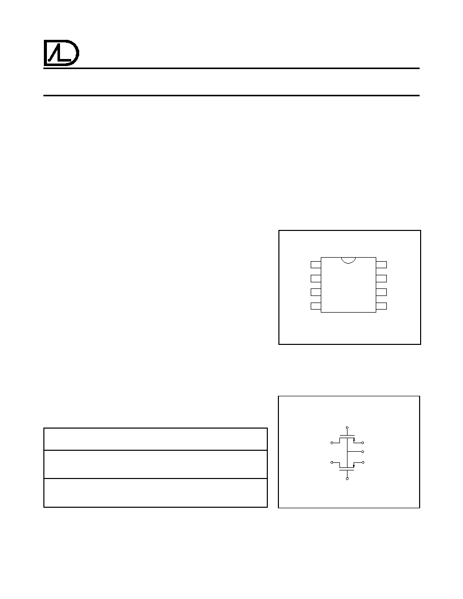
PIN CONFIGURATION
1
2
3
4
8
7
6
5
SOURCE
1
GATE
1
DRAIN
1
NC
SUBSTRATE
SOURCE
2
GATE
2
DRAIN
2
TOP VIEW
DA, PA, SA PACKAGE
SOURCE 1 (1)
SUBSTRATE (8)
SOURCE 2 (7)
GATE 2 (6)
DRAIN 1 (3)
GATE 1 (2)
DRAIN 2 (5)
BLOCK DIAGRAM
© 1998 Advanced Linear Devices, Inc. 415 Tasman Drive, Sunnyvale, California 94089 -1706 Tel: (408) 747-1155 Fax: (408) 747-1286 http://www.aldinc.com
© 1998 Advanced Linear Devices, Inc. 415 Tasman Drive, Sunnyvale, California 94089 -1706 Tel: (408) 747-1155 Fax: (408) 747-1286 http://www.aldinc.com
ALD1102A/ALD1102B
Advanced Linear Devices
2
ALD1102
ABSOLUTE MAXIMUM RATINGS
Drain-source voltage, V
DS
-13.2V
Gate-source voltage, V
GS
-13.2V
Power dissipation
500 mW
Operating temperature range
PA, SA package
0
∞
C to +70
∞
C
DA package
-55
∞
C to +125
∞
C
Storage temperature range
-65
∞
C to +150
∞
C
Lead temperature, 10 seconds
+260
∞
C
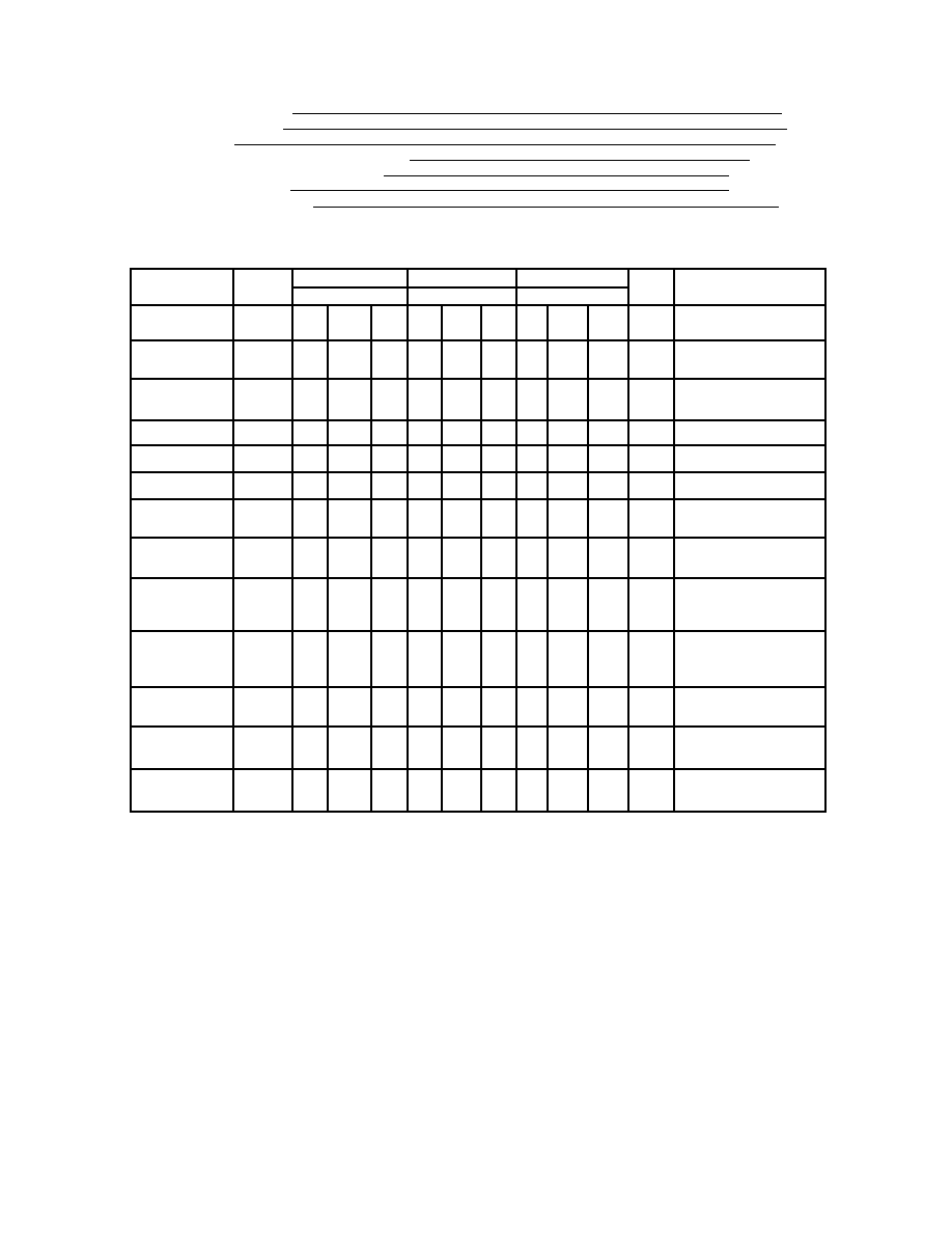
Gate Threshold
Voltage
V
T
-0.4
-0.7
-1.2
-0.4
-0.7
-1.2
-0.4
-0.7
-1.2
V
I
DS
= -10
µ
A V
GS
= V
DS
Offset Voltage
V
OS
2
5
10
mV
I
DS
= -100
µ
A V
GS
= V
DS
V
GS1
- V
GS2
Gate Threshold
TC
VT
-1.3
-1.3
-1.3
mV/
∞
C
Temperature Drift
On Drain Current
I
DS (ON)
-8
-16
-8
-16
-8
-16
mA
V
GS
= V
DS
= -5V
Transconductance G
fs
2
4
2
4
2
4
mmho
V
DS
= -5V I
DS
= -10mA
Mismatch
G
fs
0.5
0.5
0.5
%
Output
G
OS
500
500
500
µ
mho
V
DS
= -5V I
DS
= -10mA
Conductance
Drain Source
R
DS(ON)
180
270
180
270
180
270
V
DS
= -0.1V V
GS
= -5V
ON Resistance
Drain Source
ON Resistance
R
DS(ON)
0.5
0.5
0.5
%
V
DS
= -0.1V V
GS
= -5V
Mismatch
Drain Source
Breakdown
BV
DSS
-12
-12
-12
V
I
DS
= -10
µ
A V
GS
=0V
Voltage
Off Drain Current
I
DS(OFF)
0.1
4
0.1
4
0.1
4
nA
V
DS
=-12V V
GS
= 0V
4
4
4
µ
A
T
A
= 125
∞
C
Gate Leakage
I
GSS
1
50
1
50
1
50
pA
V
DS
=0V V
GS
=-12V
Current
10
10
10
nA
T
A
= 125
∞
C
Input
C
ISS
6
10
6
10
6
10
pF
Capacitance
OPERATING ELECTRICAL CHARACTERISTICS
T
A
= 25
∞
C unless otherwise specified
1102A 1102B 1102
Test
Parameter
Symbol
Min
Typ
Max
Min
Typ
Max
Min
Typ
Max
Unit
Conditions
ALD1102A/ALD1102B
Advanced Linear Devices
3
ALD1102
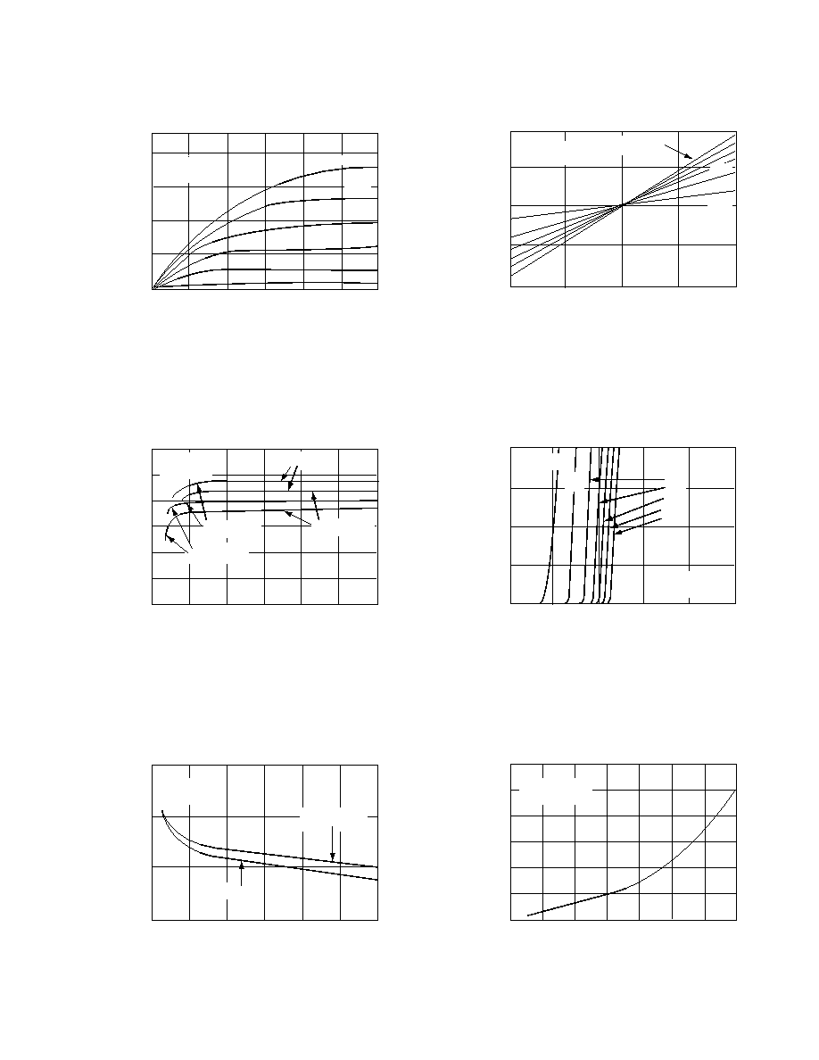
TYPICAL PERFORMANCE CHARACTERISITCS
OUTPUT CHARACTERISTICS
DRAIN - SOURCE VOLTAGE (V)
DRAIN - SOURCE CURRENT
(mA)
-80
-60
-40
-20
0
V
BS
= 0V
T
A
= 25
∞
C
-10V
-8V
-6V
-4V
-2V
0
-8
-2
-6
-4
-10
-12
V
GS
= -12V
LOW VOLTAGE OUTPUT
CHARACTERISTICS
DRAIN -SOURCE VOLTAGE (mV)
DRAIN-SOURCE CURRENT
(mA)
-320
-160
0
160
320
-4
4
2
0
-2
-4V
V
GS
= -12V
-6V
V
BS
= 0V
T
A
= 25
∞
C
-2V
-12
FORWARD TRANSCONDUCTANCE
vs. DRAIN - SOURCE VOLTAGE
DRAIN - SOURCE VOLTAGE (V)
0
-8
-2
-6
-4
-10
FORWARD TRANSCONDUCTANCE
(
µ
mho)
10000
5000
2000
1000
500
200
100
V
BS
= 0V
f = 1KHz
I
DS
= -5mA
T
A
= +125
∞
C
T
A
= +25
∞
C
I
DS
= -1mA
TRANSFER CHARACTERISTIC
WITH SUBSTRATE BIAS
GATE - SOURCE VOLTAGE (V)
0
-0.8
-1.6
-2.4
-3.2
-4.0
-20
-15
-10
-5
0
DRAIN-SOURCE CURRENT
(
µ
A)
V
BS
= 0V
4V
6V
8V
10V
12V
V
GS
= V
DS
T
A
= 25
∞
C
2V
GATE - SOURCE VOLTAGE (V)
R
DS (ON)
vs. GATE - SOURCE VOLTAGE
DRAIN - SOURCE ON RESISTANCE
(
)
10000
1000
100
10
-2
0
-4
-6
-8
-10
-12
V
DS
= 0.4V
V
BS
= 0V
T
A
= +125
∞
C
T
A
= +25
∞
C
OFF DRAIN - CURRENT vs.
TEMPERATURE
TEMPERATURE (
∞
C)
OFF - DRAIN SOURCE CURRENT
(A)
-50
-25
+25
+50
+75
+125
+100
0
-10
X
10
-6
V
DS
= -12V
V
GS
= V
BS
= 0V
-10
X
10
-12
-10
X
10
-9
