Operating Temperature Range *
-55
∞
C to +125
∞
C
0
∞
C to +70
∞
C
0
∞
C to +70
∞
C
8-Pin
Q8-Pin
8-Pin
CERDIP
Small Outline
Plastic Dip
Package
Package (SOIC)
Package
ALD2303A DA
ALD2303A SA
ALD2303A PA
ALD2303 DA
ALD2303 SA
ALD2303 PA
DUAL PRECISION MICROPOWER CMOS VOLTAGE COMPARATOR WITH DRIVER
ALD2303A/ALD2303
ORDERING INFORMATION
APPLICATIONS
∑ Sensor detection circuits
∑ PCMCIA instruments
∑ MOSFET driver
∑ High source impedance voltage
comparison circuits
∑ Multiple limit window comparator
∑ Power supply voltage monitor
∑ Photodetector sensor circuit
∑ High speed LED driver
∑ Oscillators
∑ Battery operated instruments
∑ Remote signal detection
∑ Multiple relay drivers
BENEFITS
∑ Extremely low power and high precision combination
∑ Built-in high input impedance buffer
∑ Built-in output driver with up to 60mA sink current
A
DVANCED
L
INEAR
D
EVICES,
I
NC.
FEATURES
∑ 3V, 5V and 12V supply
∑ Guaranteed to drive 200
loads
∑ Fanout of 30LS TTL loads
∑ Guaranteed maximum supply current of
20
µ
A for each comparator
∑ Pinout of LM193 type industry standard
comparators
∑ Extremely low input bias currents -- 10pA
∑ Virtually eliminates source impedance
effects
∑ Single (+5V) and dual supply (
±
5V)
operation
∑ CMOS, NMOS and TTL compatible
∑ Open drain wired-OR outputs
∑ High output sinking current -- 60mA
∑ Low supply current spikes
∑ High gain -- 100V/mV
GENERAL DESCRIPTION
The ALD2303A/ALD2303 is a precision monolithic high performance
dual voltage comparator built with advanced silicon gate CMOS tech-
nology. It features very high typical input impedance of 10
12
; low
input bias current of 10pA; very low power dissipation of 7.5
µ
A per
comparator; and single (+5V) or dual (
±
5V) power supply operation.
The input voltage range includes ground, making this comparator ideal
for single supply low level signal detection with high source impedance.
The ALD2303A/ALD2303 can be used in connection with other voltage
comparator circuits such as the ALD2301/ALD2302/ALD4302 voltage
comparators. The output can be connected to a higher external voltage
than V
+.
The ALD2303A/ALD2303 is ideal for high precision micropower voltage
comparator applications, especially low level signal detection circuits
requiring low standby power, yet retaining high output current
capability.
* Contact factory for industrial temperature range
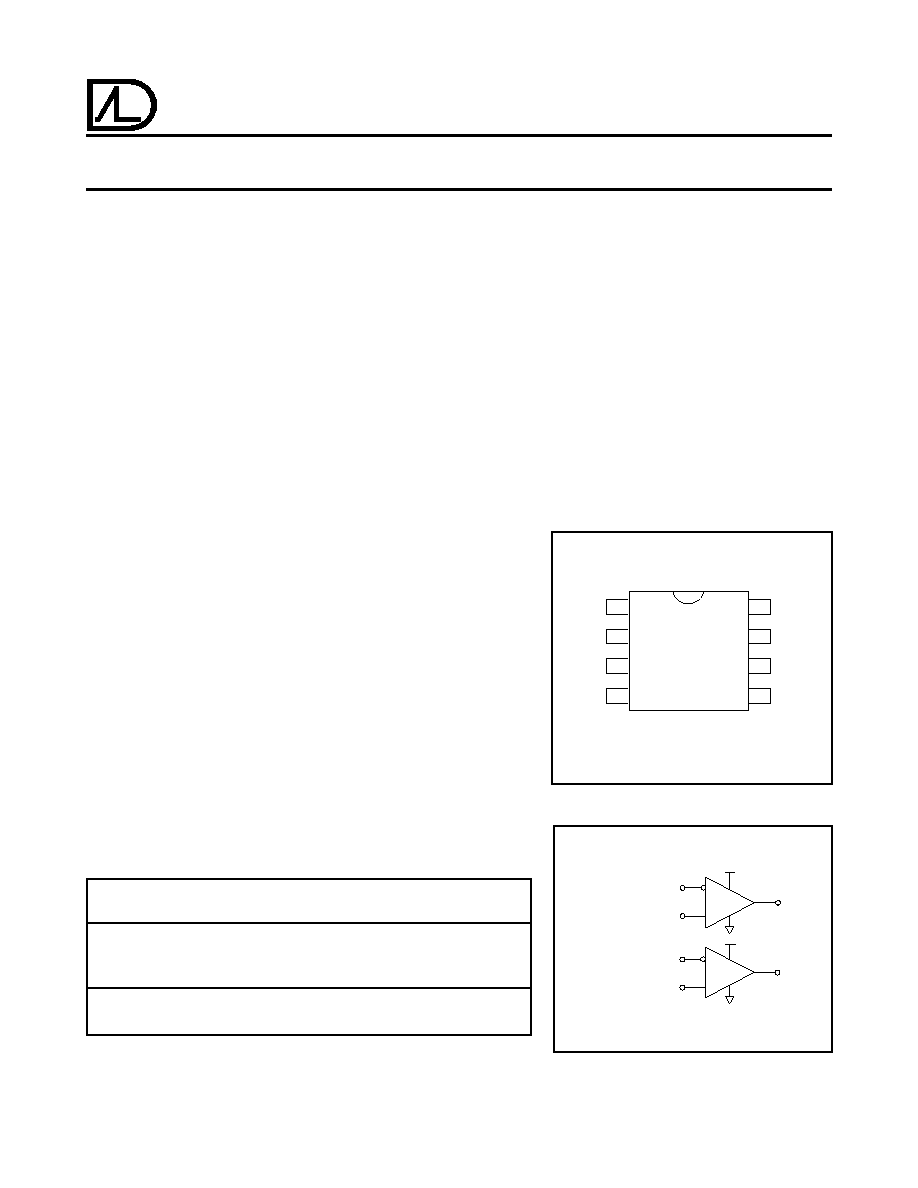
PIN CONFIGURATION
BLOCK DIAGRAM
1
2
3
4
8
7
6
5
OUT 1
-IN 1
+IN 1
GND
V+
OUT 2
-IN 2
+IN 2
TOP VIEW
DA, PA, SA PACKAGE
(1) OUT
1
(7) OUT
2
(4) GND
V
+
NONINVERTING INPUT
+IN
1
(3)
INVERTING INPUT
-IN
2
(6)
NONINVERTING INPUT
+IN
2
(5)
INVERTING INPUT
-IN
1
(2)
(8) V
+
© 1998 Advanced Linear Devices, Inc. 415 Tasman Drive, Sunnyvale, California 94089 -1706 Tel: (408) 747-1155 Fax: (408) 747-1286 http://www.aldinc.com

ALD2303A/ALD2303
Advanced Linear Devices
14
ABSOLUTE MAXIMUM RATINGS
Supply voltage, V
+
13.2V
Differential input voltage range
-0.3V to V
+
+0.3V
Power dissipation
600 mW
Operating temperature range
PA, SA package
0
∞
C to +70
∞
C
DA package
-55
∞
C to +125
∞
C
Storage temperature range
-65
∞
C to +150
∞
C
Lead temperature, 10 seconds
+260
∞
C
OPERATING ELECTRICAL CHARACTERISTICS
T
A
= 25
∞
C V+= +5V unless otherwise specified
2303A
2303
Test
Parameter
Symbol
Min
Typ
Max
Min
Typ
Max
Unit
Conditions
Notes:
1
Consists of junction leakage currents
2
Sample tested parameters
Voltage
V
S
±
1.5
±
6
±
1.5
±
6
V
Dual Supply
Supply
V
+
3
12
3
12
V
Single Supply
Supply
I
S
15
40
15
40
µ
A
R
LOAD
=
Current
Voltage
A
VD
10
100
10
100
V/mV
R
LOAD
15K
Gain
Input Offset
V
OS
0.5
1.0
1.5
4.0
mV
R
LOAD
=1.5K
Voltage
2.0
5.0
0
∞
C
T
A
70
∞
C
Input Offset
I
OS
10
200
10
200
pA
0
∞
C
T
A
70
∞
C
Current
1
800
800
Input Bias
I
B
10
200
10
200
pA
0
∞
C
T
A
70
∞
C
Current
1
1000
1000
Common
Mode Input
V
ICR
-0.3
V
+-1.5
-0.3
V
+
-1.5
V
Voltage
Range
2
Low Level
I
SINK
=12mA
Output
V
OL
0.18
0.4
0.18
0.4
V
V
INPUT
=1V
Voltage
Differential
Low Level
Output
I
OL
24
60
24
60
mA
V
OL
=1.0V
Current
High Level
Leakage
I
LH
0.01
20
0.01
20
nA
V
OH
= 5.0V
Current
Response
R
L
=50K
Time
2
t
RP
6.5
6.5
µ
s
C
L
= 15pF
10mV Input
Step/10mV
Overdrive
RL = 50K
5
5
µ
s
C
L
= 15pF
TTL- Level Input
Step
ALD2303A/ALD2303
Advanced Linear Devices
15
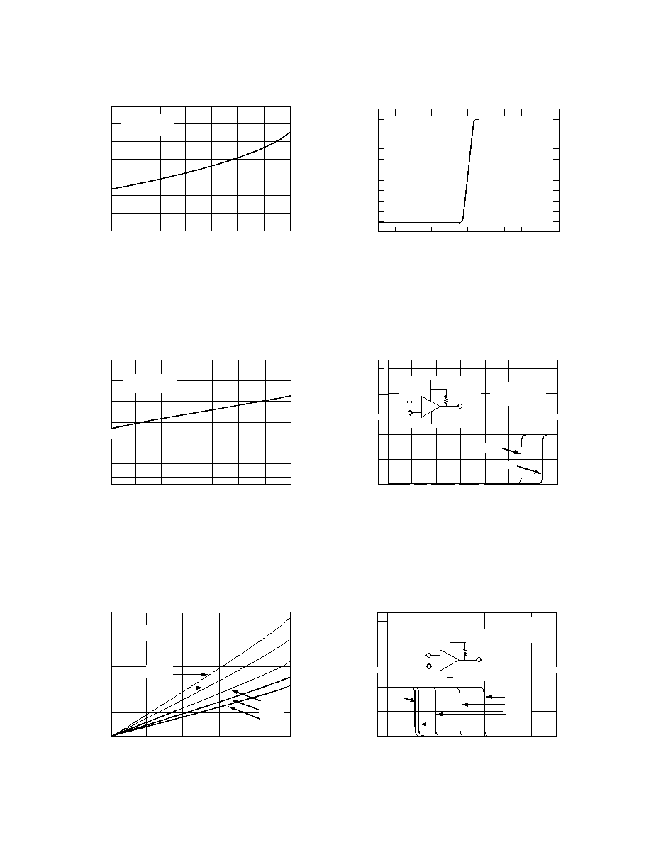
TYPICAL PERFORMANCE CHARACTERISTICS
SATURATION VOLTAGE vs.
SINK CURRENT
OUTPUT SINK CURRENT (mA)
0
15
30
45
60
75
1.5
1.2
0.9
0.6
0.3
0.0
OUTPUT SATURATION
VOLTAGE (V)
V
S
=
±
2.5V
-55
∞
C
25
∞
C
-25
∞
C
85
∞
C
125
∞
C
TIM E (
µ
s)
0
1
2
4
3
6
5
7
RESPONSE TIME FOR VARIOUS
INPUT OVERDRIVES
+2.5
0
100
0.0
-2.5
INPUT
VOLTAGE (mV)
OUTPUT
VOLTAGE (V)
TTL
5mV
10mV
20mV
50mV
T
A
= 25
∞
C
V
S
=
±
2.5V
50K
0V
V
IN
V+
V-
V
OUT
+
-
TRANSFER FUNCTION
DIFFERENTIAL INPUT VOLTAGE (mV)
+6.0
-6.0
0.0
OUTPUT VOLTAGE (V)
+2.5
0.0
-2.5
T
A
= 25
∞
C
V
S
=
±
6V
R
L
= 50K
COMMON - MODE VOLTAGE REFERRED
TO SUPPLY VOLTAGE
TEMPERATURE (
∞
C)
0.5
V+
-0.5
-1.0
0.5
V-
-0.5
COMMON - MODE VOLTAGE LIMITS (V)
-55
-25
0
25
50
125
100
75
V
S
=
±
2.5 V
TIM E (
µ
s)
0
1
2
4
3
6
5
7
RESPONSE TIME FOR VARIOUS
INPUT OVERDRIVES
+2.5
100
0
0.0
-2.5
INPUT
VOLTAGE (mV)
OUTPUT
VOLTAGE (V)
TTL
10mV
T
A
= 25
∞
C
V
S
=
±
2.5V
50K
0V
V
IN
V+
V-
V
OUT
+
-
SATURATION VOLTAGE
vs. TEMPERATURE
TEM PERATURE (
∞
C)
-55
-25
0
25
50
125
100
75
1.4
1.2
1.0
0.8
0.6
0.4
0.2
SATURATION VOLTAGE (V)
0
V
S
=
±
2.5V
I
SINK
= 50mA

ALD2303A/ALD2303
Advanced Linear Devices
16
TYPICAL PERFORMANCE CHARACTERISTICS
10
1
100
6.0
8.0
10.0
12.0
4.0
2.0
SUPPLY VOLTAGE (V)
SUPPLY CURRENT (
µ
A)
-
+
V+
T
A
= 25
∞
C
R
L
=
TOTAL SUPPLY CURRENT vs.
TOTAL SUPPLY VOLTAGE
6
8
10
12
4
2
SUPPLY VOLTAGE (V)
OUTPUT LOW VOLTAGE
vs. SUPPLY VOLTAGE
OUTPUT LOW VOLTAGE (V)
T
A
= 25
∞
C
I
OL
= 12mA
0.0
0.2
0.4
0.5
0.6
0.1
0.3
NORMALIZED INPUT OFFSET VOLTAGE
vs. TEMPERATURE
TEMPERATURE (
∞
C)
+3
+2
+1
0
-1
-2
-3
-55
-25
0
25
50
125
100
75
NORMALIZED INPUT OFFSET
VOLTAGE (mV)
V
CM
= 0V
V
S
=
±
2.5V
0
-2
-4
-6
2
6
8
10
12
4
2
SUPPLY VOLTAGE (V)
6
4
INPUT OFFSET VOLTAGE vs. SUPPLY
VOLTAGE REPRESENTATIVE SAMPLES
INPUT OFFSET VOLTAGE (mV)
T
A
= 25
∞
C
SAMPLES
RESPONSE TIME FOR
REPRESENTATIVE SAMPLES
5
10
0
RESPONSE TIME (
µ
s)
50
100
150
200
V
S
=
±
2.5V
T
A
= 25
∞
C
td
LH
SAMPLES
RESPONSE TIME FOR
REPRESENTATIVE SAMPLES
5
10
0
RESPONSE TIME (
µ
s)
50
100
150
200
V
S
=
±
2.5V
T
A
= 25
∞
C
td
HL
