 | –≠–ª–µ–∫—Ç—Ä–æ–Ω–Ω—ã–π –∫–æ–º–ø–æ–Ω–µ–Ω—Ç: ALD2321SC | –°–∫–∞—á–∞—Ç—å:  PDF PDF  ZIP ZIP |

ULTRA LOW VOS EPAD
Æ
DUAL CMOS ANALOG VOLTAGE COMPARATOR
ALD2321A/ALD2321B
ALD2321
A
DVANCED
L
INEAR
D
EVICES,
I
NC.
ORDERING INFORMATION
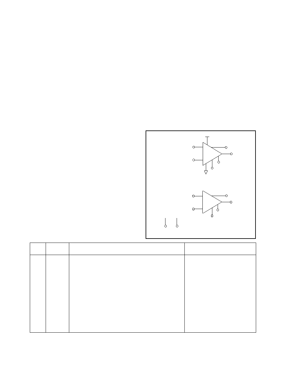
PIN CONFIGURATION
* Contact factory for industrial temperature range
© 2004 Advanced Linear Devices, Inc. 415 Tasman Drive, Sunnyvale, California 94089 -1706 Tel: (408) 747-1155 Fax: (408) 747-1286 http://www.aldinc.com
*N/C pins are connected internally. Do not connect externally.
APPLICATIONS
* Low level signal detector
* Dual limit window comparator
* Power supply voltage monitor
* Photo-detector sensor circuit
* Relay or LED driver
* Oscillators
* Battery operated instruments
* Remote signal detection
Operating Temperature Range*
0
∞
C to +70
∞
C 0
∞
C to +70
∞
C -55
∞
C to +125
∞
C
16-pin
16-Pin 16-Pin
Small Outline Package Plastic DIP Package Ceramic DIP Package
(SOIC)
(PDIP) (CDIP)
ALD2321ASC ALD2321APC ALD2321ADC
ALD2321BSC ALD2321BPC ALD2321BDC
ALD2321SC ALD2321PC ALD2321DC
GENERAL DESCRIPTION
The ALD2321A/ ALD2321B/ ALD2321 is a monolithic Precision Dual
Voltage Comparator, each having integrated dual complementary
output drivers. It is constructed using advanced silicon gate CMOS
technology. Key features of the ALD2321A/ ALD2321B/ ALD2321
include very high input impedance, very low offset voltage utilizing on-
chip e-trim (EPAD
Æ
electronic-trimming) technology, flexible multiple
output configurations and fast response time with small overdrive
voltage. It is designed for ultra low level signal detection from high
impedance sources. For many applications the ALD2321A/ ALD2321B/
ALD2321 can eliminate an input amplification stage, a precision input
bias stage, a signal level shift stage and an output buffer stage, and do
the entire job from low level input signal detection to high output driver
---- all on a single chip.
The input voltage includes ground, making this voltage comparator ideal
for single supply +5V or dual supply +/- 5V powered systems. For dual
supply applications, GND pin is connected to the most negative supply
instead of Ground (0.0V). The negative supply voltage can be at any
value between 0.0V and -5V. Each voltage comparator is individually
trimmed at the factory for minimum offset voltage at ground voltage
potential, making the ALD2321A/ ALD2321B/ ALD2321 at its best offset
voltage and ready to compare very low signal level voltages at or near
ground potential. Typically a signal less than 1 mV can be resolved and
detected reliably without requiring amplification. Sensor or detector
signals with signal power as low as 0.004 pW(4 x 10
-15
Watt) can be
readily detected.
Each voltage comparator has two complementary output pins, one for
Source Output (OUT
H
)and the other for Sink Output (OUT). This dual
complementary output allows maximum circuit design flexibility. The
outputs can be used as Single-Ended Driver, Multiple WIRED-OR
Outputs, Push-Pull Outputs or Complementary Outputs. The Sink
Output can be used as an open drain output, which has current sink
capability of up to 50 mA. It can also be connected to an external voltage
higher or lower than V+, which provide level shift of the output swing
levels from other than V+ to GND.
PRODUCT FEATURES
* Ultra low signal power of 4 fW detectable
* Ultra low offset voltage of max. 0.2 mV
* Ultra low input bias currents of typ. 0.01pA
* Low supply current of 110
µ
A typical
* Virtually eliminates source impedance effects
* Low operating supply voltage of 3V to 10V
* Single +5V and dual supply
±
5V operation
* High speed for both small and large level
signals 300ns typical for TTL inputs
* CMOS, NMOS and TTL compatible
* Each comparator has separate push and pull
outputs
* High output sink current - typically 50mA
* Low supply current spikes
* Fanout of 30 TTL loads
V
+
1
2
3
14
15
16
4
13
5
12
N/C
*
6
7
8
10
11
OUT
1H
-IN
1
OUT
1
VE
11
N/C
*
VE
12
9
VE
22
VE
21
OUT
2H
OUT
2
DC, PC, SC PACKAGE
-IN
2
+IN
2
+IN
1
GND
*
ALD2321A/ALD2321B
Advanced Linear Devices
2
ALD2321
BLOCK DIAGRAM
PIN #
SYMBOL
FUNCTION
SIGNAL PROPAGATION
ALD2321 PIN IDENTIFICATION
1
OUT1
COMPARATOR 1 SINK OUTPUT
OUTPUT
2
OUT1H COMPARATOR 1 SOURCE OUTPUT
OUTPUT
3
-IN1
COMPARATOR 1 INVERTING INPUT
INPUT
4
+IN1
COMPARATOR 1 NON-INVERTING INPUT
INPUT
5
GND
GROUND / V- SUPPLY
-
6
VE11
- VOS E-Trim COMPARATOR 1
INPUT
7
VE12
+ VOS E-Trim COMPARATOR 1
INPUT
8
N/C
No Connect/Do Not connect externally
-
9
N/C
No Connect/Do Not connect externally
-
10
VE22
+VOS E-Trim COMPARATOR 2
INPUT
11
VE21
- VOS E-Trim COMPARATOR 2
INPUT
12
+IN2
COMPARATOR 2 NON-INVERTING INPUT
INPUT
13
-IN2
COMPARATOR 2 INVERTING INPUT
INPUT
14
OUT2H COMPARATOR 2 SOURCE OUTPUT
OUTPUT
15
OUT2
COMPARATOR 2 SINK OUTPUT
OUTPUT
16
V+
V+ SUPPLY
-
The Source Output can source up to 2 mA and can be used to
drive the base terminal of an external NPN bipolar device or the
gate of a N-channel MOSFET device. Alternatively, the two
outputs, Source Output and Sink Output, can be connected
together to form a push-pull output which has the combined
output capabilities of both channels.
In the dual complementary output mode, each comparator can
be used to drive separate loads. Due to the complementary
nature of the two outputs, only one output is active at any a
given time, except for a limited crossover time. When OUT
(sink output) is active ON, the OUT pin is sinking current and
the OUT
H
pin is OFF and in high impedance mode. Con-
versely, if OUT
H
pin is ON and sourcing current, OUT pin is
OFF. To configure push-pull output, simply connect OUT (sink
output) pin to OUT
H
pin.
Since each voltage comparator has its own complementary
outputs, each comparator can be configured to have a different
output type. For example, one comparator output can be
connected as Open Drain output while the other comparator
can be wired as push-pull output. If used to drive capacitive
loads, the output DC current levels are at a very low level, at
essentially leakage current levels, which can be a power saving
feature.
The ALD2321A/ ALD2321B/ ALD2321 can detect and resolve
very low voltage levels at high speed, with little or no overdrive
voltage. Compared with other voltage comparator devices that
require 100 mV overdrive voltages, or multiple stage circuits
that include input preamp, etc., the ALD2321A/ ALD2321B/
ALD2321 can perform all input to output functions in one device
with minimal delay time and with as low as a 1mV signal.
The ALD2321A/ ALD2321B/ ALD2321 is supplied with 4
external e-trim pins, VE11, VE12, VE21 and VE22. These pins
are used for trimming of the voltage comparator offset voltages
GENERAL DESCRIPTION (cont'd)
at the factory, and normally should be left open unconnected.
However, in some cases these pins can be used as positive/
negative feedback pins, since these pins have a positive/
negative factor on the offset voltage. For example, see TYPI-
CAL APPLICATIONS section titled "Voltage Comparator
With Output Feedback to Provide Hysteresis."
In printed circuit board layout, it is suggested that these pins,
along with no connect (N/C) pins 8 and 9, be surrounded with
ground traces to prevent any possible crosstalk and noise
coupling from other signal sources.
Although not required for most applications, if necessary,
small valued capacitors of approximately 1000 pF can be
mounted at these pins to ground to further reduce noise. For
information on customized trimming under different biasing
and power supply conditions, please contact factory.
(1) OUT
1
NONINVERTING INPUT
+IN
1
(4)
INVERTING INPUT
-IN
1
(3)
(16) V
+
(2) OUT
1H
VE
11
GND
(6)
(7) VE
12
(5)
(15) OUT
2
VE
21
INVERTING INPUT
-IN
2
(13)
(14) OUT
2H
VE
22
(11)
(10)
N/C
(8) (9)
N/C
NONINVERTING INPUT
+IN
2
(12)
-
+
-
+

ALD2321A/ALD2321B
Advanced Linear Devices
3
ALD2321
ABSOLUTE MAXIMUM RATINGS
Supply voltage, V+
+10.6V
Differential input voltage range
-0.3V to V+
+0.3V
Power dissipation
600 mW
Operating temperature range PC, SC package
0
∞
C to +70
∞
C
DC package
-55
∞
C to +125
∞
C
Storage temperature range
-65
∞
C to +150
∞
C
Lead temperature, 10 seconds
+260
∞
C
OPERATING ELECTRICAL CHARACTERISTICS
TA = 25
∞
C V+ = +5V unless otherwise specified
Supply Voltage
V+ 3
10 3
10 3
10 V
Supply Current
IS 110 180
110 180
110 180
µ
A No Load
Two Comparators
Voltage Gain
AVD 50 150
50 150
50 150 V/mV RLOAD
15K
Input Offset Voltage
VOS
0.05 0.2
0.2 0.5
0.5 1.0 mV RLOAD
1.5K
Input Offset Current
1
IOS
0.01 20 0.01 20
0.01 20 pA
Input Bias Current
1
IB 0.01 20 0.01 20
0.01 20 pA
Common Mode Input VICR -0.3
V+ -1.5 -0.3 V+ -1.5 -0.3 V+ -1.5 V
Voltage Range
2
Low Level Sink
VOL
0.15 0.4
0.15 0.4
0.15 0.4 V
ISINK = 12mA
Output Voltage
VINPUT = 1V Differential
Low Level Sink
IOL 24 50
24 50
24
50
mA VOL = 1.0 V
Output Current
SINK OUTPUT ON
High Level Source VOH 3.5 4.5 3.5 4.5 3.5 4.5
V
ISOURCE = -2mA
Output Voltage
SOURCE OUTPUT ON
Source Output Leakage IHL
0.01 1
0.01 1
0.01 1 nA VOH = 0.0V
Current
SOURCE OUTPUT OFF
Sink Output Leakage IL 0.01 20
0.01 20
0.01 20 nA VOUT = 5.0 V
Current
SINK OUTPUT OFF
Response Time
2
tRP
1.1
1.1
1.1
µ
s
RL = 5.1K
, CL = 15pF
5mV Input Step/
0mV Overdrive
tRP
2.4
2.4
2.4
µ
s
RL = 5.1K
,CL =15pF
1mVInput Step/
0mV Overdrive
Common Mode CMRR
80
80
80
dB VINPUT = 0V to 2.5V
Rejection Ratio
Power Supply Rejection PSRR
75
75
75
dB V+ = 4V to 5V
Ratio
Change of Vos / VExx
VOS
5
5
5
mV/V VE pins No Load
VE
2321A
2321B 2321
Parameter
Symbol Min Typ Max Min Typ Max Min Typ Max Unit Test Conditions
Notes:
1
Consists of junction leakage currents
2
Sample test parameter
ALD2321A/ALD2321B
Advanced Linear Devices
4
ALD2321
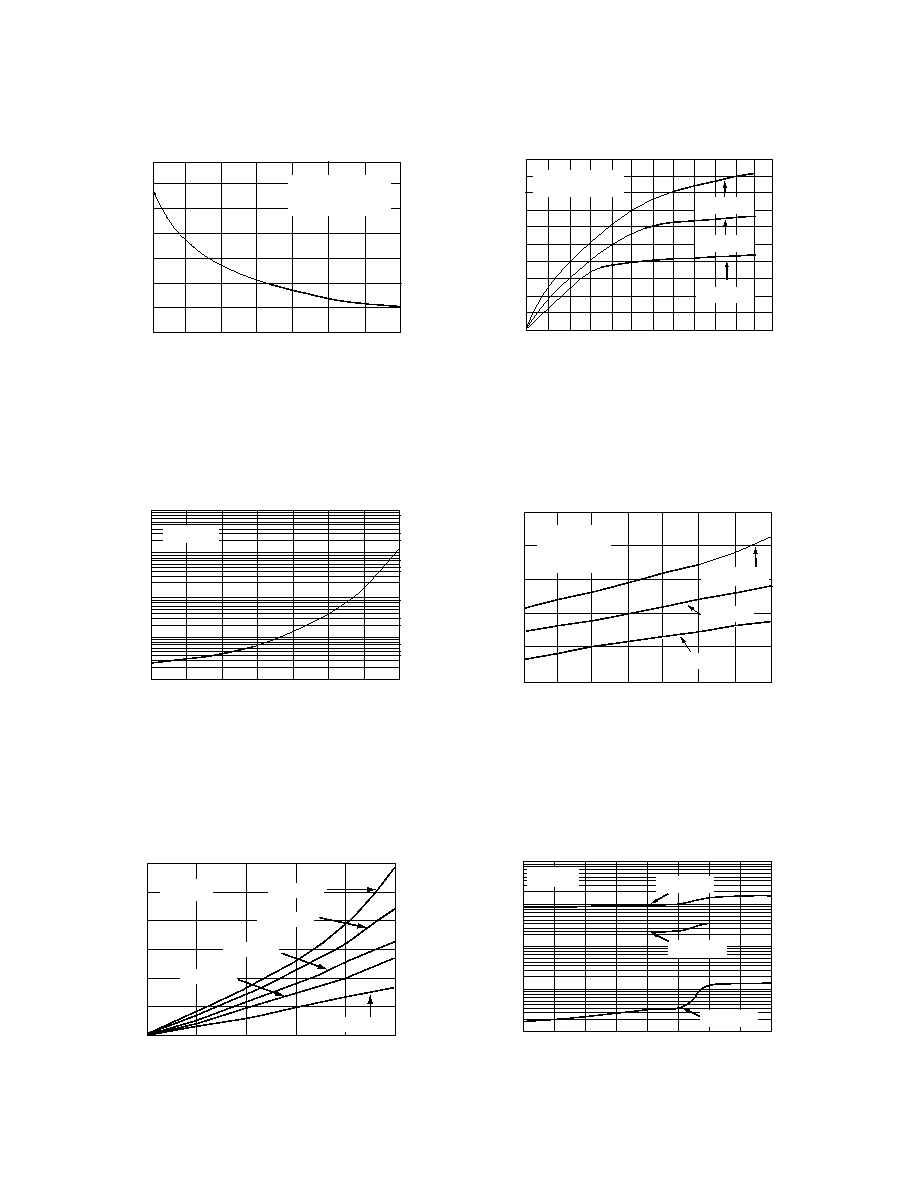
TYPICAL PERFORMANCE CHARACTERISTICS
SUPPLY CURRENT vs.TEMPERATURE
SUPPLY CURRENT (
µ
A)
AMBIENT TEMPERATURE (
∞
C)
-55
-25
0
25
50
125
100
75
160
140
120
100
60
80
180
200
V
+
= +5V
No Load
Two Comparators
SUPPLY CURRENT vs. SUPPLY VOLTAGE
0
12
200
SUPPLY VOLTAGE (V)
SUPPLY CURRENT (
µ
A)
0
10
8
6
2
4
20
40
60
80
100
120
140
160
180
No Load
Two Comparators
T
A
= 25
0
C
T
A
= 125
0
C
T
A
= -55
0
C
-55
-25
0
25
50
75
100
125
0
1
10
100
1000
V
+
= +5V
INPUT BIAS CURRENT vs. TEMPERATURE
AMBIENT TEMPERATURE (
0
C)
INPUT BIAS CURRENT (pA)
LOW LEVEL OUTPUT VOLTAGE
vs. TEMPERATURE
0.5
0.4
0.3
0.2
0.1
0.0
LOW LEVEL OUTPUT VOLTAGE (V)
AMBIENT TEMPERATURE (
∞
C)
-55
-25
0
25
50
125
100
75
V
+
= +3.5V
V
+
= +5V
V
+
= +10V
I
SINK = 12mA
V
INPUT =
1V
Differential
SATURATION VOLTAGE vs. SINK CURRENT
OUTPUT SINK CURRENT (mA)
0
15
30
45
60
75
OUTPUT SATURATION VOLTAGE (V)
3.0
2.0
1.0
0.0
2.5
1.5
0.5
V
+
= +5V
T
A
= 125
0
C
T
A
= -55
0
C
T
A
= 85
0
C
T
A
= 25
0
C
T
A
= -25
0
C
HIGH LEVEL OUTPUT VOLTAGE vs. HIGH
LEVEL OUTPUT LEAKAGE CURRENT
3
4
5
6
7
8
9
10
11
0.0
0.1
1.0
10.0
100.0
V
OH
= V
+
HIGH LEVEL OUTPUT CURRENT (nA)
HIGH LEVEL OUTPUT VOLTAGE (V)
T
A
= 125
0
C
T
A
= 85
0
C
T
A
= 25
0
C
ALD2321A/ALD2321B
Advanced Linear Devices
5
ALD2321
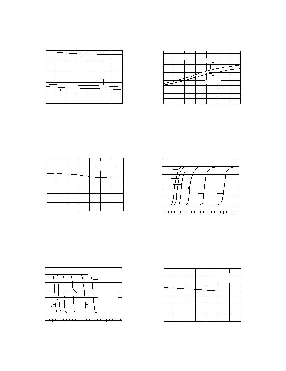
TYPICAL PERFORMANCE CHARACTERISTICS
COMMON MODE REJECTION RATIO
vs. TEMPERATURE
COMMON MODE REJECTION MODE
(dB)
-55
-25
0
25
50
125
100
75
85.0
80.0
75.0
70.0
90.0
65.0
60.0
AMBIENT TEMPERATURE (
∞
C)
V
+
= +5V
R
L
= 5.1K
POWER SUPPLY REJECTION RATIO
vs.TEMPERATURE
AMBIENT TEMPERATURE (
0
C)
-55
-25
0
25
50
100
125
75
90.0
85.0
70.0
POWER SUPPLY REJECTION RATIO
(dB)
80.0
75.0
65.0
60.0
V
+
= +5V
R
L
= 5.1K
HIGH LEVEL OUTPUT VOLTAGE vs.
TEMPERATURE
8.0
6.0
4.0
0.0
HIGH LEVEL OUTPUT VOTAGE (V)
AMBIENT TEMPERATURE (
∞
C)
-55
-25
0
25
50
125
100
75
2.0
10.0
V
+
= +10V
V
+
= +5V
V
+
= +4V
I
OH
= -2mA
INPUT OFFSET VOLTAGE vs. TEMPERATURE
0.4
0.0
-0.4
0.8
-0.8
-1.2
1.2
-2.0
INPUT OFFSET VOLTAGE (mV)
-55
-25
0
25
50
125
100
75
AMBIENT TEMPERATURE (
∞
C)
-1.6
2.0
1.6
R
L
= 5.1K
V
+
= +5V
V
+
= +2.5V
RESPONSE TIME FOR VARIOUS INPUT
OVERDRIVES
OUTPUT VOLTAGE
(V)
-1.0
6.0
2.0
0.0
1.0
3.0
4.0
5.0
0.0 0.3 0.6
0.9
1.2 1.5
1.8
2.1 2.4 2.7
3.0
TIME (
µ
S)
T
A
= 25
0
C
V
+
= +5V
1mV
2mV
5mV
10mV
20mV
50mV
R
L
= 5.1K
C
L
= 15pF
Input Step
0.0
0.3
0.6
0.9
1.2
1.5
1.8
2.1
2.4
2.7
3.0
-1.0
0.0
1.0
2.0
3.0
4.0
5.0
6.0
RESPONSE TIME FOR VARIOUS INPUT
OVERDRIVES
OUTPUT VOLTAGE
(V)
TIME (
µ
S)
50mV
20mV
10mV
5mV 2mV
1mV
V
+
= +5V
R
L
= 5.1K
Input Step
C
L
= 15pF
T
A
= 25
0
C