APPLICATIONS
∑ Voltage follower/buffer
∑ Charge integrator
∑ Photodiode amplifier
∑ Data acquisition systems
∑ High performance portable instruments
∑ Signal conditioning circuits
∑ Sensor and transducer amplifiers
∑ Low leakage amplifiers
∑ Active filters
∑ Sample/Hold amplifier
∑ Picoammeter
∑ Current to voltage converter
∑ Coaxial cable driver
DUAL 5V RAIL-TO-RAIL PRECISION OPERATIONAL AMPLIFIER
A
DVANCED
L
INEAR
D
EVICES,
I
NC.
ALD2702A/ALD2702B
ALD2702
GENERAL DESCRIPTION
The ALD2702 is a dual monolithic operational amplifier intended primarily
for a wide range of analog applications in +5V single power supply and
±
5V
dual power supply systems as well as +4V to +12V battery operated
systems. All device characteristics are specified for +5V single supply or
±
2.5V dual supply systems. The device has an input stage that operates to
+300mV above and -300mV below the supply voltages with no adverse
effects and/or phase reversals. It offers popular industry pin configuration.
The ALD2702 has been developed specifically with the +5V single supply
or
±
2.5V dual supply user in mind. Several important characteristics of the
device make many applications easy to implement for these supply
voltages. First, the operational amplifier can operate with rail to rail input
and output voltages. This feature allows numerous analog serial stages to
be implemented without losing operating voltage margin. Secondly, the
device was designed to accommodate mixed applications where digital
and analog circuits may work off the same 5V power supply. Thirdly, the
output stage can drive up to 400pF capacitive and 5K
resistive loads in
non-inverting unity gain connection and double the capacitance in the
inverting unity gain mode.
These features, coupled with extremely low input currents, high voltage
gain, useful bandwidth of 1.5MHz, a slew rate of 1.9V/
µ
s, low power
dissipation, low offset voltage and temperature drift, make the ALD2702 a
truly versatile, user friendly, operational amplifier.
The ALD2702 is designed and fabricated with silicon gate CMOS technology,
and offers less than 1pA typical input bias current. On-chip offset voltage
trimming allows the device to be used without nulling in most applications.
The device offers typical offset drift of less than 7
µ
V/
∞
C which eliminates
many trim or temperature compensation circuits. For precision applications,
the ALD2702 is designed to settle to 0.01% in 8
µ
s.
FEATURES
∑ Rail-to-rail input and output voltage range
∑ Symmetrical push-pull class AB output
drivers
∑ All parameters specified for +5V single
supply or
±
2.5V dual supply systems
∑ High load capacitance capability -- drives
up to 4000pF typical
∑ No frequency compensation required --
unity gain stable
∑ Extremely low input bias currents --
<1.0pA typical
∑ Ideal for high source impedance applications
∑ Dual power supply
±
2.5V to
±
6V operation
∑ Single power supply +5V to +12V operation
∑ High voltage gain -- typically 85V/mV
@
±
2.5V and 250V/mV @
±
5.0V
∑ Drive as low as 2K
load with 5mA
drive current
∑ Output short circuit protected
∑ Unity gain bandwidth of 1.5MHz
∑ Slew rate of 1.9V/
µ
s
∑ Low power dissipation
ORDERING INFORMATION
Operating Temperature Range *
-55
∞
C to +125
∞
C
0
∞
C to +70
∞
C
0
∞
C to +70
∞
C
8-Pin
8-Pin
8-Pin
CERDIP
Small Outline
Plastic Dip
Package
Package (SOIC)
Package
ALD2702A DA
ALD2702A SA
ALD2702A PA
ALD2702B DA
ALD2702B SA
ALD2702B PA
ALD2702 DA
ALD2702 SA
ALD2702 PA
* Contact factory for industrial temperature range
PIN CONFIGURATION
1
2
3
4
8
7
6
5
TOP VIEW
DA, PA, SA PACKAGE
OUT A
-IN A
+IN A
V+
-IN B
+IN B
V -
OUT B
© 1998 Advanced Linear Devices, Inc. 415 Tasman Drive, Sunnyvale, California 94089 -1706 Tel: (408) 747-1155 Fax: (408) 747-1286 http://www.aldinc.com
ALD2702A/ALD2702B
Advanced Linear Devices
2
ALD2702
ABSOLUTE MAXIMUM RATINGS
Supply voltage, V
+
referenced to V
-
-0.3V to V++13.2V
Supply voltage, V
S
referenced to V
-
±
6.6V
Differential input voltage range
0.3V to V+
+0.3V
Power dissipation
600 mW
Operating temperature range PA, SA package
0
∞
C to +70
∞
C
DA package
-55
∞
C to +125
∞
C
Storage temperature range
-65
∞
C to +150
∞
C
Lead temperature, 10 seconds
+260
∞
C
Supply
V
S
±
2.0
±
6.0
±
2.0
±
6.0
±
2.0
±
6.0
V
Voltage
V
+
4.0
12.0
4.0
12.0
4.0
12.0
V
Single Supply
Input Offset
V
OS
1.0
2.0
5.0
mV
R
S
100K
Voltage
1.5
3.0
6.0
mV
0
∞
C
T
A
+70
∞
C
Input Offset
I
OS
1.0
20
1.0
20
1.0
20
pA
T
A
= 25
∞
C
Current
240
240
240
pA
0
∞
C
T
A
+70
∞
C
Input Bias
I
B
1.0
20
1.0
20
1.0
20
pA
T
A
= 25
∞
C
Current
300
300
300
pA
0
∞
C
T
A
+70
∞
C
Input Voltage
V
IR
-0.3
5.3
-0.3
5.3
-0.3
5.3
V
V
+
= +5V
Range
-2.8
+2.8
-2.8
+2.8
-2.8
+2.8
V
V
S
=
±
2.5V
Input
R
IN
10
12
10
12
10
12
Resistance
Input Offset
TCV
OS
7
7
7
µ
V/
∞
C
R
S
100K
Voltage Drift
Power Supply
PSRR
65
83
65
83
63
83
dB
R
S
100K
Rejection Ratio
65
83
65
83
63
83
0
∞
C
T
A
+70
∞
C
Common Mode
CMRR
65
83
65
83
63
83
dB
R
S
100K
Rejection Ratio
65
83
65
83
63
83
0
∞
C
T
A
+70
∞
C
Large Signal
A
V
15
28
15
28
12
28
V/mV
R
L
= 10K
Voltage Gain
100
100
100
V/mV
R
L
1M
Output
V
O
low
0.002
0.01
0.002 0.01
0.002
0.01
R
L
= 1M
Single supply
Voltage
V
O
high
4.99
4.998
4.99
4.998
4.99 4.998
V
0
∞
C
T
A
+70
∞
C
Range
V
O
low
-2.44
-2.40
-2.44 -2.40
-2.44
-2.40
V
R
L
= 10K
Dual supply
V
O
high
2.40
2.44
2.40
2.44
2.40
2.44
V
0
∞
C
T
A
+70
∞
C
Output Short
I
SC
8
8
8
mA
Circuit Current
Supply
I
S
2.0
3.0
2.0
3.0
2.0
3.0
mA
V
IN
= 0V No Load
Current
Power
P
D
10
15.0
10
15.0
10
15.0
mW
Both amplifiers
Dissipation
V
S
=
±
2.5V
Input
C
IN
1
1
1
pF
Capacitance
Bandwidth
B
W
0.7
1.5
0.7
1.5
0.7
1.5
MHz
Slew Rate
S
R
1.1
1.9
1.1
1.9
1.1
1.9
V/
µ
s
A
V
= +1 R
L
= 10K
Rise time
t
r
0.2
0.2
0.2
µ
s
R
L
= 10K
Overshoot
10
10
10
%
R
L
= 10K
C
L
= 100pF
Factor
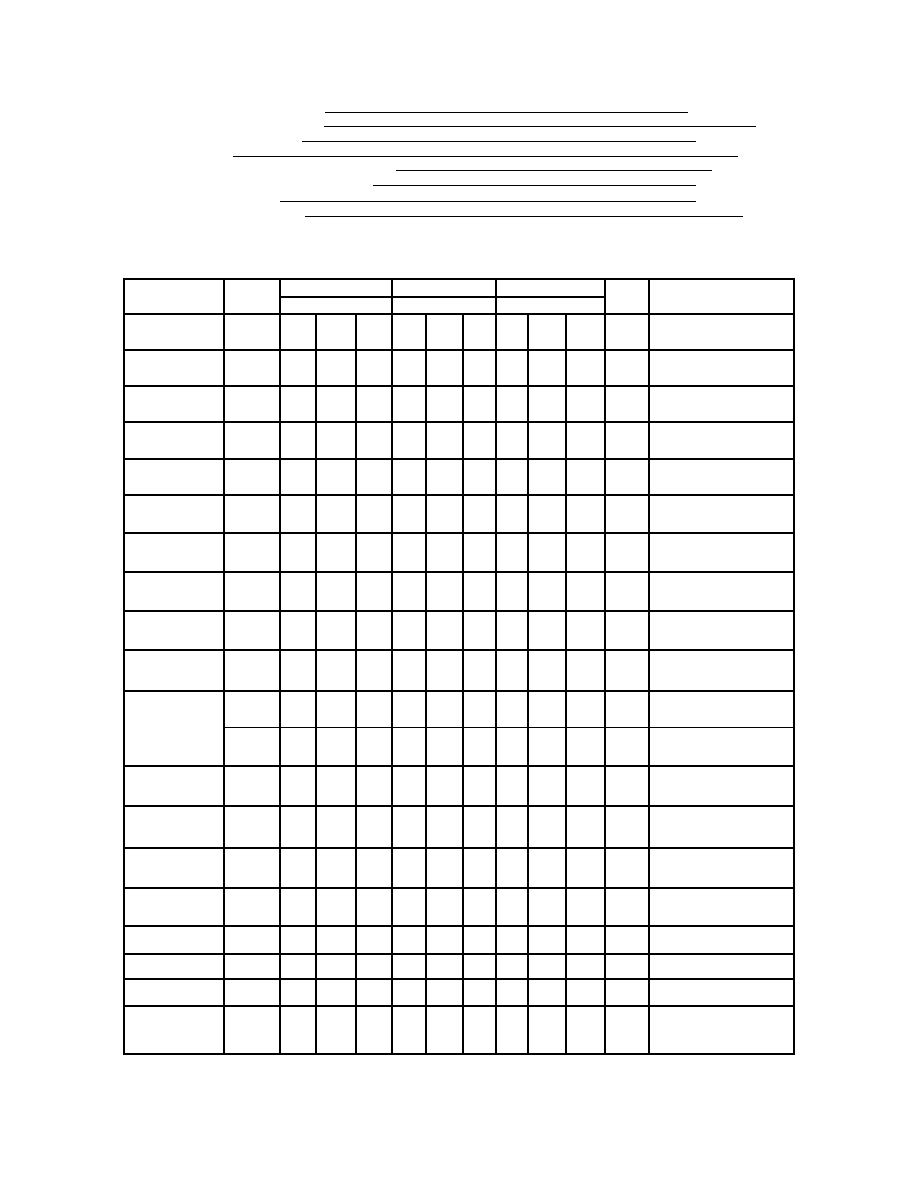
OPERATING ELECTRICAL CHARACTERISTICS
T
A
= 25
∞
C V
S
=
±
2.5V unless otherwise specified
2702A 2702B 2702
Test
Parameter
Symbol
Min
Typ
Max
Min
Typ
Max
Min
Typ
Max
Unit
Conditions
ALD2702A/ALD2702B
Advanced Linear Devices
3
ALD2702
Maximum Load
C
L
400
400
400
pF
Gain = 1
Capacitance
4000
4000
4000
pF
Gain = 5
Input Noise
e
n
26
26
26
nV/
H
Z
f = 1KH
Z
Voltage
Input Current
i
n
0.6
0.6
0.6
fA/
H
Z
f = 10H
Z
Noise
Settling
t
s
8.0
8.0
8.0
µ
s
0.01%
Time
3.0
3.0
3.0
µ
s
0.1% A
V
= -1
R
L
= 5K
C
L
= 50pF
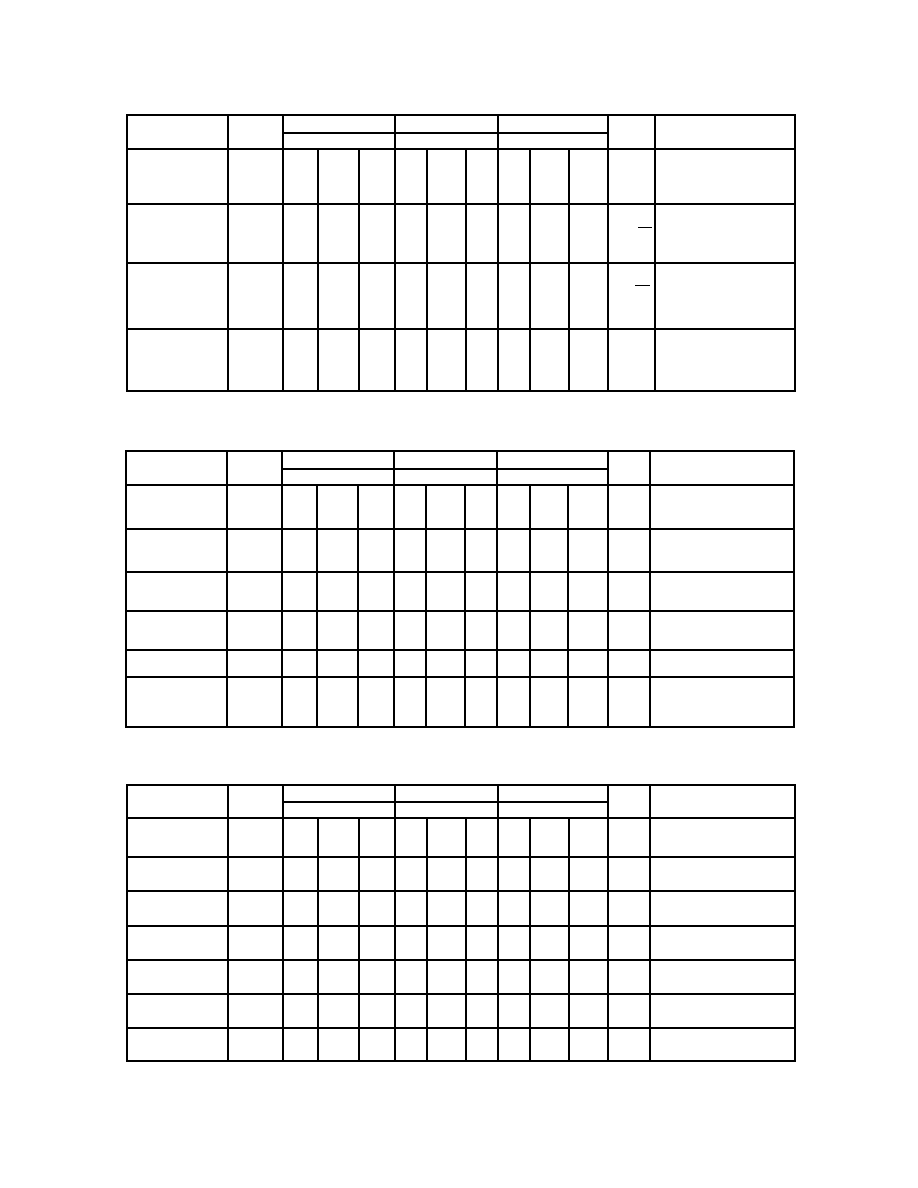
OPERATING ELECTRICAL CHARACTERISTICS (cont'd)
T
A
= 25
∞
C V
S
=
±
2.5V unless otherwise specified
2702A
2702B
2702
Parameter
Symbol
Min
Typ
Max
Min
Typ
Max
Min
Typ
Max
Unit
Test Conditions
T
A
= 25
∞
C V
S
=
±
5.0V unless otherwise specified
2702A
2702B
2702
Parameter
Symbol
Min
Typ
Max
Min
Typ
Max
Min
Typ
Max
Unit
Test Conditions
Power Supply
PSRR
83
83
83
dB
R
S
100K
Rejection Ratio
Common Mode
CMRR
83
83
83
dB
R
S
100K
Rejection Ratio
Large Signal
A
V
250
250
250
V/mV
R
L
= 10K
Voltage Gain
Output Voltage
V
O
low
-4.90
-4.8
-4.90
-4.8
-4.90
-4.8
V
R
L
= 10K
Range
V
O
high
4.8
4.93
4.8
4.93
4.8
4.93
Bandwidth
B
W
1.7
1.7
1.7
MH
Z
Slew Rate
S
R
2.8
2.8
2.8
V/
µ
s
A
V
=+1
C
L
=50pF
Input Offset
V
OS
2.0
4.0
7.0
mV
R
S
100K
Voltage
Input Offset
I
OS
8.0
8.0
8.0
nA
Current
Input Bias
I
B
10.0
10.0
10.0
nA
Current
Power Supply
PSRR
60
75
60
75
60
75
dB
R
S
100K
Rejection Ratio
Common Mode
CMRR
60
83
60
83
60
83
dB
R
S
100K
Rejection Ratio
Large Signal
A
V
10
25
10
25
7
25
V/mV
R
L
10K
Voltage Gain
Output Voltage
V
O
low
0.1
0.2
0.1
0.2
0.1
0.2
V
R
L
10K
Range
V
O
high
4.8
4.9
4.8
4.9
4.8
4.9
V
S
= +5.0V -55
∞
C
T
A
+125
∞
C unless otherwise specified
2702A DA
2702B DA
2702 DA
Parameter
Symbol
Min
Typ
Max
Min
Typ
Max
Min
Typ
Max
Unit
Test Conditions
ALD2702A/ALD2702B
Advanced Linear Devices
4
ALD2702
Design & Operating Notes:
1. The ALD2702 CMOS operational amplifier uses a 3 gain stage
architecture and an improved frequency compensation scheme to
achieve large voltage gain, high output driving capability, and
better frequency stability. The ALD2702 is internally compensated
for unity gain stability using a novel scheme. This design produces
a clean single pole roll off in the gain characteristics while providing
for more than 70 degrees of phase margin at the unity gain
frequency. A unity gain buffer using the ALD2702 will typically
drive 400pF of external load capacitance without stability problems.
In the inverting unity gain configuration, it can drive up to 800pF
of load capacitance. Compared to other CMOS operational
amplifiers, the ALD2702 has shown itself to be more resistant to
parasitic oscillations.
2. The ALD2702 has complementary p-channel and n-channel input
differential stages connected in parallel to accomplish rail-to-rail input
common mode voltage range. With the common mode input voltage
close to the power supplies, one of the two differential stages is
switched off internally. To maintain compatibility with other operational
amplifiers, this switching point has been selected to be about 1.5V
above the negative supply voltage. As offset voltage trimming on the
ALD2702 is made when the input voltage is symmetrical to the supply
voltages, this internal switching does not affect a large variety of
applications such as an inverting amplifier or non-inverting amplifier
with a gain greater than 2.5 (5V operation), where the common mode
voltage does not make excursions below this switching point.
3. The input bias and offset currents are essentially input protection
diode reverse bias leakage currents, and are typically less than 1pA
at room temperature. This low input bias current assures that the
analog signal from the source will not be distorted by input bias
currents. For applications where source impedance is very high, it may
be necessary to limit noise and hum pickup through proper shielding.
4. The output stage consists of class AB complementary output drivers,
capable of driving a low resistance load. The output voltage swing is
limited by the drain to source on-resistance of the output transistors
as determined by the bias circuitry, and the value of the load resistor.
When connected in the voltage follower configuration, the oscillation
resistant feature, combined with the rail to rail input and output feature,
makes the ALD2702 an effective analog signal buffer for medium to
high source impedance sensors, transducers, and other circuit
networks.
5. The ALD2702 operational amplifier has been designed with static
discharge protection. Internally, the design has been carefully
implemented to minimize latch up. However, care must be exercised
when handling the device to avoid strong static fields. In using the
operational amplifier, the user is advised to power up the circuit before,
or simultaneously with, any input voltages applied and to limit input
voltages to not exceed 0.3V of the power supply voltage levels.
Alternatively, a 100K
or higher value resistor at the input terminals
will limit input currents to acceptable levels while causing very small
or negligible accuracy effects.
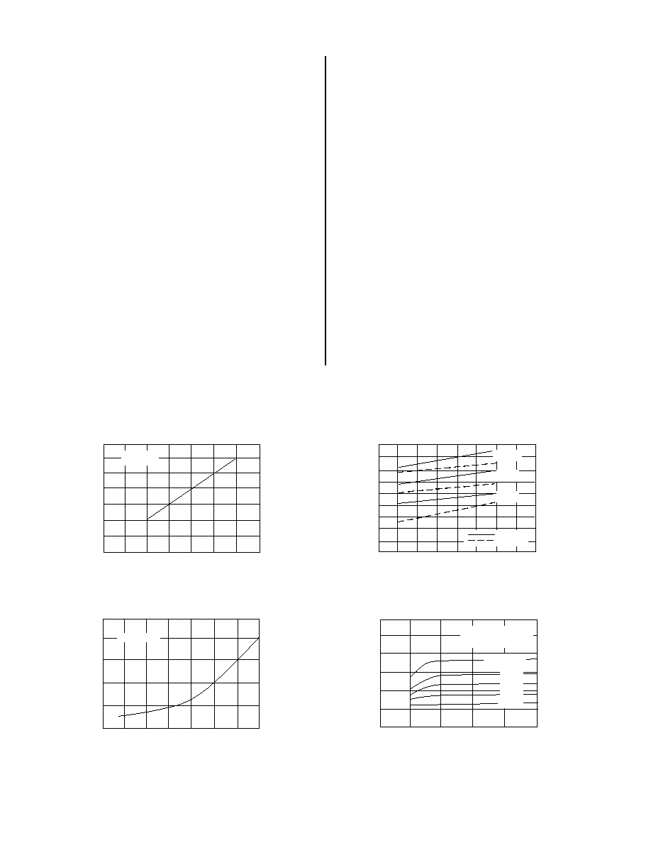
TYPICAL PERFORMANCE CHARACTERISTICS
INPUT BIAS CURRENT AS A FUNCTION
OF AMBIENT TEMPERATURE
AMBIENT TEMPERATURE (
∞
C)
1000
100
10
0.1
1.0
INPUT BIAS CURRENT (pA)
100
-25
0
75
125
50
25
-50
V
S
=
±
2.5V
10000
OPEN LOOP VOLTAGE GAIN AS A FUNCTION
OF SUPPLY VOLTAGE AND TEMPERATURE
SUPPLY VOLTAGE (V)
1000
100
10
1
OPEN LOOP VOLTAGE
GAIN (V/mV)
0
±
2
±
4
±
6
R
L
= 10K
R
L
= 5K
} -55
∞
C
} +25
∞
C
} +125
∞
C
±
8
SUPPLY CURRENT AS A FUNCTION
OF SUPPLY VOLTAGE
SUPPLY VOLTAGE (V)
SUPPLY CURRENT (mA)
6
5
4
3
1
2
0
±
6
±
5
±
4
±
3
±
1
±
2
INPUTS GROUNDED
OUTPUTS UNLOADED
T
A
= -55
∞
C
-25
∞
C
+80
∞
C
+125
∞
C
+25
∞
C
COMMON MODE INPUT VOLTAGE RANGE
AS A FUNCTION OF SUPPLY VOLTAGE
SUPPLY VOLTAGE (V)
COMMON MODE INPUT
VOLTAGE RANGE (V)
±
7
±
6
±
5
±
4
±
3
±
2
±
1
0
0
±
1
±
2
±
3
±
4
±
5
±
6
±
7
T
A
= 25
∞
C
ALD2702A/ALD2702B
Advanced Linear Devices
5
ALD2702
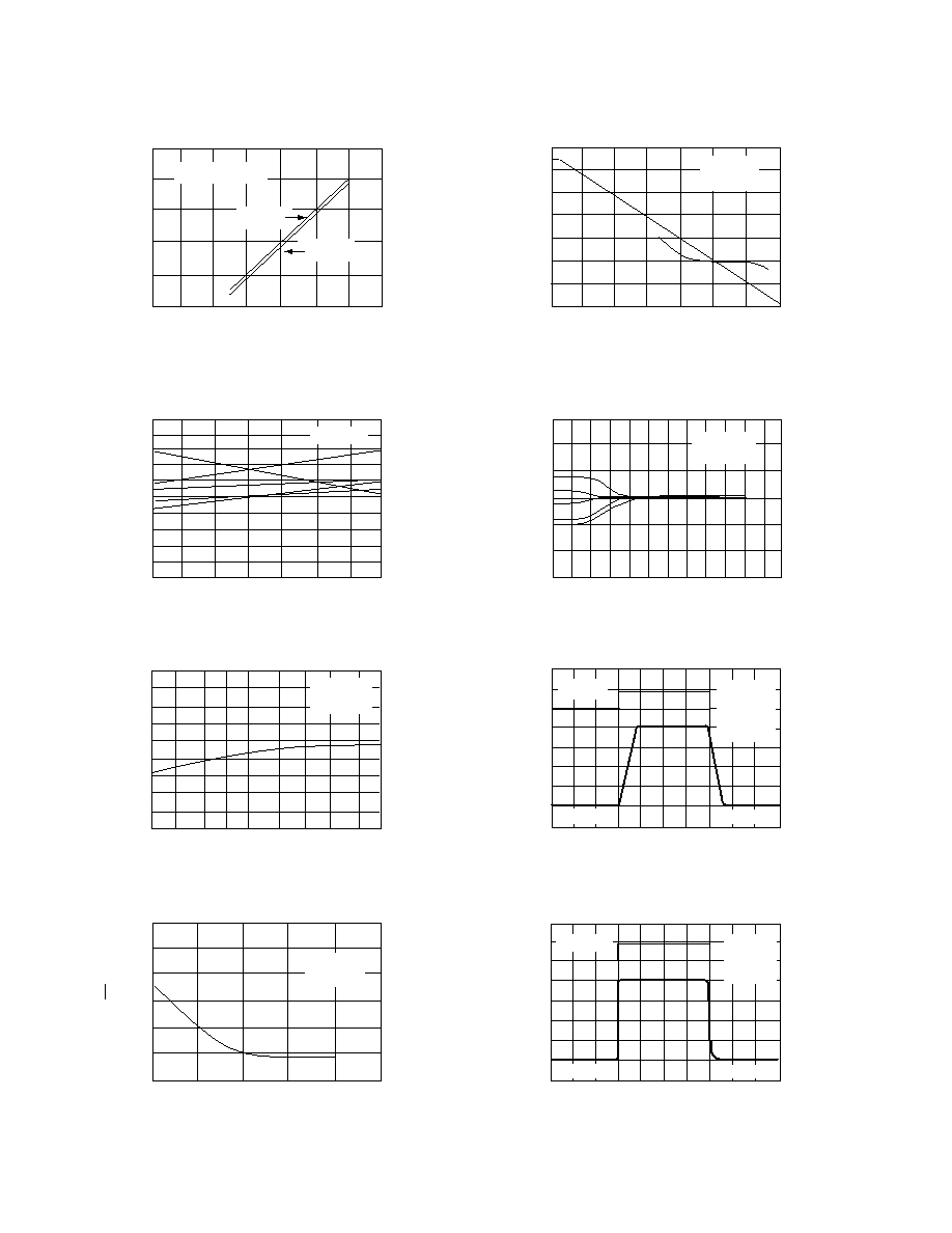
TYPICAL PERFORMANCE CHARACTERISTICS
LARGE - SIGNAL TRANSIENT
RESPONSE
5V/div
1V/div
2
µ
s/div
V
S
=
±
2.5V
T
A
= 25
∞
C
R
L
= 10K
C
L
= 50pF
SMALL - SIGNAL TRANSIENT
RESPONSE
100mV/div
20mV/div
V
S
=
±
2.5V
T
A
= 25
∞
C
R
L
= 10K
C
L
= 50pF
2
µ
s/div
INPUT OFFSET VOLTAGE AS A FUNCTION
OF AMBIENT TEMPERATURE
REPRESENTATIVE UNITS
AMBIENT TEMPERATURE (
∞
C)
INPUT OFFSET VOLTAGE (mV)
-50
-25
0
+25
+50
+75
+100 +125
+4
+5
+3
+1
+2
0
-2
-1
-4
-3
-5
V
S
=
±
2.5V
INPUT OFFSET VOLTAGE AS A FUNCTION
OF COMMON MODE INPUT VOLTAGE
COMMON MODE INPUT VOLTAGE (V)
-2
-1
0
+1
+2
+3
15
10
5
0
-5
-10
-15
INPUT OFFSET VOLTAGE (mV)
V
S
=
±
2.5V
T
A
= 25
∞
C
OPEN LOOP VOLTAGE GAIN AS A
FUNCTION OF LOAD RESISTANCE
LOAD RESISTANCE (
)
1K
10K
1000K
100K
1000
100
10
1
OPEN LOOP VOLTAGE GAIN (V/mV)
V
S
=
±
2.5V
T
A
= 25
∞
C
OPEN LOOP VOLTAGE GAIN AS
A FUNCTION OF FREQUENCY
FREQUENCY (Hz)
1
10
100
1K
10K
1M
10M
100K
120
100
80
60
40
20
0
-20
OPEN LOOP VOLTAGE
GAIN (dB)
V
S
=
±
2.5V
T
A
= 25
∞
C
90
0
45
180
135
PHASE SHIFT IN DEGREES
VOLTAGE NOISE DENSITY AS A
FUNCTION OF FREQUENCY
FREQUENCY (Hz)
10
100
1K
10K
100K
150
125
100
75
50
25
0
1000K
VOLTAGE NOISE DENSITY
(nV/
Hz)
V
S
=
±
2.5V
T
A
= 25
∞
C
RL = 10K
OUTPUT VOLTAGE SWING AS A
FUNCTION OF SUPPLY VOLTAGE
SUPPLY VOLTAGE (V)
OUTPUT VOLTAGE SWING (V)
±
3
0
±
1
±
2
±
3
±
4
±
5
±
6
±
7
R
L
= 2K
±
6
±
5
±
4
±
2
±
7
±
25
∞
C
T
A
125
∞
C
R
L
= 10K