Operating Temperature Range *
-55
∞
C to +125
∞
C
0
∞
C to +70
∞
C
0
∞
C to +70
∞
C
14-Pin
14-Pin
14-Pin
CERDIP
Small Outline
Plastic Dip
Package
Package (SOIC)
Package
ALD4303ADB
ALD4303ASB
ALD4303APB
ALD4303DB
ALD4303SB
ALD4303PB
QUAD PRECISION MICROPOWER CMOS VOLTAGE COMPARATOR WITH DRIVER
ALD4303A/ALD4303
ORDERING INFORMATION
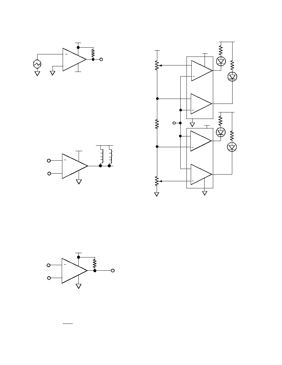
APPLICATIONS
∑ Sensor detection circuits
∑ PCMCIA instruments
∑ MOSFET driver
∑ High source impedance voltage comparison circuits
∑ Multiple limit window comparator
∑ Power supply voltage monitor
∑ Photodetector sensor circuit
∑ High speed LED driver
∑ Oscillators
∑ Battery operated instruments
∑ Remote signal detection
∑ Multiple relay drivers
BENEFITS
∑ Extremely low power and high precision combination
∑ Built-in high input impedance buffer
∑ Built-in output driver with up to 60mA sink current
A
DVANCED
L
INEAR
D
EVICES,
I
NC.
FEATURES
∑ 3V, 5V and 12V supply
∑ Guaranteed to drive 200
loads
∑ Fanout of 30LS TTL loads
∑ Guaranteed maximum supply current of
22
µ
A per comparator
∑ Industry standard pinout of LM393 type
∑ Extremely low input bias currents -- 10pA
∑ Virtually eliminates source impedance
effects
∑ Single (+5V) and dual supply (
±
5V)
operation
∑ CMOS, NMOS and TTL compatible
∑ Open drain wired-OR outputs
∑ Compatible with push-pull outputs
∑ High output sinking current -- 60mA
∑ Low supply current spikes
∑ High gain -- 100V/mV
GENERAL DESCRIPTION
The ALD4303A/ALD4303 is a precision monolithic high performance
quad voltage comparator with open drain output built with advanced
silicon gate CMOS technology. It features very high typical input
impedance of 10
12
; low input bias current of 10pA; very low power
dissipation of 7.5
µ
A per comparator; micropower operation; high
output drive and single (+5V) or dual (
±
5V) power supply operation.
The input voltage range includes ground, making this comparator ideal
for single supply low level signal detection with high source impedance.
The ALD4303A/ALD4303 can be used in connection with other voltage
comparator circuits such as the ALD2301/ALD2302/ALD4302 voltage
comparators. The outputs can be connected to a higher external
voltage than V
+
and used in a wired-OR connection with other open
drain circuits such as ALD2301/ALD2303. They can also be used with
push-pull output types such as ALD2302/ALD4302 voltage compara-
tors simultaneously with open drain comparators using a common V+.
The ALD4303A/ALD4303 is ideal for a great variety of voltage com-
parator applications, especially micropower detection circuits requiring
very low input currents, high output currents and low standby power.
* Contact factory for industrial temperature range
PIN CONFIGURATION
BLOCK DIAGRAM
© 2005 Advanced Linear Devices, Inc. 415 Tasman Drive, Sunnyvale, California 94089 -1706 Tel: (408) 747-1155 Fax: (408) 747-1286 http://www.aldinc.com
DB, PB, SB PACKAGE
+IN
1
-IN
2
+IN
2
03
04
GND
-IN
4
+IN
3
-IN
3
02
01
-IN
1
+IN
4
1
14
V
+
2
3
13
12
11
10
9
8
4
5
6
7
V
+
(3)
INVERTING INPUT
- IN
1
(4)
NONINVERTING INPUT
+ IN
1
(5)
NONINVERTING INPUT
+ IN
2
(7)
INVERTING INPUT
- IN
2
(6)
NONINVERTING INPUT
+ IN
3
(9)
INVERTING INPUT
- IN
3
(8)
INVERTING INPUT
- IN
4
(10)
(12)
NONINVERTING INPUT
+ IN
4
(11)
-
+
-
+
-
+
-
+
(2) OUT
1
(1) OUT
2
(14) OUT
3
(13) OUT
4

ALD4303A/ALD4303
Advanced Linear Devices
OPERATING ELECTRICAL CHARACTERISTICS
T
A
= 25
∞
C V+= +5V unless otherwise specified
4303A
4303
Test
Parameter
Symbol
Min
Typ
Max
Min
Typ
Max
Unit
Conditions
Notes:
1
Consists of junction leakage currents
2
Sample tested parameters
Voltage
V
S
±
1.5
±
6
±
1.5
±
6
V
Dual Supplies
Supply
V
+
3
12
3
12
V
Single Supply
Supply
I
S
50
90
50
90
µ
A
R
LOAD
=
Current
4 comparators
Voltage
A
VD
10
100
10
100
V/mV
R
LOAD
15K
Gain
Input Offset
V
OS
2
5.0
4
10.0
mV
R
LOAD
=1.5K
Voltage
7.0
12.0
0
∞
C
T
A
70
∞
C
Input Offset
I
OS
0.1
30
0.1
30
pA
Current
1
800
800
0
∞
C
T
A
70
∞
C
Input Bias
I
B
0.1
30
0.1
30
pA
Current
1
1000
1000
0
∞
C
T
A
70
∞
C
Common
Mode Input
V
ICR
-0.3
V
+-1.5
-0.3
V
+
-1.5
V
Voltage
Range
2
Low Level
I
SINK
=12mA
Output
V
OL
0.18
0.4
0.18
0.4
V
V
INPUT
=1V
Voltage
Differential
Low Level
Output
I
OL
24
60
24
60
mA
V
OL
=1.0V
Current
High Level
Leakage
I
LH
0.1
20
0.1
20
nA
V
OH
= 5.0V
Current
Response
R
L
=50K
Time
2
t
RP
6.5
6.5
µ
s
C
L
= 15pF
10mV Input
Step/10mV
Overdrive
RL = 50K
5
5
µ
s
C
L
= 15pF
TTL- Level Input
Step
ABSOLUTE MAXIMUM RATINGS
Supply voltage, V
+
13.2V
Differential input voltage range
-0.3V to V
+
+0.3V
Power dissipation
600 mW
Operating temperature range
PB, SB package
0
∞
C to +70
∞
C
DB package
-55
∞
C to +125
∞
C
Storage temperature range
-65
∞
C to +150
∞
C
Lead temperature, 10 seconds
+260
∞
C

ALD4303A/ALD4303
Advanced Linear Devices
TYPICAL PERFORMANCE CHARACTERISTICS
SATURATION VOLTAGE
vs. TEMPERATURE
TEM PERATURE (
∞
C)
-55
-25
0
25
50
125
100
75
1.4
1.2
1.0
0.8
0.6
0.4
0.2
SATURATION VOLTAGE (V)
0
V
S
=
±
2.5V
I
SINK
= 50mA
TRANSFER FUNCTION
DIFFERENTIAL INPUT VOLTAGE (mV)
+6.0
-6.0
0.0
OUTPUT VOLTAGE (V)
+2.5
0.0
-2.5
T
A
= 25
∞
C
V
S
=
±
6V
R
L
= 50K
COMMON - MODE VOLTAGE REFERRED
TO SUPPLY VOLTAGE
TEMPERATURE (
∞
C)
0.5
V+
-0.5
-1.0
0.5
V-
-0.5
COMMON - MODE LIMITS (V)
-55
-25
0
25
50
125
100
75
V
S
=
±
2.5V
TIM E (
µ
s)
0
1
2
4
3
6
5
7
RESPONSE TIME FOR VARIOUS
INPUT OVERDRIVES
+2.5
100
0
0.0
-2.5
INPUT
VOLTAGE (mV)
OUTPUT
VOLTAGE (V)
TTL
T
A
= 25
∞
C
V
S
=
±
2.5V
0V
V
IN
V+
V-
V
OUT
+
-
10mV
50K
SATURATION VOLTAGE vs.
SINK CURRENT
OUTPUT SINK CURRENT (mA)
0
15
30
45
60
75
1.5
1.2
0.9
0.6
0.3
0.0
OUTPUT SATURATION
VOLTAGE (V)
V
S
=
±
2.5V
-55
∞
C
25
∞
C
-25
∞
C
85
∞
C
125
∞
C
TIM E (
µ
s)
0.0
0.1
0.2
0.4
0.3
0.6
0.5
0.7
RESPONSE TIME FOR VARIOUS
INPUT OVERDRIVES
+2.5
0
100
0.0
-2.5
INPUT
VOLTAGE (mV)
OUTPUT
VOLTAGE (V)
TTL
5mV
10mV
20mV
50mV
T
A
= 25
∞
C
V
S
=
±
2.5V
0V
V
IN
V+
V-
V
OUT
+
-
50K

ALD4303A/ALD4303
Advanced Linear Devices
TYPICAL PERFORMANCE CHARACTERISTICS
6
8
10
12
4
2
SUPPLY VOLTAGE (V)
OUTPUT LOW VOLTAGE
vs. SUPPLY VOLTAGE
OUTPUT LOW VOLTAGE (V)
T
A
= 25
∞
C
I
OL
= 12mA
0.0
0.2
0.4
0.5
0.6
0.1
0.3
0
-2
-4
-6
2
6
8
10
12
4
2
SUPPLY VOLTAGE (V)
6
4
INPUT OFFSET VOLTAGE vs. SUPPLY
VOLTAGE REPRESENTATIVE SAMPLES
INPUT OFFSET VOLTAGE (mV)
T
A
= 25
∞
C
SAMPLES
RESPONSE TIME FOR
REPRESENTATIVE SAMPLES
5
10
0
RESPONSE TIME (
µ
s)
50
100
150
200
V
S
=
±
2.5V
T
A
= 25
∞
C
td
LH
SAMPLES
RESPONSE TIME FOR
REPRESENTATIVE SAMPLES
5
10
0
RESPONSE TIME (
µ
s)
50
100
150
200
V
S
=
±
2.5V
T
A
= 25
∞
C
td
HL
10
1
100
6.0
8.0
10.0
12.0
4.0
2.0
SUPPLY VOLTAGE (V)
SUPPLY CURRENT (
µ
A)
T
A
= 25
∞
C
R
L
=
-
+
V +
TOTAL SUPPLY CURRENT vs.
TOTAL SUPPLY VOLTAGE
NORMALIZED INPUT OFFSET VOLTAGE
vs. TEMPERATURE
TEMPERATURE (
∞
C)
+3
+2
+1
0
-1
-2
-3
-55
-25
0
25
50
125
100
75
NORMALIZED INPUT OFFSET
VOLTAGE (mV)
V
CM
= 0V
V
S
=
±
2.5V