 | –≠–ª–µ–∫—Ç—Ä–æ–Ω–Ω—ã–π –∫–æ–º–ø–æ–Ω–µ–Ω—Ç: ALD521D | –°–∫–∞—á–∞—Ç—å:  PDF PDF  ZIP ZIP |
Operating Temperature Range *
0
∞
C to +70
∞
C
0
∞
C to +70
∞
C
18-Pin
18-Pin
Plastic Pin
Small Outline
Package
Package (SOIC)
ALD521DPD
ALD521DSD
*
Contact factory for industrial temperature range
FEATURES AND BENEFITS
∑ Low cost, simple functionality
∑ PC parallel printer port interface standard
∑ Support resolution up to 23 binary bits + sign
polarity bit
∑ Easy to use to acquire up to 23 bit linearity
and noise performance
∑ Integration time can be set by the user
∑ Easy user evaluation and setting of
conversion parameters
∑ Low power dissipation - 4 mA typical
including crystal oscillator
∑ On-chip Crystal Oscillator Circuit
∑ Two way asynchronous handshake data
transfer
∑ Conversion speed versus resolution trade-off
∑ Power down (sleep mode) control input to
power down to 2
µ
A
∑ Chip Select control input
∑ High impedance DV, D
OUT
and S
CLK
when chip not selected
∑ Single 3 V to 5 V power supply
ALD521D
A
DVANCED
L
INEAR
D
EVICES,
I
NC.
ORDERING INFORMATION
24 BIT SERIAL INTERFACE DIGITAL CONTROLLER
APPLICATIONS
∑ Operate in conjunction with ALD500/ALD500R
Precision analog signal processors
∑ High accuracy DC voltage measurement functions
∑ Portable battery operated instruments
∑ PC-based software control or stand-alone operation (without
other processors or PC)
∑ Serial digital output interface to other microprocessors or
microcontrollers
GENERAL DESCRIPTION
The ALD521D is a digital controller designed to interface to the ALD500
or ALD500R integrating dual slope analog processors as a chip set for
building a precision analog-to-digital converter. With the ALD521D and
ALD500R, together with a few external capacitors and resistors, a
precision Analog to Digital converter with auto zero and auto-polarity
can be implemented.
The ALD521D can operate in either a stand-alone mode or in an
external microprocessor control mode. In the stand-alone mode, the
ALD521D can either making continuous measurements or a single
measurement. Under external microprocessor control, the ALD521D
can directly interact with a PC under PC software control via a standard
parallel printer port with no other components, or it can also communicate
with other microcontrollers serially.
The ALD500/ALD500R analog processors consist of on-chip digital
control circuitry to accept control inputs, integrating buffer amplifiers,
analog switches, and voltage comparators. It functions in four operating
modes, or phases, namely auto zero, integrate, deintegrate, and
integrator zero phases. At the end of a conversion, the comparator
output goes from high to low when the integrator crosses zero during
deintegration. ALD500 analog processors also provide direct logic
interface to CMOS logic families.
© 2000 Advanced Linear Devices, Inc., 415 Tasman Drive, Sunnyvale, California 94089-1706, Tel: (408) 747-1155, Fax: (408) 747-1286
http://www.aldinc.com
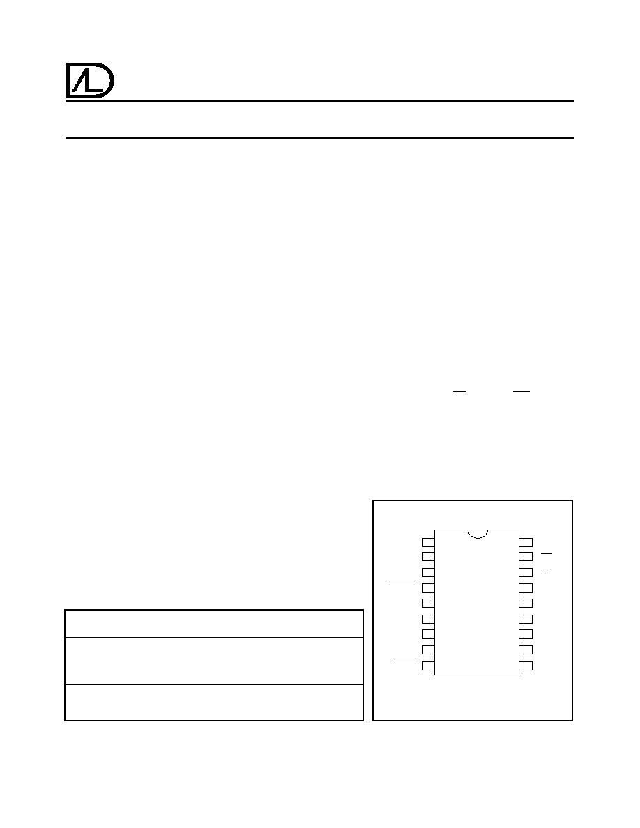
PIN CONFIGURATION
*
Note: N/C - No Conncection
1
2
3
14
15
16
4
13
5
12
DGND
A
6
7
8
10
11
S
2
PWRUP
XTAL
OUT
9
B
DV
PD, SD PACKAGE
17
18
S
3
C
OUT
V+
XTAL
IN
C
OUT
D
OUT
S
1
N/C
ALD521D
S
CLK
C
S
CS

ALD512D
Advanced Linear Devices
2
GENERAL DESCRIPTION (cont'd)
The ALD521D implements all the four phases of the ALD500
or ALD500R, namely auto zero, integrate, deintegrate, and
integrator zero phases. It also provides direct logic interface
to CMOS logic families. The ALD521D operates from an
external clock or its internal oscillator circuit along with an
external crystal. The internal system clock of the ALD521D
runs at a divide by 4 rate of the crystal or external clock
frequency.
A Data Valid (DV) low output during the auto zero phase
indicates when a 24 bit data word is available for output while
during the other phases DV remains in logical 1 state.
The ALD521D has control input pins for power down
(PWRUP), Chip Select (CS) and Integration time selection
(S1, S2 and S3). These pins can all be interfaced directly to
any 5V CMOS logic or microcontroller. They can also be
connected to a PC parallel printer port directly. When not
used, or if no programming control is desired, these pins can
be wired directly to their respective desired logic state, either
V+ or DGND (Ground).
Upon power on, the ALD521D initiates a power-on initializa-
tion cycle and resets all internal counters and registers. Then
it check the status of the PWRUPpin. A logical 0 on PWRUP
power up the ALD521D and a logical 1 on PWRUP power
down the ALD521D. If the ALD521D detects a logical 1 state
on the PWRUP pin, it in turn powers down the ALD500R to
save power during non-active period. At the same time, the
crystal oscillator circuit of the ALD521D is also stopped to
conserve power consumption. In power down mode the
current consumption of the ALD521D and the ALD500R is
less than 28
µ
A. To start and power up the ALD521D again,
simply put a logical 0 on PWRUP. An external microcontroller
can therefore use this pin to control the ALD521D power-on
SELECTING INTEGRATION TIME
For maximum 50/60 cycle line power noise rejection, Inte-
gration time t
INT
must be picked as a multiple of the period of
line power frequency. For example, t
INT
times of 16.667
msec, 33.333 msec, 66.667 msec, 100 msec, 200 msec and
300 msec maximize 60 Hz line power noise rejection; and 20
msec, 50 msec, 100 msec, 200 msec and 300 msec
maximize 50 Hz line power noise rejection. In general, the
longer the integration time , the better the noise rejection of
the line power noise, but it also takes longer to complete a
conversion cycle. A default recommended integration time of
100 msec offer the best tradeoff between noise perfor-
mance, conversion time and 50/60 cycle line power noise
rejection. The 100 msec integration time also offers the
benefit of being universally optimal for both 50 cycle line
power noise rejection and 60 cycle line power noise
rejection.
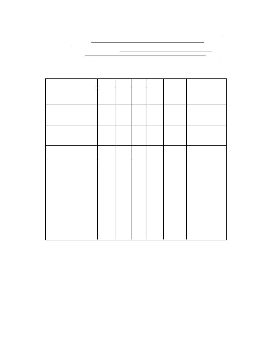
SELECTIONS S1
S2
S3
INTEGRATION TIME
APPROXIMATE
NUMBER OF
PINS
[18]
[1]
[2]
CONVERSION/SECOND
AC CYCLES
0
0
0
16.667ms
15
1
0
0
1
33.333ms
8
2
0
1
0
50.000ms
5
3
0
1
1
66.667ms
4
4
1
0
0
100.000 ms
3
6
1
0
1
166.667 ms
2
10
1
1
0
200.000 ms
1
12
1
1
1
300.000 ms
1
18
ALD521D PIN CONFIGURATION FOR DIFFERENT INTEGRATION TIMES
Note:"0" = GND; "1" = V+
status. If power down feature is not used, then the PWRUP
pin must be grounded to leave the ALD521D in continuously
power-on mode.
Chip Select (CS) enable selection of the ALD521D controller
when this pin is at logical 0 (CS Input = GND). When not
selected, when the CS pin is at logical 1, the ALD521D places
the DV, D
OUT
and S
CLK
pins in high impedance mode.
Multiple ALD521D devices can have these three pins wired
in parallel to a same external controller. When data is
required from a specific ALD521D, it is selected by having
its CS pin set at logical 0 state. The external controller can
send CS to only one ALD521D during each conversion cycle.
The CS must be valid for the duration of at least one complete
conversion cycle in order for the measurement data to be
valid. From an external controller, CS can be generated by
a latched output pin.
ALD512D
Advanced Linear Devices
3
ABSOLUTE MAXIMUM RATINGS
Supply voltage, V
+
+7.0V
Differential input voltage range
-0.3V to V
+
+0.3V
Power dissipation
600 mW
Operating temperature range
PD, SD package
0
∞
C to +70
∞
C
Storage temperature range
-65
∞
C to +150
∞
C
Lead temperature, 10 seconds
+260
∞
C
OPERATING ELECTRICAL CHARACTERISTICS
T
A
= 25
o
C
V+
= +5V unless otherwise specified
Parameter
Symbol
Min
Typ
Max
Unit
Test Conditions
Supply
Operating Voltage Range
V+
3
5
5.5
V
Supply Current
I
DD
4.0
6.8
mA
Input Characteristics
Low Input Voltage
V
IL
-0.3
1.0
V
High Input Voltage
V
IH
3.5
5.3
V
Input Leakage Current
I
IL
-10
10
µ
A
Output Characteristics
Low Output Voltage
V
OL
0.2
0.8
V
High Output Voltage
V
OH
3.6
4.8
V
C
L
= 10pF. Rise/Fall Times
t
R ,
t
F
25
125
nsec
Oscillator (OSC
IN,
OSC
OUT)
Crystal Frequency
f
XTL
3.6864
4.0
MHz
External Frequency (OSC
IN)
f
OSC
4.0
MHz
Timing Characteristics
Power Up Delay Time
t
PU
36
msec
Chip Select Setup Time
1
t
CS
1.1
µ
sec
Chip Select Delay Time
1
t
CD
1
Conv. Cycle
Data Valid Setup Time
t
DV
18
µ
sec
Data Valid Time Out Time
t
TO
5.5
msec
Data Out Time
t
DOUT
500
nsec
Serial Clock Low Time
t
SC
11
25
µ
sec
Data Not Valid Time
t
DNV
15
µ
sec
Integration Time
2
t
INT
16.666
300
msec
Integrator ZERO Time
t
INTZ
2
msec
Autozero Time
t
AZ
t
INT
msec
1
Chip Select Delay time (t
CD
) may be as short as 7
µ
sec, if start of auto zero phase cycle time could be
determined. For asynchoronous operation, t
CD
must be for a minimum of one complete conversion cycle to
assure synchronization to start of auto zero phase cycle time.
2
These are typical practical limits for Integration time. Lower Integration time than the minimum allows more
conversion cycles per second at reduced count resolution. Higher Integration time increases count
resolution, but requires increased capacitor value and lowered number of conversion cycles per second.
Deintegration time depends on selection of full scale input range, integration capacitor value and voltage
reference.
3
ESD Sensitive Device. Stresses above those listed under Absolute Maximum Ratings may cause permanent
damage to device and may affect device reliability.

ALD512D
Advanced Linear Devices
4
SERIAL DATA TRANSFER
The ALD521D has an internal 23 bit binary counter that can
be clocked out serially at the end of an analog conversion
cycle, or conversion, in an asynchronous handshake mode
with an external processor. The ALD521D also determines
the sign bit for the ALD500R where a logic 1 is a positive sign
and a logic 0 is a negative sign. This sign bit is the 24th bit
being sent out by the ALD521D.
At the end ofeach conversion, the ALD521D transmits a 24
bit serial word which requires an external processor to send
in 24 serial clock pulses. This 24 bit serial word consists of
content from the 23 bit binary counter with MSB as the first bit,
LSB the 23rd bit, followed by a sign bit as the last bit. A
transition of DV from a high to low state signals a completed
conversion and readiness for the start of the serial data
transfer.
During a conversion, the ALD521D maintains DV in a high or
logic 1 state. When it completes a conversion, the ALD521D
sets the DV to low. Simultaneously, the ALD521D puts the first
bit of the 24 bit binary word (MSB bit) on Dout. For this first
serial bit out, an external processor has a maximum of 5.5
msec to read the data on Dout and send a serial clock pulse
back to the ALD521D. This serial clock consists of a high to
low transition followed by a low to high transistion on S
CLK
.
When the ALD521D receives an external serial clock on S
CLK
,
it resets the DV to a high logic 1 state. In addition, it internally
clocks the next serial bit onto Dout and sets the DV to a low
state again.
Similarly, the ALD521D asynchronously transfers the
remainder of the 24 bit serial word to the external processor.
When all 24 serial bits have been clocked out, the ALD521D
resets the DV to a high state, and starts the integration phase
of the conversion. It keeps DV high for the remainder four
phases of the conversion cycle.
For an external processor to interface to the ALD521D, it
needs a minimum of 2 input pins and one output pin dedicated
for the task. The ALD521D has DV (data valid), and Dout (data
out) as outputs and S
CLK
(serial input clock) as input. The
external processor can use either an interrupt or data input for
the interface to DV. After the ALD521D sends the first DV high
to low transition, it waits for a maximum of 5.5 milliseconds for
an external serial clock at the S
CLK
input. If an external serial
clock is not received during that time, the ALD521D times out
internally, sets the DV to a high state, and starts a new
conversion. For example, if a conversion cycle is equal to 200
msec., DV will not be valid until 200 msec. later. The external
processor can read DV as an interrupt to begin clocking the 24
bit data. The external processor can also sample DV as a data
input or it can synchronize to the A and B outputs of the
ALD521D to determine when the next serial word becomes
available.
INTERFACE TO ALD500R
The ALD521D has A and B outputs that control the four
conversion phases of the ALD500/ALD500R and has Cout as
an input from the ALD500/ALD500R. Note that Cout of the
ALD500/ALD500R must be connected to pin 3 and pin 8 of the
ALD521D.
ALD512D
Advanced Linear Devices
5
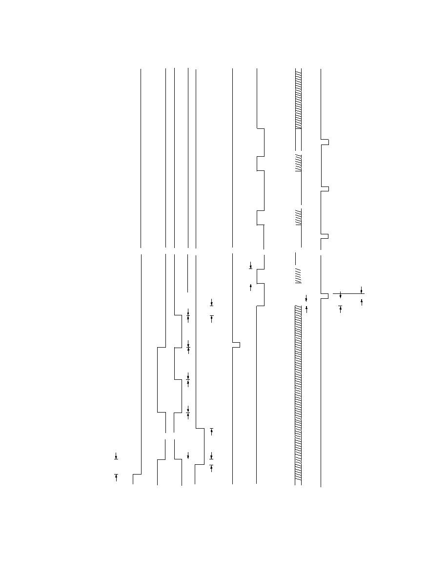
ALD521D TIMING DIAGRAM
PWRUP
A
B
CS
DV
t
INT
t
AZ
t
DINT
t
INTZ
t
AZ
t
CD
t
DV
t
CS
t
PU
SCLK
X
~
~
D
OUT
C
OUT
X
X
X
~
~
~
~
ALD521D
TIMING DIA
GRAM (Not to Scale)
~
~ ~
~
~
~ ~~ ~~ ~~
Data Not Valid
LSB
Bit 0
Polarity
Bit
MSB
Bit 22
t
D
OUT
t
DNV
t
SC
t
TO
~
~
~
~
ALD512D
Advanced Linear Devices
6
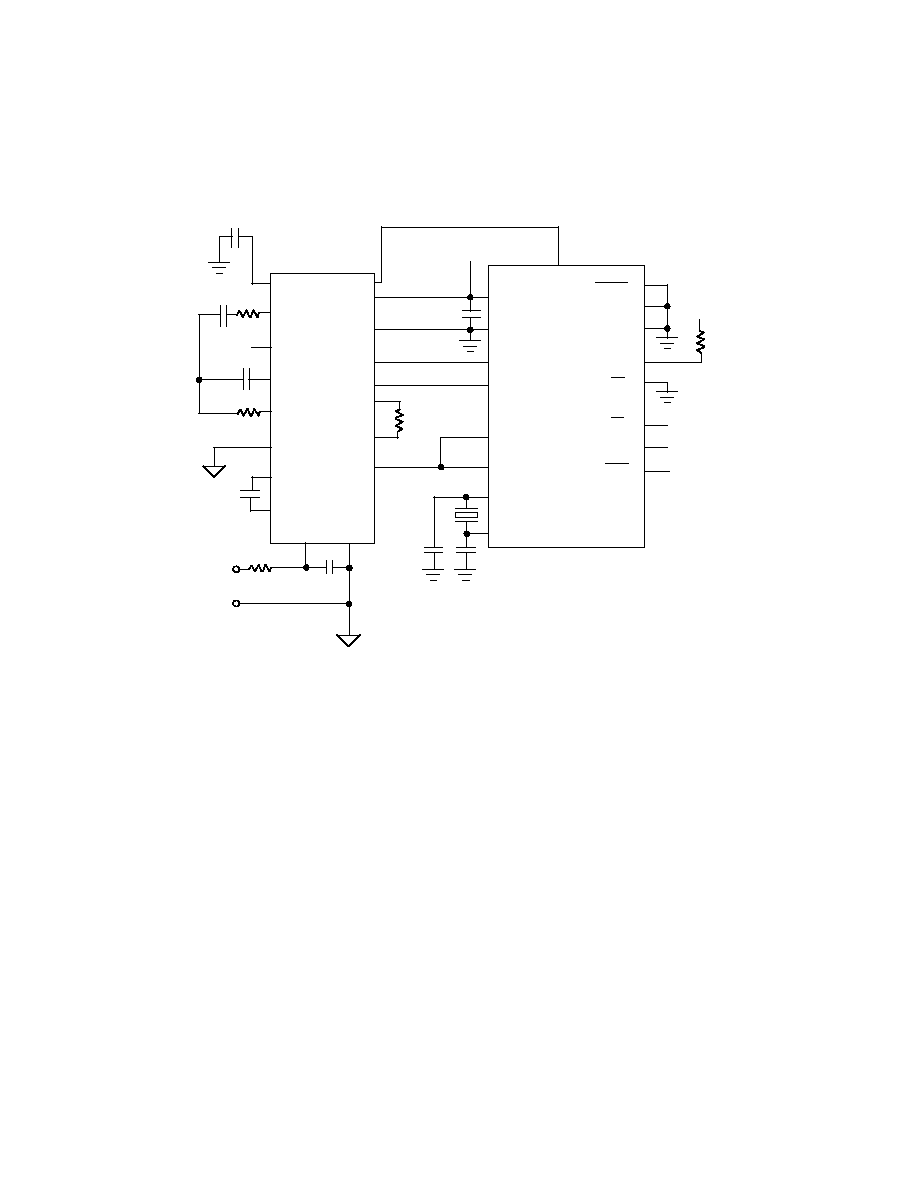
47pF
47pF
14 DGND
100k
v+
0.1uf
15uf
0.66uf
0.33uf
100k
0.33uf
V
IN
COM
9
17
8
13
10
Cout
PWRUP
Cout
DV
CS
DOUT
SCLK
100K
CINT
V-
CAZ
BUF.
AGND
C+REF
C-REF
0.1uf
14
13
20
19
16
15
12
11
6
7
Cs
V+
V+REF
V-REF
V+IN
V-IN
51k
3.6864 MHZ
1
2
3
4
5
6
7
8
S3
S2
S1
ALD500R
IB
A
B
DGND 18
Cs
15
16
17
18
1
3
4
2
ALD521D
XTAL OUT
XTAL IN
Cout
N/C
5 V+
12
11
A
B
Rint
Rref
C
Rin
v- =
2
V+
- 5V
= 5V
int
ANALOG INPUT
DIGITAL OUTPUTS
ALD521D TYPICAL APPLICATION