 | –≠–ª–µ–∫—Ç—Ä–æ–Ω–Ω—ã–π –∫–æ–º–ø–æ–Ω–µ–Ω—Ç: ALD523DSH | –°–∫–∞—á–∞—Ç—å:  PDF PDF  ZIP ZIP |
©
©
©
©
2001 Advanced Linear Devices, Inc., 415 Tasman Drive, Sunnyvale, California 94089-1706, Tel: (408) 747-1155, Fax: (408) 747-1286
ALD523D
12/01
http://
www.aldinc.com
1 of 20
ALD523D
MULTIFUNCTION 7-DIGIT SERIAL INPUT DISPLAY MODULE CONTROLLER
PRODUCT FEATURES AND BENEFITS
Up to 7 full digit plus sign (
±
9999999) display
Built-in 21 bit serial binary to
± 6Ω
digit decimal converter
Compatible with industry standard 1-line x 16 and
2-line x 16 Character Display Modules
User defined 16-alphanumeric character TITLE field
and up to three 8-alphanumeric character UNIT fields
Wide range of alphanumeric display characters
Functional with either LCD or VFD display modules
with column drivers
Designed to operate optionally with ALD500/ALD500R
Precision Analog Signal Processors or directly with serial
inputs
User selected integration time and conversion speed
Cost effective and multipurpose stand alone operation
3 optional modes of operation:
- Mode A, calibrated reference mode
- Mode B, ratiometric mode
- Mode C, display only mode
Support external serial binary input (up to 32 bits)
3-wire serial interface to microprocessors or
microcontrollers
Electrical programmable memory interface
Crystal oscillator frequency up to 8 MHz
Single 3V to 5V power supply
Up to 3 separate sets of 7-DIGIT Display Sets
3 sets of user defined 64-bit arithmetic multiplication factor
Software programmable serial data bit mask and sign
polarity mask
3 different sets of user selected data sample averaging with
up to maximum of 128X sampling
Optional 13-function user configurable hardware selection
switches
Automatic zero level shifting during power-on-reset
Automatic zero level overwrite feature
Adjustable decimal point placement with trailing digit
blanking
External 1K EEPROM memory for easy change of factory
settings
Sleep mode with Auto Power-On-Reset.
Easy setup of calibration and system setup parameters
No software programming required
PC Interface Software provided for Calibration and Setup
modes
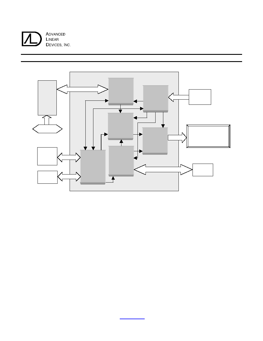
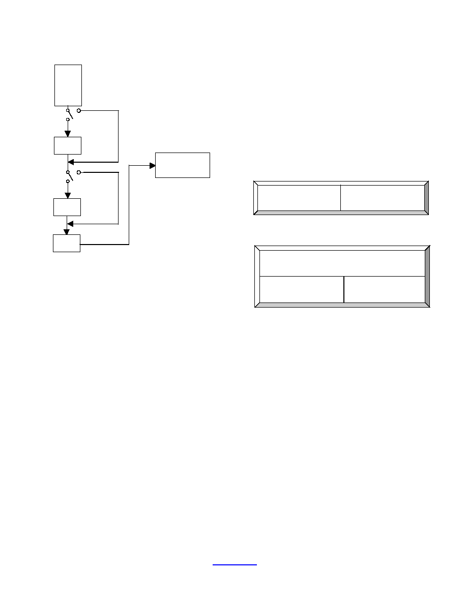
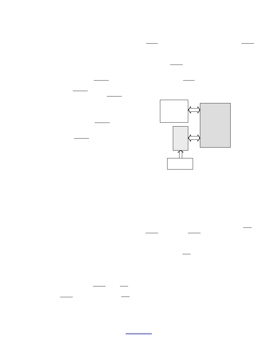
EEPROM
MEMORY
CONTROLLER
DUAL SLOPE
A/D 4-PHASE
CONTROLLER
SERIAL
BINARY TO
6Ω
-DIGIT
DECIMAL
CONVERTER
DISPLAY
MODULE
CONTROLLER
SERIAL I/O
INTERFACE
LOGIC
CONTROL
LOGIC
CHARACTER
DISPLAY MODULE
FUNCTIONS
SELECTORS
EEPROM
ALD523D BLOCK DIAGRAM
ALD500
ANALOG
INPUT
EXTERNAL
SERIAL
BINARY
INPUT
PC
©
©
©
©
2001 Advanced Linear Devices, Inc., 415 Tasman Drive, Sunnyvale, California 94089-1706, Tel: (408) 747-1155, Fax: (408) 747-1286
ALD523D
12/01
http://
www.aldinc.com
2 of 20
PRODUCT APPLICATIONS
Embedded (up to ± 6Ω -digit) digital panel meter
Customized/specialized instrument display
High precision DC voltage meters
Dedicated precision monitors
High resolution A/D converter with display
High accuracy and low noise weigh scale systems
Multifunction precision measurement instruments
Serial binary input to decimal/character display converter
Portable battery operated display systems
.
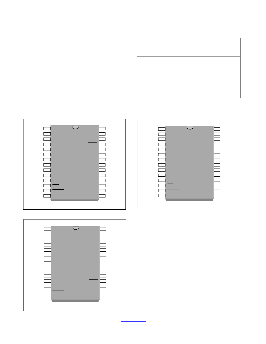
ALD523D PIN CONFIGURATIONS
PRODUCT ORDERING INFORMATION
OPERATING TEMPERATURE RANGE
*
0
o
C to +70
o
C
0
o
C to +70
o
C
28-Pin Plastic DIP Package
(PDIP)
28-Pin Small Outline Package
(SOIC)
ALD523DPH
ALD523DSH
*: Contact factory for industrial temperature range
CALIBRATED REFERENCE (MODE-A)
ALD523D
1
2
3
4
5
6
7
8
9
10
11
12
13
14
15
16
17
18
19
20
21
22
23
24
25
26
27
28
S1/SCL
DSA1/D6
DSA2/D7
PWRCS
SDA
B1/D4
B2/D5
V
+
XTAL2
XTAL1
DVCS
CAL
CS
B
WP
A
COUT
COUT
SEL0/D0
SEL1/D1
DEC1/D2
DGND
DATIN
SCLK
DATOUT
S2/EN
S3/RS
DEC2/D3
PH, SH PACKAGE
RATIOMETRIC (MODE-B)
1
2
3
4
5
6
7
8
9
10
11
12
13
14
15
16
17
18
19
20
21
22
23
24
25
26
27
28
ALD523D
S1/SCL
DSA1/D6
DSA2/D7
PWRCS
SDA
B1/D4
B2/D5
V
+
XTAL2
XTAL1
DVCS
CAL
CS
B
WP
A
COUT
COUT
SEL0/D0
SEL1/D1
M/D2
DGND
DATIN
SCLK
DATOUT
S2/EN
S3/RS
Z/D3
PH, SH PACKAGE
DISPLAY ONLY (MODE-C)
1
2
3
4
5
6
7
8
9
10
11
12
13
14
15
16
17
18
19
20
21
22
23
24
25
26
27
28
ALD523D
SCL
DSA1/D6
DSA2/D7
PWRCS
SDA
B1/D4
B2/D5
V
+
XTAL2
XTAL1
DVCS
CAL
N/C
N/C
WP
N/C
N/C
N/C
SEL0/D0
SEL1/D1
DEC1/D2
DGND
DATIN
SCLK
DATOUT
EN
RS
DEC2/D3
PH, SH PACKAGE

©
©
©
©
2001 Advanced Linear Devices, Inc., 415 Tasman Drive, Sunnyvale, California 94089-1706, Tel: (408) 747-1155, Fax: (408) 747-1286
ALD523D
12/01
http://
www.aldinc.com
3 of 20
GENERAL DESCRIPTION
The ALD523D is a Multifunction 7-Digit Serial Input
Display Module Controller designed to interface directly
to ALD500 or ALD500R integrating dual slope precision
analog processors as a chip set for building a high
precision and high accuracy analog-to-digital converter
system with auto zero and auto-polarity. The ALD523D
also functions as an universal serial input 7-digit display
module controller that interfaces to most popular industry
standard serial data formats from other microprocessors or
data converters. It is designed for easy setting of industry
standard Character Display Modules (CDM) such as 1-line
by 16-character or 2-line by 16-character LCD or VFD
display modules. The ALD523D is an enhanced version of
the ALD521D digital controller. The ALD523D functions
in three separate operating modes, namely calibrated
reference (mode-A), ratiometric (mode-B), and display
only (mode-C).
The ALD523D digital controller operates as a master
display module controller in either a stand-alone mode or
in an external microprocessor control mode. In the external
microprocessor control mode, the ALD523D can directly
interface with a PC under PC software control via a
standard parallel printer port. This external control mode
is managed by the Serial I/O Interface Logic inside the
ALD523D.
In the stand-alone mode, the ALD523D makes continuous
measurements, and includes all the necessary functions to
fully control a CDM. In the stand-alone mode, ALD523D
operates in conjunction with a 1K EEPROM chip to
preserve the setup parameters and arithmetic (calibration)
parameters of the ALD523D.
The setup and arithmetic parameters are uploaded to the
EEPROM via ALD523D Setup and Calibration PC
software (DVM523). The ALD523D communicates to the
EEPROM on a handshake protocol governed by the
EEPROM Memory Controller inside the ALD523D.
The ALD500/ALD500R dual slope precision analog
processors consist of on-chip digital control circuitry to
accept control inputs, integrating buffer amplifiers, analog
switches, and voltage comparators. It functions in four
operating phases, namely auto zero, integrate, de-integrate,
and integrator zero phases. At the end of a conversion, the
comparator output goes from high to low when the
integrator crosses zero during de-integration.
ALD500/ALD500R dual slope precision analog
processors also provide direct logic interface to
ALD523D.
The ALD523D implements the logic and timing for all the
four phases of the ALD500/ALD500R, namely auto zero,
integrate, de-integrate, and integrator zero phases in mode-
A and mode-B operations. These four phases are
governed by the Dual Slope A/D 4-Phase Controller inside
the ALD523D. The ALD523D operates from an external
clock or its internal oscillator circuit along with an external
crystal. The internal system clock of the ALD523D runs
at a frequency which can be selected at divide-by N (4, 8,
or 64) rate of the crystal (or external) clock frequency.
The ALD523D offers up to 3 display settings, known as
display sets, namely "DGS1", "DGS2" and "DGS3".
"DGS1" also has an optional hardware decimal point
setting mode, known as "DGS0", which allows the user to
use hardware jumper switches to set decimal point
position. Each display set allows a full 7-digit decimal
number to be converted from a 16-bit to 32-bit serial
binary number using the Serial Binary To 6Ω-Digit
Decimal Converter inside the ALD523D. This 6Ω-digit
decimal number can also be scaled by a MULTIPLIER
number, and the result of the scaled number displayed on
the CDM through the Display Module Controller within
the ALD523D. Additional display parameters that can be
manipulated are: Digit Blanking, which allows user
selection of number of digits to display; Decimal Point
placement, which controls placement of decimal point, if
any. Up to 3 sets of display UNIT fields are available,
each with a combination of alphanumeric characters up to
8 characters long.
The ALD523D also features hardware control-input pins
for power down (PWRCS), integration time selection (S1,
S2 and S3), data sample averaging (DSA1 and DSA2),
digit blanking (B1 and B2), decimal point placement
(DEC1 and DEC2), zero offset (M and Z), and display set
selection (SEL0 and SEL1). When not used, or if no
control is desired, each of these optional pins are wired to
their respective desired logic state, either V
+
or Ground
(DGND), through pull-up or pull-down resistors. The
functions of the control-input pins are managed by the
Control Logic section in the ALD523D.
MODES OF OPERATIONS
The ALD523D functions in either single operating mode
or multiple operating modes, namely calibrated reference
(mode-A), ratiometric (mode-B), and display only (mode-
C). In the single operating mode, ALD523D operates in
one of the three modes of operation, either mode-A, mode-
B or mode-C. In the multiple operating modes, the
ALD523D can operate interchangeably in each of the three
©
©
©
©
2001 Advanced Linear Devices, Inc., 415 Tasman Drive, Sunnyvale, California 94089-1706, Tel: (408) 747-1155, Fax: (408) 747-1286
ALD523D
12/01
http://
www.aldinc.com
4 of 20
different operating modes. This feature becomes useful
for applications that require multiple modes of operations
where up to three different types of measurements are
made and displayed.
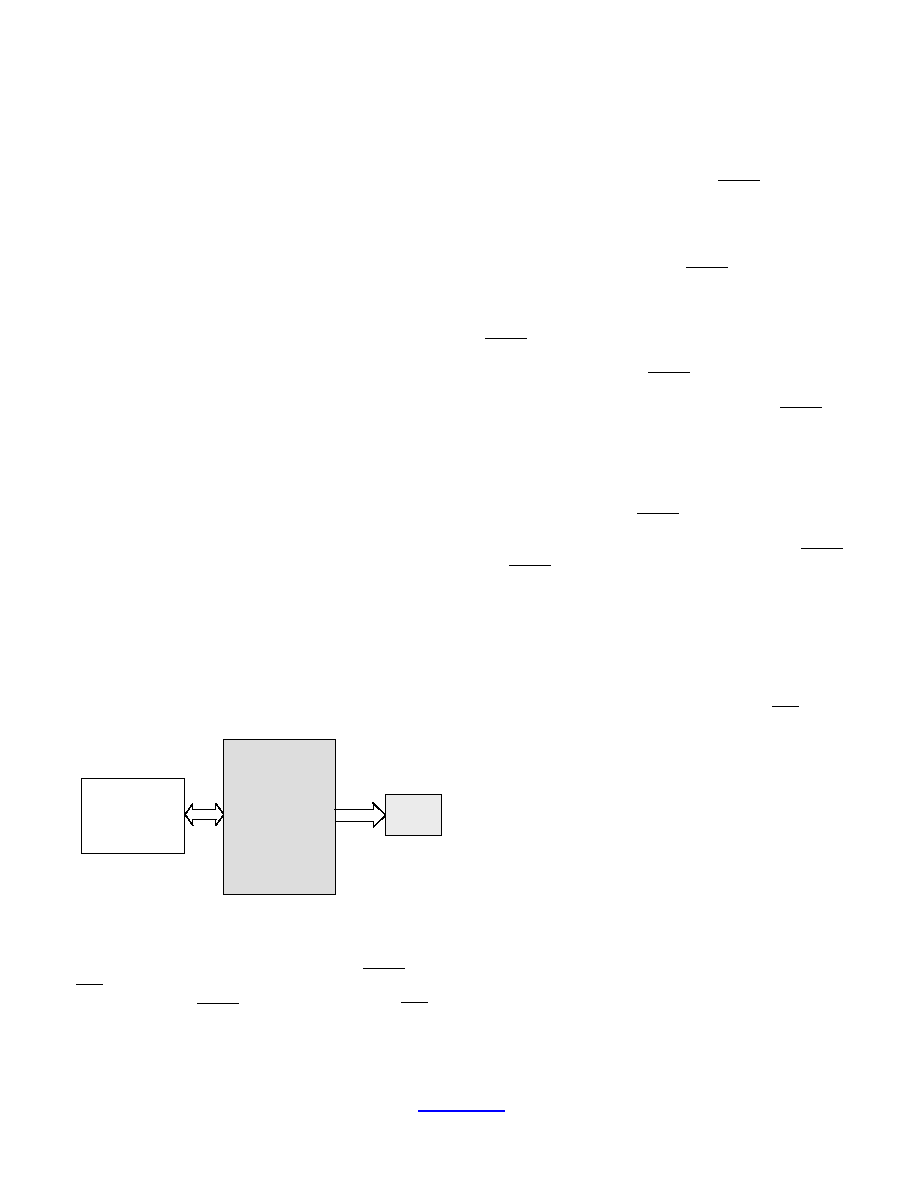
I.
CALIBRATED REFERENCE MODE (MODE-A)
The calibrated reference mode (mode-A) is primarily
intended for measurements against a calibrated reference
voltage. The reference voltage can either be internal or
external. In this mode, the ALD523D runs its internal
analog-to-digital controller to manage data conversion
from an analog-to-digital converter chip with calibrated
reference voltage such as the integrating dual slope
precision analog processors ALD500R. One of the
practical applications of utilizing this mode of operation is
a precision digital voltmeter system design (see the
Application Design Note-AN523DA).
In this mode, ALD500 can also be used instead of the
ALD500R, with an external voltage reference. The block
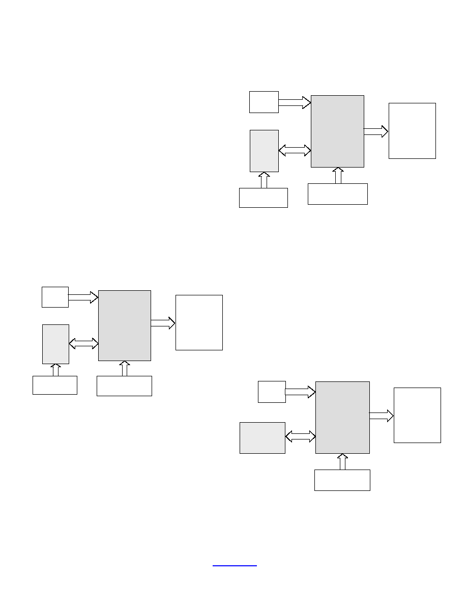
diagram of mode-A is shown in figure 1. See ALD523D
pin configuration and identification section for mode-A
pin layout and description.
Figure 1. Calibrated reference mode (mode-A) block
diagram.
II.
RATIOMETRIC MODE (MODE-B)
The ratiometric mode (mode-B) is primarily intended for
measurements against a ratiometric reference voltage. In
this mode, the ALD523D runs its internal analog-to-digital
controller to manage data conversion from an analog-to-
digital converter chip such as the integrating dual slope
precision analog processors ALD500 with ratiometric
reference voltage. One of the practical example
applications of utilizing this mode of operation is a
precision weigh scale system design (see the Application
Design Note-AN523DB). The block diagram of mode-B
is shown in figure 2. See ALD523D pin configuration and
identification section for mode-B pin layout and
description.
Figure 2. Ratiometric mode (mode-B) block diagram.
III.
DISPLAY ONLY MODE (MODE-C)
The display only mode (mode-C) is primarily intended for
receiving a ready external serial binary data, converting
and processing the data, and showing the processed data
on the CDM. In this mode, the ALD523D runs its internal
display controller to manage, process, and display the
received serial binary data from a transmitting instrument
or device. One of the applications of utilizing this mode of
operation is an external interface to ALD MB1S precision
digital voltmeter system. The block diagram of mode-C is
shown in figure 3. See ALD523D pin configuration and
identification section for mode-C pin layout and
description.
Figure 3. Display only mode (mode-C) block diagram.
ALD523D
CHARACTER
DISPLAY
MODULE
(1-LINE)
OR
(2-LINES)
FUNCTIONS
SELECTORS
ALD500R
ANALOG
INPUT
1K
EEPROM
ALD523D
FUNCTIONS
SELECTORS
ALD500
ANALOG
INPUT
1K
EEPROM
CHARACTER
DISPLAY
MODULE
(1-LINE)
OR
(2-LINES)
ALD523D
FUNCTIONS
SELECTORS
EXTERNAL
INSTRUMENT
(SERIAL DATA)
1K
EEPROM
CHARACTER
DISPLAY
MODULE
(1-LINE)
OR
(2-LINES)

©
©
©
©
2001 Advanced Linear Devices, Inc., 415 Tasman Drive, Sunnyvale, California 94089-1706, Tel: (408) 747-1155, Fax: (408) 747-1286
ALD523D
12/01
http://
www.aldinc.com
5 of 20
ALD523 SETUP AND CALIBRATION SOFTWARE
In the stand-alone mode, ALD523D operates in
conjunction with a 1K EEPROM chip to preserve the
setup and arithmetic (calibration) parameters of the
ALD523D. These parameters are utilized to fully control
the CDM and measurement functions. The parameters are
preset by the user through the ALD523D Setup and
Calibration PC software known as DVM523.EXE, and
later uploaded to the EEPROM via a standard parallel
printer port. See the ALD523D Setup and Calibration
User Guide (DVM523) for more details.
SELECTING AND CONFIGURING MODES OF
OPERATIONS
The three ALD523D modes of operations, namely mode-
A, mode-B, and mode-C are configured in the .CDS file
(see Table 1 of the ALD523D Setup and Calibration
Software User Guide), and are selected by means of user
selection of SEL0 and SEL1 control inputs of the
ALD523D. Each display set "DGSx" has an associated
mode parameter "Mx" which specifies the mode of
operation. Hence, "DGS1", "DGS2", and "DGS3" have 3
associated mode specifying parameters "M1", "M2", and
"M3", respectively. Each "Mx" parameter can be preset to
either "Mode-A", "Mode-B", or "Mode-C".
I.
CALIBRATED REFERENCE MODE (MODE-A)
Mode-A can be selected by setting the nibble "M1"
parameter, or "M2" or "M3" of the byte "M2-M3"
parameter to an "A" (HEX) in the .CDS file. "M1", "M2",
and "M3" are the mode selection parameters associated
with "DGS1", "DGS2", and "DGS3" display sets,
respectively.
In mode-A or mode-B operation, the bit masking
"SMSK1" to "SMSK4" and the polarity bit masking
"SMSK5" to "SMSK8" parameters are not utilized.
However, this mode transmits a 24-bit serial word on pin
26, DATOUT. This 24-bit serial word consists of 23-bit
binary data with MSB as the first bit, LSB the 23
rd
bit,
followed by a sign bit as the last bit. The sign bit is a
logical "1" as a positive sign, and logical "0" as a negative
sign.
II.
RATIOMETRIC MODE (MODE-B)
Mode-B can be selected by setting the nibble "M1"
parameter, or "M2" or "M3" of the byte "M2-M3"
parameter to an "B" (HEX) in the .CDS file.
When the ALD523D is powered up the first time or after
power-on-reset, a zero correction is automatically set by
zeroing out the reading. This automatic zero correction
feature can be manually overwritten by the Z switch (see
Table 5) at any time. The overwrite feature is embedded
to eliminate the long wait time at long integration time,
and add flexibility to perform zero correction at any time.
However, the faster the integration time set, the less the
wait time is needed to perform the automatic zero
correction (i.e. it takes typically from about 1 to 14
seconds to automatically zero out a reading for integration
time of 16.66 ms to 300 ms, respectively).
III.
DISPLAY ONLY MODE (MODE-C)
Mode-C can be selected by setting the nibble "M1"
parameter, or "M2" or "M3" of the byte "M2-M3"
parameter to an "C" (HEX) in the .CDS file. In mode-C
operation, switches "S1", "S2", and "S3" are internally
disabled.
In mode-C operation, the ALD523D receives a maximum
serial word length of 32 bits in accordance to 32 serial
clock pulses, and processes a maximum of 21-bit serial
word plus 1 sign bit within this 32-bit serial word. This
21-bit serial word can be any 21-bit consecutive serial data
stream segment within the 32-bit serial clocks, as selected
by programming of the bit masks "SMSK1" through
"SMSK4". The length of the received serial word is
governed by a DVCS signal. A transition of DVCS from
high to low state signals the start of the serial input data bit
stream clocking. A transition of DVCS from low to high
state stops the serial input data bit stream clocking.
After an external instrument or processor sets the DVCS to
logic 0, the DATIN terminal of the ALD523D is ready for
serial input data stream. The ALD523D reads the first bit
of the serial input data stream on DATIN and sends a
serial clock pulse on the SCLK as an acknowledge signal
to the external instrument or processor. Then the
ALD523D reads the second bit of the serial input data
stream and sends out a second SCLK clock pulse. This
serial data reading and clocking process continues until
DVCS is set to high state or until a maximum of 32 serial
input data bits have been read. The serial clock SCLK
consists of a low to high transition followed by a high to
low transition.
The maximum converted decimal number from this 21-bit
binary data plus sign bit is
± 9999999, when a suitable
multiplier and an appropriate conversion factor are used.
The sign bit is defined as logic "0" as a positive sign, and
logic "1" as a negative sign. Alternatively, the sign bit
©
©
©
©
2001 Advanced Linear Devices, Inc., 415 Tasman Drive, Sunnyvale, California 94089-1706, Tel: (408) 747-1155, Fax: (408) 747-1286
ALD523D
12/01
http://
www.aldinc.com
6 of 20
polarity and the serial clock SCLK polarity can be
inverted, as described in the next section.
The positions of the serial data bits and sign bit within a
given serial data word are determined by the 32 bit data bit
mask register "SMSK1" to "SMSK4" and the 32 bit sign
bit mask register "SMSK5" to "SMSK8" parameters in the
.CDS file. Bit masking rules are as follows:
1. Maximum serial word length that the ALD523D can
receive are 32 bits in 32 SCLK clock cycles. One of
the serial bits can be optionally a sign bit. If a serial
word has less than 32 bits, the last clock of the SCLK
clock stream when DVCS goes from a "0" to a "1"
stops the data word counter.
2. Maximum serial data bits that the ALD523D can
process are 21 bits plus 1 sign bit for a total of 22 bits.
3. Minimum serial data bits that the ALD523D can
process are 2 bits, including a sign bit. The number of
clock cycles between when DVCS goes from "1" to
"0" to when DVCS goes from "0" to "1" defines the
total input serial word length, right justified, from bit
0 of the 32 bit input mask register.
4. The input serial data bits must be in a consecutive
order, from MSB bit first to LSB bit last.
5. The sign bit can be anywhere outside the serial data
bits stream but within the serial data word.
BIT AND SIGN MASKING
Bit masking is set by the user by programming SMSK1
through SMSK4 from memory address 60H to 63H.
SMSK1 indicates the position of the first 8 bits of a 32-bit
serial data word mask. SMSK2, SMSK3 and SMSK4
indicates the position of the next 24 bits of the 32-bit serial
data word mask, respectively. Initially, all 32 bits are set
to 0. When the last "1" bit is set anywhere within the 32
bit serial data word, it sets the LSB bit position. The "1"
bit starts at MSB, followed by "1" bits, until the LSB bit
is reached. After the LSB bit, any subsequent bit must be
left as "0" bits. The number of "1" bits between MSB bit
and the LSB bit determines the length of the serial data
word.
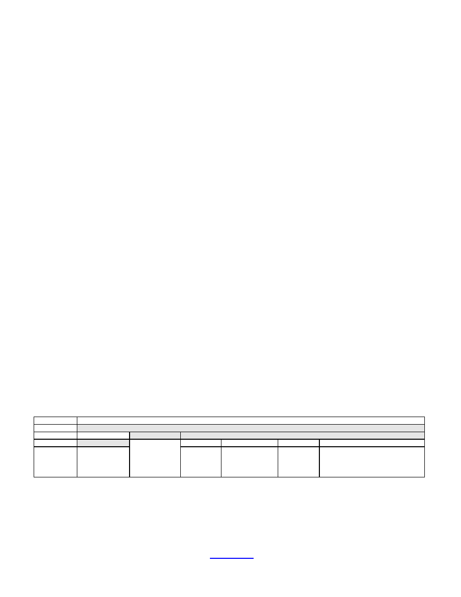
SMSK1
SMSK2
SMSK3
SMSK4
Byte-1
Byte-2
Byte-3
Byte-4
Binary
00000000
00001111
11111111
11110000
Hexadecimal
00
0F
FF
F0
bit31
bit0
Table 1. Serial data bit masking technique
.
Table 1 illustrates an example of the serial bit masking
technique. In this example, there are 23 SCLK clock
cycles, a sign bit and a 16 bit data word. SCLK clock starts
at bit 7 of SMSK2. MSB starts on the 4
th
clock cycle, or
bit 4 of SMSK2, of the serial data stream. Data is being
continuously clocked into the ALD523D until the 23
rd
clock cycle or until DVCS goes from "0" to "1". The LSB
of the data word is positioned at the 19
th
clock cycle. The
length of the serial word is determined by the number of
consecutive "1" in the masking bits, which is 16 bits.
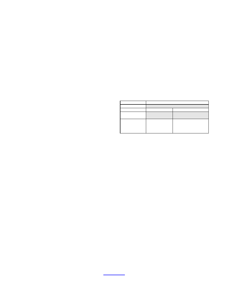
Sign masking is set by the user by programming SMSK5
through SMSK8 from memory address map 64H to 67H.
Initially, all 32 bits from SMSK5 to SMSK8 are set to 0.
A "1" bit anywhere between SMSK5 through SMSK8
indicates the position where the sign information is
located. There can only be one "1" bit within the 32-bit
serial data stream, situated outside the serial data bit
stream, and all remaining bits must be "0" bits. In this
example, the data word has 23 clock cycles.
Table 2 illustrates the example of sign bit masking
technique. The sign bit data is available on the first clock
cycle of the 23-bit data word stream. In this example,
placing a "1" anywhere between the fourth bit of SMSK6,
through all the bits of SMSK7, until the fifth bit of
SMSK8, corresponding to between the 4
th
clock cycle to
the 19
th
SCLK clock cycle, is not allowed. This example
is also valid for any number of SCLK, between 23 and 32,
of the input data word, while DVCS is low.
SMSK5
SMSK6
SMSK7
SMSK8
Byte-5
Byte-6
Byte-7
Byte-8
Binary
00000000
01000000
00000000
00000000
Hexadecimal
00
40
00
00
bit31
bit0
Table 2. Sign bit masking technique
.
In default mode, the sign bit is defined by logic "0" as a
positive sign, and logic "1" as a negative sign, and the
serial clock is SCLK. As an option, the sign bit and the
serial clock polarity can be inverted by setting "Mx" equal
to "D" (HEX) instead of "C" (HEX). The serial clock now
becomes SCLK, and the sign bit polarity is defined as
logic "1" for a positive sign, and logic "0" for a negative
sign (see Table 1 of the ALD523D Setup and Calibration
Software User Guide).
SELECTING AND CONFIGURING DISPLAY LINE
WITH FREQUENCY MODE AND INPUT CLOCK
DIVIDER
The ALD523D is designed to be compatible with industry
standard 1-line x 16-character and 2-line x 16-character
CDM, and to operate under different input frequencies of
the clock source. This feature is programmable through
the "SETF" parameter in the .CDS file. The "SETF"
parameter is a 4-bit hexadecimal number (0-B) located on
the first line of the .CDS file, and corresponds to address
00H of the EEPROM.
©
©
©
©
2001 Advanced Linear Devices, Inc., 415 Tasman Drive, Sunnyvale, California 94089-1706, Tel: (408) 747-1155, Fax: (408) 747-1286
ALD523D
12/01
http://
www.aldinc.com
7 of 20
Figure 4. Programmable input frequency divider of the
clock source.
The 4-bit hexadecimal number defines the selection of
either 1-line x 16-character or 2-line x 16-character
display, along with the operating frequency modes (low or
high) and the input frequency dividers of 4, 8, and 64,
respectively. The low or high frequency mode operates
the ALD523D in the low emission mode or standard
mode, respectively. The input frequency divider further
scales down the input clock source from a divide by 4 by
any integer number of 1, 2, and 16 as illustrated in figure
4.
SELECTING AND CONFIGURING DISPLAY
TITLE LINE
With the ALD523D, one 16-character display TITLE line
field can be custom programmed according to user's
choices, and displayed on the first line of the 2-line by 16-
character CDM. The characters of this TITLE line field is
configured through "TTL1" to "TTL16" parameters,
which are 16-byte hexadecimal numbers located on the
second and third lines of the .CDS file, and corresponds to
addresses from 08H to 17H of the EEPROM memory
address map (see Table 3 character codes and patterns in
the ALD523D Setup and Calibration Software User
Guide). TITLE line field is not displayed when 1-line by
16-character display is used.
DATA & UNIT DISPLAY LINE
The first line of the 1-line x 16-character or the second line
of the 2-line x 16-character CDM is divided into a DATA
field and a UNIT field, as illustrated in figure 5. The
ALD523D converts a 24-bit plus sign bit serial data stream
to a 7-digit decimal number with +/- sign. The 7-digit
number, when displayed with +/- sign and a decimal point,
takes up a total of 9 characters. This 7-digit number is
displayed in the DATA field starting on the first character
of a 1-line CDM and starting on the first character of the
second line of a 2-line CDM.
Figure 5. Character Display Module TITLE, DATA, and
UNIT fields.
The remaining characters of the 16-character line of the
CDM are used as UNIT character displays. The user can
put any combination of characters in the remaining
character fields. In general, these characters are used as a
display of a UNIT of measure, such as "VOLT" or
"KILOGRAM" or "PSI".
A maximum of 8 characters can be displayed in the UNIT
field. However, if the first character of the UNIT field is a
"blank", or 20 (HEX), then a full 7 digit plus sign and
decimal point can be displayed. Otherwise, only a
maximum of 6 digit plus sign and decimal point are
displayed, as the last digit of the 7 digit number is over-
written by the UNIT display character.
For example, using "KILOGRAM" as a UNIT display,
maximum digits displayed are 6 digits. In order to have 7
digits displayed, the UNIT label may be changed to
"_KGM" where the first character of the 8-character UNIT
field is a blank character 20 (HEX).
SETF
SETF
X-TAL
OSC
Or
EXT.
CLOCK
˜
˜
˜
˜ 2
˜
˜
˜
˜ 16
˜
˜
˜
˜ 4
SYSTEM
CLOCK
1-LINE x 16-CHARACTER CDM
2-LINE x 16-CHARACTER CDM
TITLE LINE FIELD
DATA FIELD
UNIT FIELD
DATA FIELD
UNIT FIELD
©
©
©
©
2001 Advanced Linear Devices, Inc., 415 Tasman Drive, Sunnyvale, California 94089-1706, Tel: (408) 747-1155, Fax: (408) 747-1286
ALD523D
12/01
http://
www.aldinc.com
8 of 20
SELECTING AND CONFIGURING DISPLAY
SETTINGS
The ALD523D uses SEL0 and SEL1 control-input pins for
selecting different display sets "DGS0", "DGS1",
"DGS2", and "DGS3". Each display set "DGSx" has an
associated mode of operation "Mx", unit display "UNTx",
decimal point placement "LxDEC", and multiplier scale
factors "
±CALx", where x=0, 1, 2 or 3.
The SEL0 and SEL1 switches have 4 logical states of
operations as described in Table 3. Each logical state
combination selects different measurement labels/units,
scale factors, decimal point location, and mode selections.
In all modes of operation, the SEL0 and SEL1 software
switch setting selections override the hardware jumper
functions of the DEC1 and DEC2 or M and Z switches
when either SEL0 or SEL1 are set to logical "1".
When SEL0=0 and SEL1=0, the ALD523D selects
display set "DGS0", which consists of a combination of
"M1", "UNT1", "+CAL1" and "
-CAL1" parameters from
addresses 00H, 18H to 1FH, 30H to 37H, and 38H to 3FH
of the EEPROM memory, respectively. In the calibrated
reference mode (mode-A) and the display only mode
(mode-C), DEC1 and DEC2 hardware jumper switches are
used to place decimal point. In mode-B operation, no
decimal point is displayed.
When SEL0=1 and SEL1=0, the ALD523D selects
display set "DGS1", which consists of a combination of
"M1", "L1DEC", "UNT1", "+CAL1" and "
-CAL1"
parameters from addresses 00H, 05H, 18H to 1FH, 30H to
37H, and 38H to 3FH of the EEPROM memory,
respectively. The decimal point is placed according to the
content of the "L1DEC" parameter.
When SEL0=0 and SEL1=1, the ALD523D selects
display set "DGS2", which consists of a combination of
"M2", "L2DEC", "UNT2", "+CAL2" and "
-CAL2"
parameters from addresses 01H, 06H, 20H to 27H, 40H to
47H, and 48H to 4FH of the EEPROM memory,
respectively. The decimal point is placed according to the
content of the "L2DEC" parameter.
When SEL0=1 and SEL1=1, the ALD523D selects
display set "DGS3", which consists of a combination of
"M3", "L3DEC", "UNT3", "+CAL3" and "
-CAL3"
parameters from addresses 01H, 07H, 28H to 2FH, 50H to
57H, and 58H to 5FH of the EEPROM memory,
respectively. The decimal point is placed according to the
content of the "L3DEC" parameter.
Each of the "M1", "M2", and "M3" parameters is a 4-bit
hexadecimal number located on the first line of the .CDS
file (see Table 1 of the ALD523D Setup and Calibration
Software User Guide for the data sheet layout). Each of
these "M1", "M2", and "M3" parameters can have content
data of "A", "B", "C" or "D" which corresponds to mode-
A, mode-B, mode-C default mode, or mode-C clock and
sign bit inverted polarity mode, respectively.
Each of the "L1DEC", "L2DEC", and "L3DEC"
parameters is an 8-bit hexadecimal number at addresses
05H, 06H, and 07H of the first line location of the .CDS
file, respectively.
Table 3. Display setting switch configurations and operations
.
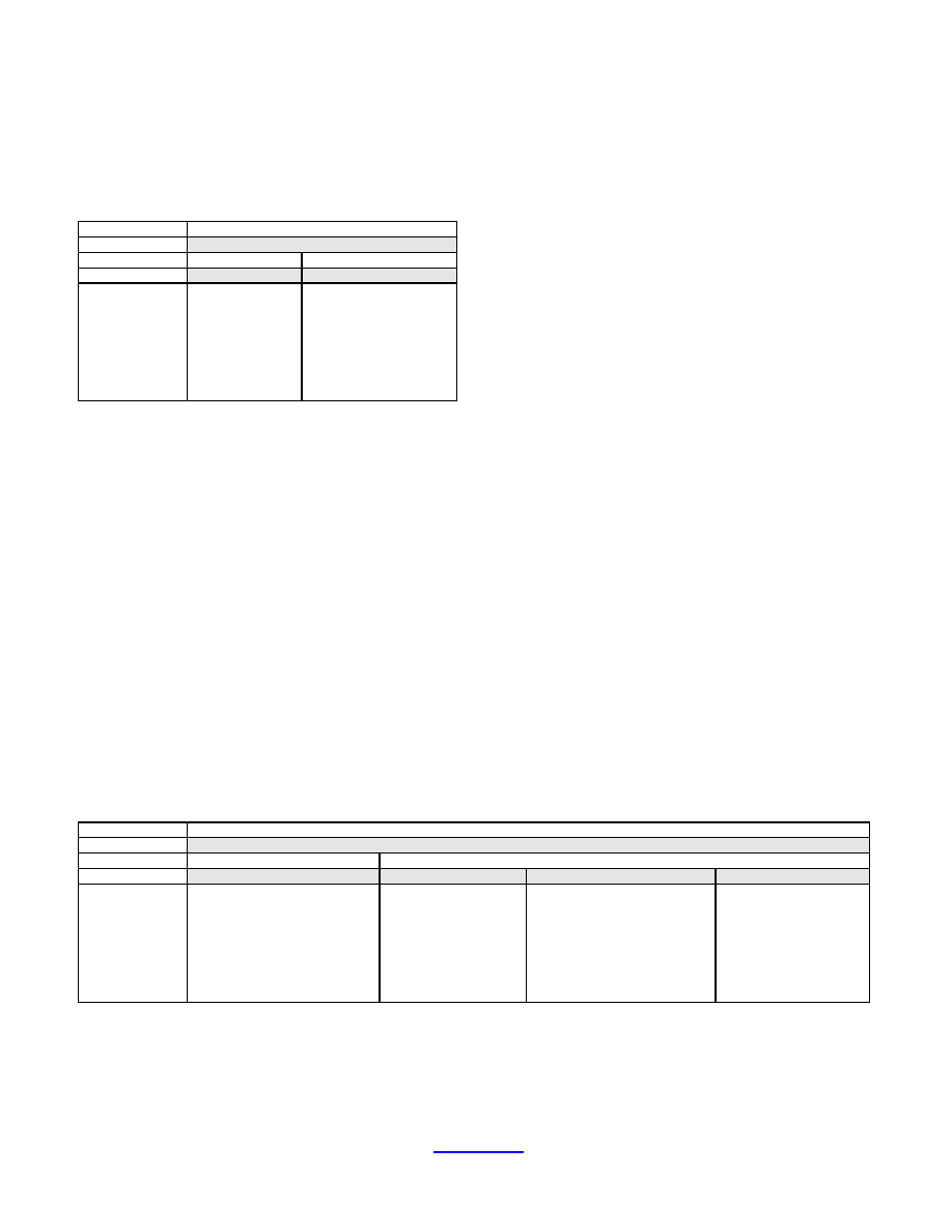
GROUP
J1
FUNCTION
DISPLAY SETTING
PIN
19
20
DISPLAY SET
OPERATION
SWITCHES
SEL0
SEL1
UNIT
MULTIPLIER
DECIMAL
MODE SELECTION
0
0
DGS0
UNT1
±CAL1
J2/NoDec
M1
1
0
DGS1
UNT1
±CAL1
L1DEC
M1
0
1
DGS2
UNT2
±CAL2
L2DEC
M2
1
1
DGS3
UNT3
±CAL3
L3DEC
M3
©
©
©
©
2001 Advanced Linear Devices, Inc., 415 Tasman Drive, Sunnyvale, California 94089-1706, Tel: (408) 747-1155, Fax: (408) 747-1286
ALD523D
12/01
http://
www.aldinc.com
9 of 20
In mode-A operation, the conversion factor "
±CAL1"
parameters resulted from hardware calibration, and they
are scaled through the use of scale factor parameter "N1"
specified inside the DVM523.EXE program. The
"
±CAL2" and "±CAL3" parameters are obtained from
scaling the conversion factor "
±CAL1" through the scale
factor parameters "N2" and "N3" specified inside the
DVM523.EXE program, respectively. See Scale
Conversion Factor (#2 Key) section in the ALD523D
Setup and Calibration Software User Guide on how to
implement these "N1", "N2", and "N3" scale factors.
In mode-B operation, the conversion factor "
±CAL1"
parameters are generated from a ratiometric reference
value from the .MDS file, or from inputting "+CAL1" and
"-CAL1" conversion factors directly into the Input
Conversion Factor screen of the DVM523.EXE via the
keyboard. These conversion factors "
±CAL1" can be
scaled through the scale factor parameter "N1" from the
DVM523.EXE program. The "
±CAL2" and "±CAL3"
parameters are obtained from scaling the conversion factor
"
±CAL1" values through the scale factor parameters "N2"
and "N3" from the same Input Conversion Factor screen,
respectively. See Scale Conversion Factor (#2 Key) or
Input Conversion Factor = CAL1 (
µV/CT) (#M Key)
section in the ALD523D Setup and Calibration Software
User Guide for implementation details.
In mode-C operation, the conversion factor "
±CAL1"
parameter is defined from inputting "+CAL1" and "-
CAL1" conversion factors which are scaleable through the
scale factor parameter "N1" from the Input Conversion
Factor screen of the DVM523.EXE program. The
"
±CAL2" and "±CAL3" parameters are obtained from
scaling the conversion factor "
±CAL1" through the scale
factor parameters "N2" and "N3" from the same Input
Conversion Factor screen. See Input Conversion Factor =
CAL1 (
µV/CT) (#M Key) section in the ALD523D Setup
and Calibration Software User Guide for more
information.
The "UNT1" parameter consists of 8 1-byte hexadecimal
numbers consisting of "UNT11" to "UNT18" parameters
located on the fourth line of the .CDS file (see Table 1 and
Table 3 of the ALD523D Setup and Calibration Software
User Guide for the data sheet layout and the hexadecimal
codes, respectively). When "DGS0" or "DGS1" display
set is selected, each 1-byte hexadecimal number specifies
an alphanumeric character as defined in CG ROM table of
the CDM. When the "UNT11" parameter is set to a space
character (20H), up to a full 7-digit number is displayed
followed by a 7-character label in the UNIT field on the
CDM. Otherwise, a 6-digit number is displayed followed
by an 8-character label in the UNIT field. Similarly,
"UNT2" and "UNT3" parameters can be set up and
displayed on the CDM when "DGS2" and "DGS3" display
sets are selected.
SELECTING AND CONFIGURING DECIMAL
POINT PLACEMENT OR ZERO OFFSET
In mode-A and mode-C operations, the DEC1 and DEC2
switches correspond to the input pins 21 and 23 of the
ALD523D, respectively. They are functionally grouped
into J2. In either mode-A or mode-C operation, DEC1 and
DEC2 switches are jumper hardware switches used to
specify the location of placement of the decimal point of
the displayed reading. DEC1 and DEC2 switch setting
combinations are described in Table 4.
GROUP
J2
FUNCTION
DECIMAL POINT PLACEMENT SETTING
PIN
21
23
SWITCHES
DEC1
DEC2
DECIMAL POINT
PLACEMENT
LOGIC LEVEL
0
0
XXXXXXX
1
0
X . XXXXXX
0
1
XX . XXXXX
1
1
XXX . XXXX
Table 4. Decimal Point setting switch combination for
mode-A and mode-C
.
DEC1 and DEC2 hardware jumper switches are only
functional when display set "DGS0" is selected.
When DEC1=0 and DEC2=0, ALD523D instructs the
display to display the entire number without a decimal
point.
When DEC1=1 and DEC2=0, ALD523D displays the
number with a decimal point placed after the first digit.
When DEC1=0 and DEC2=1, the ALD523D utilizes this
information to display the number with a decimal point
placed after the second digit.
When DEC1=1 and DEC2=1, the ALD523D sets the
display to display the number with a decimal point placed
after the third digit.
This function effectively allows scaling of the displayed
reading. For example, the reading may display 123.456
Volt in one range and 0.123456 KiloVolt in another
display set of the same range.
Decimal placement is also programmed by software
parameters "L1DEC", "L2DEC", "L3DEC" which are
selected as part of display set selections. "L1DEC",

©
©
©
©
2001 Advanced Linear Devices, Inc., 415 Tasman Drive, Sunnyvale, California 94089-1706, Tel: (408) 747-1155, Fax: (408) 747-1286
ALD523D
12/01
http://
www.aldinc.com
10 of 20
"L2DEC", and "L3DEC" are 3 separate decimal point
placement instruction commands, each associated with
display set "DGS1", "DGS2", and "DGS3", respectively.
Each command uses the same format, and has valid
parameters as "00", "01", "02", "03", "04", and "05".
"00" instructs the display module to display no decimal
point. "01" instructs the display module to display a
decimal point after the 1
st
digit. "02" instructs the display
module to display a decimal point after the 2
nd
digit. "03"
instructs the display module to display a decimal point
after the 3
rd
digit. "04" instructs the display module to
display a decimal point after the 4
th
digit. "05" instructs
the display module to display a decimal point after the 5
th
digit.
In mode-B operation, the DEC1and DEC2 switches
change function and become M and Z switches in order to
perform a zero level adjustment. The M and Z switches
correspond to the control input pins 21 and 23 of the
ALD523D, respectively. They are functionally grouped
into J2. M and Z pins set logical states of operations as
described in Table 5.
GROUP
J2
FUNCTION
ZERO LEVEL
PIN
21
23
SWITCHES
M
Z
OPERATION
LOGIC LEVEL
0
X
ZERO LEVEL SHIFTING OFF
1
0
ZERO LEVEL SHIFTING ON
1
1
SET ZERO LEVEL
Table 5. Zero level switch configurations and operations for
mode-B
.
The M switch is the master control switch, which controls
the Z switch. When the M=0, the Z switch function is
disabled, and the zero offset value is included in the
displayed reading. When M=1, zero level shifting is
turned on. At M=1 and Z=1, a zero level is indicated on
the CDM and the zero offset value is stored inside the
controller's memory registers. When the M=1 and Z=0, a
reading with zero level shifting is displayed. In this mode,
the zero offset value previously stored is read back from
the controller's memory registers and subtracted from the
current reading. The displayed reading now has automatic
zero correction. This function is analogous to the TARE
button in many weigh scales.
SELECTING AND CONFIGURING DIGITS
BLANKING
The ALD523D uses B1 and B2 as control-input pins for
setting the "blanking" of the trailing digits of the display's
decimal digits. B1 and B2 switches can be applied in all
modes of operations with 4 combinations as shown in
Table 6. Each logical state combination selects the
numbers of digits to be displayed.
GROUP
J3
FUNCTION
DIGIT BLANKING
PIN
4
5
SWITCHES
B1
B2
NUMBER OF DIGITS
DISPLAYED
LABEL/UNIT
7
CHARACTER
UNIT
8
CHARACTER
UNIT
LOGIC LEVEL
0
0
7-Digits
(XXXXXXX)
6-Digits
(XXXXXX)
1
0
6-Digits
(XXXXXX)
6-Digits
(XXXXXX)
0
1
5-Digits
(XXXXX)
5-Digits
(XXXXX)
1
1
4-Digits
(XXXX)
4-Digits
(XXXX)
Table 6. Blanking switch combination for mode-A, mode-B,
and mode-C
.
When the label/unit "UNT1" or "UNT2" or "UNT3"
parameter is set to 7-characters, at B1=0 and B2=0, the
ALD523D sets the display module to display a full 7-digit
number. When the label/unit "UNT1" or "UNT2" or
"UNT3" parameter is set to 8-characters, at B1=0 and
B2=0, the ALD523D sets the display module to display a
full 6-digit number.
When B1=1 and B2=0, the ALD523D instructs the display
module to blank the last display digit, and the display now
displays a 6-digit number. At B1=0 and B2=1, the
ALD523D blanks the last two digits of the display, and the
display now show only a 5-digit number. Likewise at
B1=1 and B2=1, the ALD523D sets the display to show
only the first 4 digits of the number.
SELECTING AND CONFIGURING
MEASUREMENT SAMPLE AVERAGING
One of the effective techniques to minimize measurement
noise and increase stability is to apply sampling to average
a number of serial data samples. The ALD523D uses this
technique to stabilize its serial data sample reading by
filtering out noise associated with these samples. In
general, the higher the number of serial data samples, the
better the noise rejection, but it also takes longer for the
display to respond to the input changes. A default
recommended sample averaging of 8 offers a good
tradeoff between conversion time and noise rejection.
The ALD523D utilizes DSA1 and DSA2 as control-input
pins for selecting one of three different sets of data
sampling, namely "AVG1", "AVG2", and "AVG3". In all
©
©
©
©
2001 Advanced Linear Devices, Inc., 415 Tasman Drive, Sunnyvale, California 94089-1706, Tel: (408) 747-1155, Fax: (408) 747-1286
ALD523D
12/01
http://
www.aldinc.com
11 of 20
three modes of operations, DSA1 and DSA2 pins on the
ALD523D function as data sample averaging selection
switches. Four DSA1 and DSA2 switch combinations are
described in Table 7. Each logical state combination
selects a pre-defined averaging/sampling.
GROUP
J4
FUNCTION
DATA SAMPLE AVERAGING
PIN
6
7
SWITCHES
DSA1
DSA2
AVERAGE
LOGIC LEVEL
0
0
No Average
(1)
1
0
AVG1
(1, 2, 4, 8, 16, 32, 64, 128)
0
1
AVG2
(1, 2, 4, 8, 16, 32, 64, 128)
1
1
AVG3
(1, 2, 4, 8, 16, 32, 64, 128)
Table 7. Averaging selection switch combination for mode-
A, mode-B, and mode-C
.
When DSA1=0 and DSA2=0, the ALD523D is set to non-
averaging mode. At DSA1=1 and DSA2=0, the
ALD523D utilizes the "AVG1" parameter set at address
02H of the EEPROM memory. At DSA1=0 and DSA2=1,
the ALD523D utilizes "AVG2" at address 03H of the
EEPROM. At DSA1=1 and DSA2=1, the ALD523D
utilizes "AVG3" at address 04H of the EEPROM.
"AVG1", "AVG2", and "AVG3" parameters are 8-bit
hexadecimal numbers at addresses 02H, 03H, and 04H of
the first line of the .CDS file, respectively. Valid "AVG1",
"AVG2" and "AVG3" values are 1, 2, 4, 8, 16, 32, 64, and
128. These values correspond to the number of data
samples averaged.
SELECTING AND CONFIGURING INTEGRATION
TIME
When ALD500/ALD500R and ALD523D are used
together as a chip set, an integration time needs to be
selected for the system. For maximum 50/60-cycle line
power noise rejection, Integration time t
INT
must be picked
as a multiple of the period of the power line frequency.
For example, t
INT
times of 16.667msec, 33.333msec,
50.000msec, 66.667msec, 100msec, 166.67msec,
200msec, and 300msec maximize 60Hz power line noise
rejection. The t
INT
times of 100msec, 200msec, and
300msec maximize 50Hz power line noise rejection.
In general, the longer the integration time, the better the
noise rejection of the power line noise, but it also takes
longer to complete a conversion cycle. Default
recommended integration time of 100msec offers the best
tradeoff of noise performance, conversion time and both
50/60-cycle power line noise rejection. The 100msec
integration time also offers the benefit of being universally
optimal for both 50 and 60 cycles power line noise
rejection.
The ALD523D utilizes S1, S2, and S3 as control-input
pins for selecting different integration times. In mode-A
and mode-B, these switches set different integration time
for different measurement needs based on different R
Int
and C
Int
time constant values (see ALD500/ALD500R data
sheet for more information). However, these three pins
are disabled in mode-C operation. The S1, S2 and S3
logical state combinations are listed in Table 8.
GROUP
J5
FUNCTION
INTEGRATION TIME SELECTION
PIN
3
27
28
SWITCHES
S1
S2
S3
INTEGRATION TIME
APPRX. CONVERSION / SEC
NO. OF 60 Hz CYCLES
LOGIC LEVEL
0
0
0
16.667 ms
10
1
0
0
1
33.333 ms
6.6
2
0
1
0
50.000 ms
5
3
0
1
1
66.667 ms
4
4
1
0
0
100.000 ms
3
6
1
0
1
166.667 ms
2
10
1
1
0
200.000 ms
1.5
12
1
1
1
300.000 ms
1
18
Table 8. Integration time selection switch combination for mode-A and mode-B
.
©
©
©
©
2001 Advanced Linear Devices, Inc., 415 Tasman Drive, Sunnyvale, California 94089-1706, Tel: (408) 747-1155, Fax: (408) 747-1286
ALD523D
12/01
http://
www.aldinc.com
12 of 20
POWER UP AND POWER DOWN
Upon power up or power-on-reset, the ALD523D
initializes all internal counters, registers, I/O ports, and the
CDM. Then it reads the setting of the control-input pins,
and sets up the mode of operation as programmed by
instructions preset by the user in the EEPROM memory.
When the mode of operation has not been preset, a
message "PROGRAM MEMORY" is displayed on the
CDM. Next, it checks the status of the PWRCS pin.
A logical "0" state on PWRCS pin powers up the
ALD523D, and a logical "1" state on the PWRCS pin
powers down the ALD523D as well as the ALD500R
(mode-A) and blanks the CDM (in both mode-A and
mode-B). The crystal oscillator circuit of the ALD523D is
also stopped. To start and power up the ALD523D again,
simply put a logical 0 state on the PWRCS pin. An
external microprocessor can therefore utilize this pin to
control the ALD523D power-on status. If power down
feature is not used, then the PWRCS pin must be grounded
through pull-down resistor to leave the ALD523D in
continuously power-on mode.
REFERENCE CALIBRATION MODE
The ALD523D is designed to interface directly to the
ALD500 or ALD500R integrating dual slope precision
analog processors and work together as a chip set. One of
the beneficial features of the ALD500R to the ALD500 is
its precision internal voltage reference, which eliminates
the need of introducing an external reference voltage to the
conversion system, for equal or improved system
performance along with reduced component count and
cost.
The block diagram of the reference calibration mode is
shown in figure 6. Unlike many external reference voltage
circuits where reference voltage calibration is performed
by tweaking trimmer pots, the internal reference voltage
calibration is performed through the use of software
calibration method, i.e. DVM523.EXE (see Calibrate
Reference Voltage (#3 Key) section in the ALD523D
Setup and Calibration Software User Guide).
Upon power up or during normal running condition, the
ALD523D continuously checks the status of the control-
input pins 18 and 12, namely DVCS and CAL,
respectively for entering setup and calibration modes. A
logical "1" state on DVCS pin and a logical "0" on CAL
pin instruct the ALD523D to enter the reference
calibration mode.
Upon entering reference calibration mode, measurement
data on the ALD523D is transmitted serially to the PC via
SCLK and DATOUT pins. The ALD523D sets the SCLK
pin to logic "0" state with the first bit of the serial data
transmitted simultaneously via DATOUT pin. The PC
reads the first bit on DATOUT and sends a serial clock
pulse on the DVCS line as the acknowledge signal. This
serial data read process continues for the rest of the 24
serial bits with alternatively sending serial clock pulses on
every bit read, until SCLK is set to logic "1" state after 24
clock cycles.
Figure 6. Reference calibration mode block diagram.
The 24-bit serial word corresponding to 24 serial clock
pulses consists of a 23-bit binary word with MSB as the
first bit and LSB the 23
rd
bit, followed by a sign bit as the
last bit. The sign bit is set as logical "1" as a positive sign,
and logical "0" as a negative sign.
Calibration mode can also be used as serial output port
mode, where the output binary word can be clocked out by
any PC, device or microprocessor having access to CAL,
SCLK, DATOUT, and DVCS pins.
The detail calibration timing is shown in "ALD523D to PC
Mode-A Reference Calibration Timing" section of this
data sheet. When CAL pin is set to high at the end of
calibration mode, the ALD523D returns to its normal
continuous running mode.
PC
ALD523D
ALD500R
ANALOG
INPUT
©
©
©
©
2001 Advanced Linear Devices, Inc., 415 Tasman Drive, Sunnyvale, California 94089-1706, Tel: (408) 747-1155, Fax: (408) 747-1286
ALD523D
12/01
http://
www.aldinc.com
13 of 20
EEPROM MEMORY
The ALD523D is organized to operate in conjunction with
a 1K (128 bytes x 8 bits) bi-directional two-wire serial
interface protocol EEPROM memory with page write (8
bytes) capability and has a typical 2 ms write cycle time
for page write, i.e. the 24LC01B or compatible. The
ALD523D stores its setup parameters and arithmetic
parameters at specific memory address locations of the
EEPROM. These parameters are transferred from
DVM523.EXE PC software to the internal registers of the
ALD523D via a standard PC parallel printer port, and are
page written to the EEPROM from the ALD523D's
internal registers via serial address/data I/O (SDA) and
serial clock (SCL) lines. Once initiated, all data transfers
between the PC to ALD523D and then to the EEPROM
are performed on a handshake basis automatically. The
setup parameters are predefined inside the .CDS file,
where the arithmetic parameters are obtained from
calibration process and/or conversion factor scaling.
DATA TRANSFER MODE FROM PC TO ALD523D
The setup parameters and arithmetic parameters of the
ALD523D are stored at the specific memory address
locations as depicted in Table 1 of the ALD523D Setup
and Calibration Software User Guide, and uploaded to the
EEPROM from PC via a parallel printer port (see Upload
Page 1 To 6 (#4 Key) or Upload Page 1 To 13 (#5Key) To
Memory section in the ALD523D Setup and Calibration
Software User Guide on how to upload EEPROM via
DVM523.EXE). The block diagram of the data transfer
mode is shown in figure 7.
Figure 7. Data transfer mode block diagram.
Upon power up or during normal running condition, the
ALD523D continuously checks the status of DVCS and
CAL, respectively for the setup and calibration mode. A
logical "0" state on DVCS pin with a logical "0" on CAL
pin set by the PC put the ALD523D in the Data Transfer
from PC mode.
In this mode, a message "UPLOAD MEMORY" is
displayed on the Characters Display Module (CDM) to
indicate the ALD523D is in data transfer mode.
Parameters for uploading EEPROM are transferred from
the PC to ALD523D serially via the SCLK and DATIN
pins, with 8 bytes of 8-bit data (total of 64 bits) as 1 page
of data.
Initially, the bit and page counters within the ALD523D
and the PC are set to 1, and the DVCS pin is set to logic
"0" state with the first bit of the serial data transmitted
simultaneously via DATIN pin. The ALD523D reads the
first bit on DATIN and sends a serial clock pulse on the
SCLK as the acknowledge signal. This serial data upload
process continues for the rest of the 64 serial bits with
alternatively receiving the DVCS pulses from the PC and
sending the corresponding serial clock pulses on every bit
read, until the bit counter is set to 64 along with DVCS set
to logic "1" state, which then are in turn uploaded into the
EEPROM automatically by the ALD523D, using the page
write mode.
Then the page counter is advanced to the second page, and
the PC puts out a second DVCS logic "0" state, and begins
the transfer of the next 8 bytes of 8-bit data. Through the
repeated serial clock and data valid handshakes via DVCS
and SCLK pins, either 6 pages or 13 pages of 8 bytes of 8-
bit serial data are transmitted via DATIN pin into
ALD523D's internal registers. This uploading process is
fully automatic.
The 64-bit serial clock pulses transmit 64-bit binary data
with bit 63 as the first bit and bit 0 as the last bit. The
detailed timing is shown in "Data Transfer From PC"
section of this data sheet. Once the PC sets the CAL pin to
logic "1" at the end of setup mode, the ALD523D returns
to its normal running mode.
ALD523D
1K
EEPROM
PC
INTERFACE

©
©
©
©
2001 Advanced Linear Devices, Inc., 415 Tasman Drive, Sunnyvale, California 94089-1706, Tel: (408) 747-1155, Fax: (408) 747-1286
ALD523D
12/01
http://
www.aldinc.com
14 of 20
DEFAULT PULL-UP AND PULL-DOWN
RESISTORS
Switches or jumpers can be used to interface the
ALD523D control-input pins directly to the desired logic
level, either V
+
or DGND, through 15-k
pull-up and 1-
K
pull-down resistors. This method of connection is
adopted as a default (standard) connection.
Figure 8 shows an example of standard connection where
a switch SW or a jumper is used to pull the display set
selection SEL1 control-input pin down to logic level "0"
through a 1-k
pull-down resistor to GND with the switch
SW closed. The SEL1 control-input pin is pulled up to
logic level "1" through a 15-k
pull-up resistor to V
+
with
the switch SW opened.
This method of connection allows both pull-up and pull-
down resistors to be installed simultaneously. When
switch SW is closed, the pin is normally at a logical "0"
state, which sets SEL1=0. However, when ALD523D is
transferring data to the CDM, the same pin changes
function from SEL1 to D1, and the ALD523D output
overrides both the pull-up and pull-down resistors. All the
other multiplexed pins that interface to the CDM are
multiplexed in the same way.
Figure 8. 15-k
pull-up or 1-k
pull-down resistor
connection via SW switch.
CHARACTER DISPLAY MODULE
The ALD523D controller is designed for easy setting of
industry standard Character Display Modules (CDM) such
as 1 line by 16-character or 2-line by 16-character LCD or
VFD display modules. These Character Display Modules
consist of high contrast liquid crystal or vacuum
fluorescence panels.
Each module contains an industry standard controller such
as HD44780 or equivalent, and all necessary drivers. This
industry standard controller is equipped with an internal
Character Generator (CG ROM and CG RAM), Display
Data (DD RAM), and Column Driver such as LC7930N or
equivalent. ALD523D contains all the necessary display
function instructions of the CDM to fully display all the
characters on the display line(s), and to access all the
available alphanumeric characters within the CG ROM.
Standard font version of CGROM, European font version
of CGROM, or other custom versions of CGROM can be
used with ALD523D. For more information, consult with
the CDM manufacturer's technical data.
R-PullUp = 15K
R-PullDown = 1K
PMOS
NMOS
LCD or VFD
ALD523D
19
SEL0/D0
20
SEL1/D1
U1
SW
+V
+V
R-PullDown
R-PullUp
©
©
©
©
2001 Advanced Linear Devices, Inc., 415 Tasman Drive, Sunnyvale, California 94089-1706, Tel: (408) 747-1155, Fax: (408) 747-1286
ALD523D
12/01
http://
www.aldinc.com
15 of 20
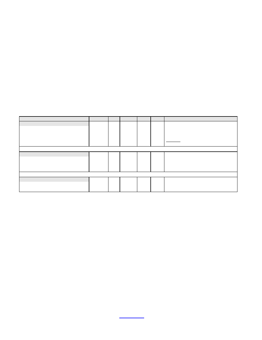
ABSOLUTE MAXIMUM RATINGS
3
Supply voltage, V
+
_______________________________________________________________________________ +6.7V
Differential input voltage range ____________________________________________________________ -0.3 to V
+
+ 0.3V
Power dissipation ________________________________________________________________________________ 1.2 W
Operating temperature range __________________________________________________________________ 0
o
C to +70
o
C
Storage temperature range _________________________________________________________________ -65
o
C to +150
o
C
Lead temperature, 10 seconds _____________________________________________________________________ +260
o
C
Maximum allowable output current sinked by any I/O pin _________________________________________________25mA
Maximum allowable output current sourced by any I/O pin ________________________________________________25mA
DC OPERATING ELECTRICAL CHARACTERISTICS
T
A
= 0
o
C - 70
o
C, V
+
= +5V, f
XTL
= 3.6864 MHz unless otherwise specified
Parameter
Symbol
Min
Typ
Max
Unit
Test Conditions
Supply
Operating Voltage Range
V
+
3
5
5.5
V
Supply Current
I
DD
6.5
8.0
mA
Supply Current
I
DD
2
mA
V
+
= 3.5V
Shutdown Mode Supply Current
I
SDD
3
10
µA
PWRCS = +5V, V
IN
= 0V
Input Characteristics
Low Input Voltage
V
IL
-0.3
1.0
V
High Input Voltage
V
IH
3.5
5.3
V
Input Leakage Current
I
IL
-1
2
µA
Output Characteristics
Low Output Voltage
V
OL
0.2
0.4
V
I
out
= 4 mA
High Output Voltage
V
OH
4.6
4.8
V
I
out
= -2 mA
©
©
©
©
2001 Advanced Linear Devices, Inc., 415 Tasman Drive, Sunnyvale, California 94089-1706, Tel: (408) 747-1155, Fax: (408) 747-1286
ALD523D
12/01
http://
www.aldinc.com
16 of 20
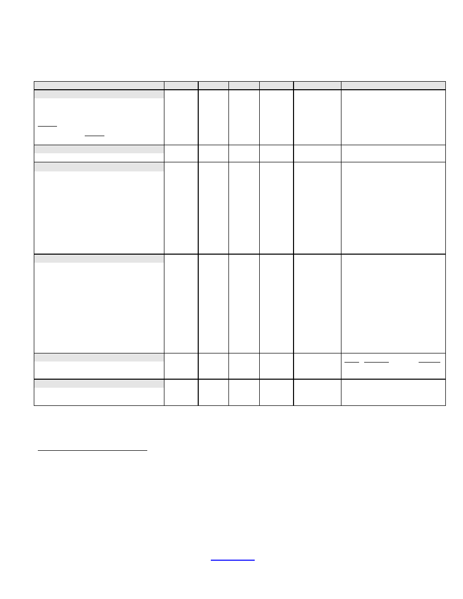
TIMING CHARACTERISTICS
T
A
= 0
o
C - 70
o
C, V
+
= +5V, f
XTL
= 3.6864 MHz, internal system clock = f
XTL
/4 unless otherwise specified
Parameter
Symbol
Min
Typ
Max
Unit
Test Conditions
Display Only (Mode-C) Timing
DATIN Setup Time
t
DS
3.7
µs
Serial Clock Low Time
t
SCL
16.2
µs
Serial Clock High Time
t
SCH
67.6
µs
DVCS to DATIN Valid Time
t
DIV
67.62
µs
Serial Clock to DVCS High Time
t
DVCSH
22.22
µs
Power Timing
Power-On-Reset Time
t
POR
2
sec
Data Transfer From PC Timing
4
Calibration to Data Valid Time
t
CALDV
1.9
µs
Serial Clock High Time
t
SCLKH
67
µs
Serial Clock Low Time
t
SCLKL
10
µs
Data Valid to Serial Clock Delay Time
t
DSdelay
0.271
500,000
µs
Serial Clock to Data Valid High Time
t
SCDVH
0
DC
ns
Serial Clock to Data Valid Low Time
t
SCDVL
0
DC
ns
DATIN Setup Time
t
DS
2.4
µs
Data Valid High Time
t
DVH
10
µs
Serial Clock to Calibration Time
t
SCCAL
0
8
ms
Reference Calibration Timing
Auto Zero Time
t
AZ
t
INT
ms
Integration Time
1, 2
t
INT
16.667
300
ms
Integrator Zero Time
t
INTZ
2
ms
Calibration Setup Time
t
CS
1.1
µs
Calibration Delay Time
5
t
CD
1
Conv. Cycle
DATOUT Valid Setup Time
t
DVS
18
µs
DATOUT Not Valid Time
t
DNV
15
µs
DATOUT Valid Time
t
DV
11
µs
DATOUT Valid Time Out Time
t
TO
5.5
ms
DATOUT Out Time
t
DATOUT
500
ns
Input / Output Characteristic Timing
Input Interrupt Low Time
t
IL
70
ns
CAL, PWRCS, COUT, DVCS
Rise/Fall Times (CL = 10pF)
t
R
, t
F
25
125
ns
Oscillator (OSC
IN
, OSC
OUT
)
Crystal Frequency
f
XTL
3.6864
8
MHz
External Frequency (OSC
IN
)
f
OSC
8
MHz
Rise time/Fall time
15 ns
1
Apply only for calibrated reference (mode-A) and ratiometric (mode-B) operations.
2
Extendible from S1, S2, and S3 hardware switches through "SETF" parameter in the .CDS file. Lower integration time than the
minimum allows more conversion cycles per second at reduced count resolution. Higher integration time increases count resolution,
but requires increased capacitor value and lowered number of conversion cycles per second. De-integration time depends on
selection of full scale input range, integration capacitor value and voltage reference.
3
ESD Sensitive Device. Stresses above those listed under Absolute Maximum Ratings may cause permanent damage to
device, and may affect device reliability and performance.
4
PC to ALD523D handshake using page write mode.
5
Calibration delay time (t
CD
) may be as short as 7
µs, if start of auto zero phase cycle time could be determined. For asynchronous
operation, t
CD
must be for a minimum of one complete conversion cycle to assure synchronization to start of auto zero phase cycle time.
©
©
©
©
2001 Advanced Linear Devices, Inc., 415 Tasman Drive, Sunnyvale, California 94089-1706, Tel: (408) 747-1155, Fax: (408) 747-1286
ALD523D
12/01
http://
www.aldinc.com
17 of 20
DISPLAY ONLY (MODE-C) TIMING
*Note: Default mode is SCLK, which can be inverted to produce SCLK by software setup.
DATA TRANSFER FROM PC TIMING
________________________________________
∑
n is the number of serial data bits, and m is the integer of 1, 2, ..., n.
DATIN
IN FROM
SERIAL
SOURCE
t
DS
t
SCH
t
DIV
DVCS
IN FROM SERIAL
SOURCE
SCLK*
OUT TO
SERIAL
SOURCE
t
DS
t
SCL
S S
S S
t
DVCSH
S S
MSB BIT
BIT n-2
LSB BIT
SIGN BIT
NOT VALID
S S
BIT n-m
NOT VALID
DVCS
IN FROM PC
CAL
IN FROM PC
S S
t
DVH
t
CALDV
t
SCDVL
t
SCLKH
SCLK
OUT TO PC
t
SCLKL
t
DSdelay
t
SCDVH
S S
S S
DATIN
IN FROM PC
BIT 63
BIT 62
NOT VALID
BIT 0
t
DS
t
DS
S S
S S
NOT VALID
BIT n-m
NOT VALID
t
SCCAL
t
CALDV
©
©
©
©
2001 Advanced Linear Devices, Inc., 415 Tasman Drive, Sunnyvale, California 94089-1706, Tel: (408) 747-1155, Fax: (408) 747-1286
ALD523D
12/01
http://
www.aldinc.com
18 of 20
ALD523D TO PC MODE-A REFERENCE CALIBRATION TIMING
EXPANDED VIEW
DATOUT
OUT TO PC
t
AZ
t
INT
A
OUT TO
ALD500
B
OUT TO
ALD500
COUT
IN FROM
ALD500
t
DINT
t
INTZ
t
AZ
SCLK
OUT TO PC
t
DNV
t
DV
t
TO
CAL
IN FROM PC
t
CS
t
DVS
DVCS
IN FROM PC
SIGN BIT
NOT VALID
BIT 0
(LSB)
BIT 22
(MSB)
t
DATOUT
NOT VALID
NOT
VALID
NOT
VALID
NOT
VALID
S S
S S
S S
S S
S S
S S
S S
S S
S S
S S
S S
DATOUT
OUT TO PC
SCLK
OUT TO PC
t
DNV
t
DV
DVCS
IN FROM PC
t
TO
SIGN BIT
NOT VALID
BIT 0
(LSB)
BIT 22
(MSB)
t
DATOUT
NOT VALID
NOT VALID
NOT VALID
NOT VALID
S S
S S
S S
S S
©
©
©
©
2001 Advanced Linear Devices, Inc., 415 Tasman Drive, Sunnyvale, California 94089-1706, Tel: (408) 747-1155, Fax: (408) 747-1286
ALD523D
12/01
http://
www.aldinc.com
19 of 20
ALD523D PIN IDENTIFICATION FOR CALIBRATED REFERENCE MODE (MODE-A)
PIN #
SYMBOL
FUNCTION
SIGNAL PROPAGATION
1
COUT
COMPARATOR OUTPUT
INPUT
2
SDA
MEMORY SERIAL ADDRESS/DATA
INPUT/OUTPUT
3
S1, SCL
INTEGRATION TIME SWITCH, MEMORY SERIAL CLOCK
INPUT/ OUTPUT
4
B1, D4
BLANK SWITCH, DISPLAY DATA BIT
INPUT/OUTPUT
5
B2, D5
BLANK SWITCH, DISPLAY DATA BIT
INPUT/OUTPUT
6
DSA1, D6
AVERAGING SWITCH, DISPLAY DATA BIT
INPUT/OUTPUT
7
DSA2, D7
AVERAGING SWITCH, DISPLAY DATA BIT
INPUT/OUTPUT
8
V
+
POWER SUPPLY
9
XTAL2
CRYSTAL OSCILLATOR
OUTPUT
10
XTAL1
CRYSTAL OSCILLATOR
INPUT
11
COUT
COMPARATOR OUTPUT
INPUT INTERRUPT
12
CAL
CALIBRATION SIGNAL
INPUT
13
PWRCS
POWER UP CHIP SELECT
INPUT
14
CS
CHIP SELECT
OUTPUT
15
B
A/D INPUT
OUTPUT
16
WP
MEMORY WRITE PROTECT
OUTPUT
17
A
A/D INPUT
OUTPUT
18
DVCS
DATA VALID CHIP SELECT
INPUT
19
SEL0, D0
MODE SWITCH, DISPLAY DATA BIT
INPUT/OUTPUT
20
SEL1, D1
MODE SWITCH, DISPLAY DATA BIT
INPUT/OUTPUT
21
DEC1, D2
DECIMAL POSITION SWITCH, DISPLAY DATA BIT
INPUT/OUTPUT
22
DGND
DIGITAL GROUND
23
DEC2, D3
DECIMAL POSITION SWITCH, DISPLAY DATA BIT
INPUT/OUTPUT
24
DATIN
DATA IN
INPUT
25
SCLK
SERIAL CLOCK
OUTPUT
26
DATOUT
DATA OUT
OUTPUT
27
S2, EN
INTEGRATION TIME SWITCH, DISPLAY ENABLE
INPUT/OUTPUT
28
S3, RS
INTEGRATION TIME SWITCH, DISPLAY REGISTER SELECT
INPUT/OUTPUT
ALD523D PIN IDENTIFICATION FOR RATIOMETRIC MODE (MODE-B)
PIN #
SYMBOL
FUNCTION
SIGNAL PROPAGATION
1
COUT
COMPARATOR OUTPUT
INPUT
2
SDA
MEMORY SERIAL ADDRESS/DATA
INPUT/OUTPUT
3
S1, SCL
INTEGRATION TIME SWITCH, MEMORY SERIAL CLOCK
INPUT/ OUTPUT
4
B1, D4
BLANK SWITCH, DISPLAY DATA BIT
INPUT/OUTPUT
5
B2, D5
BLANK SWITCH, DISPLAY DATA BIT
INPUT/OUTPUT
6
DSA1, D6
AVERAGING SWITCH, DISPLAY DATA BIT
INPUT/OUTPUT
7
DSA2, D7
AVERAGING SWITCH, DISPLAY DATA BIT
INPUT/OUTPUT
8
V
+
POWER SUPPLY
9
XTAL2
CRYSTAL OSCILLATOR
OUTPUT
10
XTAL1
CRYSTAL OSCILLATOR
INPUT
11
COUT
COMPARATOR OUTPUT
INPUT INTERRUPT
12
CAL
CALIBRATION SIGNAL
INPUT
13
PWRCS
POWER UP CHIP SELECT
INPUT
14
CS
CHIP SELECT
OUTPUT
15
B
A/D INPUT
OUTPUT
16
WP
MEMORY WRITE PROTECT
OUTPUT
17
A
A/D INPUT
OUTPUT
18
DVCS
DATA VALID CHIP SELECT
INPUT
19
SEL0, D0
MODE SWITCH, DISPLAY DATA BIT
INPUT/OUTPUT
20
SEL1, D1
MODE SWITCH, DISPLAY DATA BIT
INPUT/OUTPUT
21
M, D2
ZERO MASTER SWITCH, DISPLAY DATA BIT
INPUT/OUTPUT
22
DGND
DIGITAL GROUND
23
Z, D3
ZERO SWITCH, DISPLAY DATA BIT
INPUT/OUTPUT
24
DATIN
DATA IN
INPUT
25
SCLK
SERIAL CLOCK
OUTPUT
26
DATOUT
DATA OUT
OUTPUT
27
S2, EN
INTEGRATION TIME SWITCH, DISPLAY ENABLE
INPUT/OUTPUT
28
S3, RS
INTEGRATION TIME SWITCH, DISPLAY REGISTER SELECT
INPUT/OUTPUT

©
©
©
©
2001 Advanced Linear Devices, Inc., 415 Tasman Drive, Sunnyvale, California 94089-1706, Tel: (408) 747-1155, Fax: (408) 747-1286
ALD523D
12/01
http://
www.aldinc.com
20 of 20
ALD523D PIN IDENTIFICATION FOR DISPLAY ONLY MODE (MODE-C)
PIN #
SYMBOL
FUNCTION
SIGNAL PROPAGATION
1
-
-
-
2
SDA
MEMORY SERIAL ADDRESS/DATA
INPUT/OUTPUT
3
SCL
MEMORY SERIAL CLOCK
OUTPUT
4
B1, D4
BLANK SWITCH, DISPLAY DATA BIT
INPUT/OUTPUT
5
B2, D5
BLANK SWITCH, DISPLAY DATA BIT
INPUT/OUTPUT
6
DSA1, D6
AVERAGING SWITCH, DISPLAY DATA BIT
INPUT/OUTPUT
7
DSA2, D7
AVERAGING SWITCH, DISPLAY DATA BIT
INPUT/OUTPUT
8
V
+
POWER SUPPLY
9
XTAL2
CRYSTAL OSCILLATOR
OUTPUT
10
XTAL1
CRYSTAL OSCILLATOR
INPUT
11
-
-
-
12
CAL
CALIBRATION SIGNAL
INPUT
13
PWRCS
POWER UP CHIP SELECT
INPUT
14
-
-
-
15
-
-
-
16
WP
MEMORY WRITE PROTECT
OUTPUT
17
-
-
-
18
DVCS
DATA VALID CHIP SELECT
INPUT
19
SEL0, D0
MODE SWITCH, DISPLAY DATA BIT
INPUT/OUTPUT
20
SEL1, D1
MODE SWITCH, DISPLAY DATA BIT
INPUT/OUTPUT
21
DEC1, D2
DECIMAL POSITION SWITCH, DISPLAY DATA BIT
INPUT/OUTPUT
22
DGND
DIGITAL GROUND
23
DEC2, D3
DECIMAL POSITION SWITCH, DISPLAY DATA BIT
INPUT/OUTPUT
24
DATIN
DATA IN
INPUT
25
SCLK
SERIAL CLOCK
OUTPUT
26
DATOUT
DATA OUT
OUTPUT
27
EN
DISPLAY ENABLE
OUTPUT
28
RS
DISPLAY REGISTER SELECT
OUTPUT