2003
THRU
2024
x = digit to identify specific device. Characteristic shown applies to family of
devices with remaining digits as shown. See matrix on next page.
Data Sheet
29304F
Ideally suited for interfacing between low-level logic circuitry and
multiple peripheral power loads, the Series ULN20xxA/L high-voltage,
high-current Darlington arrays feature continuous load current ratings
to 500 mA for each of the seven drivers. At an appropriate duty cycle
depending on ambient temperature and number of drivers turned ON
simultaneously, typical power loads totaling over 230 W (350 mA x 7,
95 V) can be controlled. Typical loads include relays, solenoids,
stepping motors, magnetic print hammers, multiplexed LED and
incandescent displays, and heaters. All devices feature open-collector
outputs with integral clamp diodes.
The ULN2003A/L and ULN2023A/L have series input resistors
selected for operation directly with 5 V TTL or CMOS. These devices
will handle numerous interface needs -- particularly those beyond the
capabilities of standard logic buffers.
The ULN2004A/L and ULN2024A/L have series input resistors for
operation directly from 6 to 15 V CMOS or PMOS logic outputs.
The ULN2003A/L and ULN2004A/L are the standard Darlington
arrays. The outputs are capable of sinking 500 mA and will withstand
at least 50 V in the OFF state. Outputs may be paralleled for higher
load current capability. The ULN2023A/L and ULN2024A/L will
withstand 95 V in the OFF state.
These Darlington arrays are furnished in 16-pin dual in-line plastic
packages (suffix "A") and 16-lead surface-mountable SOICs (suffix
"L"). All devices are pinned with outputs opposite inputs to facilitate
ease of circuit board layout. All devices are rated for operation over the
temperature range of -20
�C to +85�C. Most (see matrix, next page) are
also available for operation to -40
�C; to order, change the prefix from
"ULN" to "ULQ".
FEATURES
I TTL, DTL, PMOS, or CMOS-Compatible Inputs
I Output Current to 500 mA
I Output Voltage to 95 V
I Transient-Protected Outputs
I Dual In-Line Plastic Package or Small-Outline IC Package
HIGH-VOLTAGE, HIGH-CURRENT
DARLINGTON ARRAYS
Dwg. No. A-9594
16
15
14
13
12
6
11
7
10
8
9
1
2
3
4
5
Note that the ULN20xxA series (dual in-line
package) and ULN20xxL series (small-outline
IC package) are electrically identical and share
a common terminal number assignment.
ABSOLUTE MAXIMUM RATINGS
Output Voltage, V
CE
(ULN200xA and ULN200xL) ........ 50 V
(ULN202xA and ULN202xL) ........ 95 V
Input Voltage, V
IN
................................ 30 V
Continuous Output Current,
I
C
................................................. 500 mA
Continuous Input Current, I
IN
........... 25 mA
Power Dissipation, P
D
(one Darlington pair) ..................... 1.0 W
(total package) ....................... See Graph
Operating Temperature Range,
T
A
.................................. -20
�
C to +85
�
C
Storage Temperature Range,
T
S
................................. -55
�
C to +150
�
C
2003
THRU
2024
HIGH-VOLTAGE,
HIGH-CURRENT
DARLINGTON ARRAYS
115 Northeast Cutoff, Box 15036
Worcester, Massachusetts 01615-0036 (508) 853-5000
V
CE(MAX)
50 V
95 V
I
C(MAX)
500 mA500 mA
Logic
Part Number
5V
ULN2003A*
ULN2023A*
TTL, CMOS
ULN2003L*
ULN2023L
6-15 V
ULN2004A*
ULN2024A
CMOS, PMOS
ULN2004L*
ULN2024L
* Also available for operation between -40
�C and +85�C. To order, change
prefix from "ULN" to "ULQ".
Dwg. No. A-9651
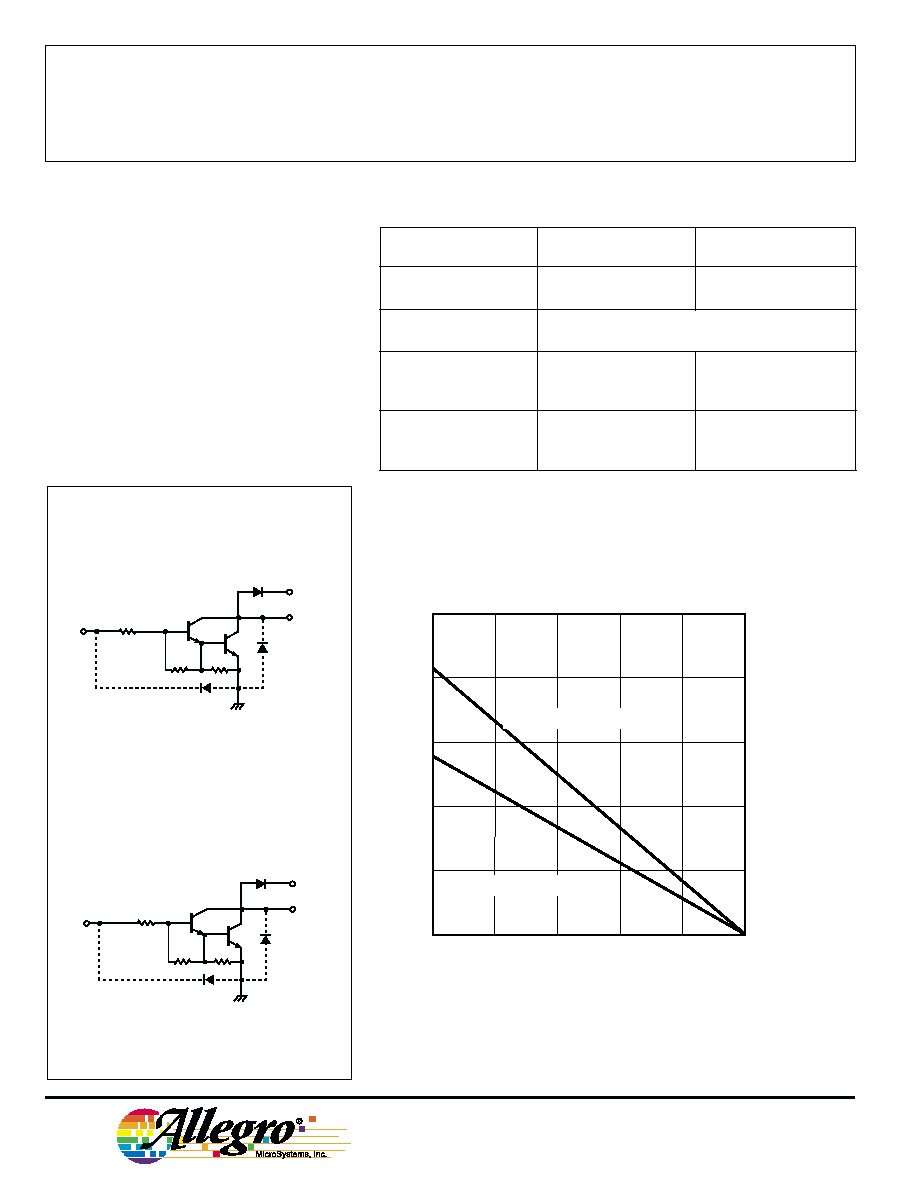
COM
7.2K
3K
2.7K
X = Digit to identify specific device. Specification shown applies to family of
devices with remaining digits as shown. See matrix above.
Copyright � 1974, 1998 Allegro MicroSystems, Inc.
Dwg. No. A-9898A
ULN20x4A/L (Each Driver)
COM
7.2K
3K
10.5K
50
75
100
125
150
2.5
0.5
0
ALLOWABLE PACKAGE POWER DISSIPATION IN WATTS
AMBIENT TEMPERATURE IN
�C
2.0
1.5
1.0
25
SUFFIX 'L', R = 90
�C/W
JA
Dwg. GP-006A
SUFFIX 'A', R = 60
�C/W
JA
ULN20x3A/L (Each Driver)
DEVICE PART NUMBER DESIGNATION
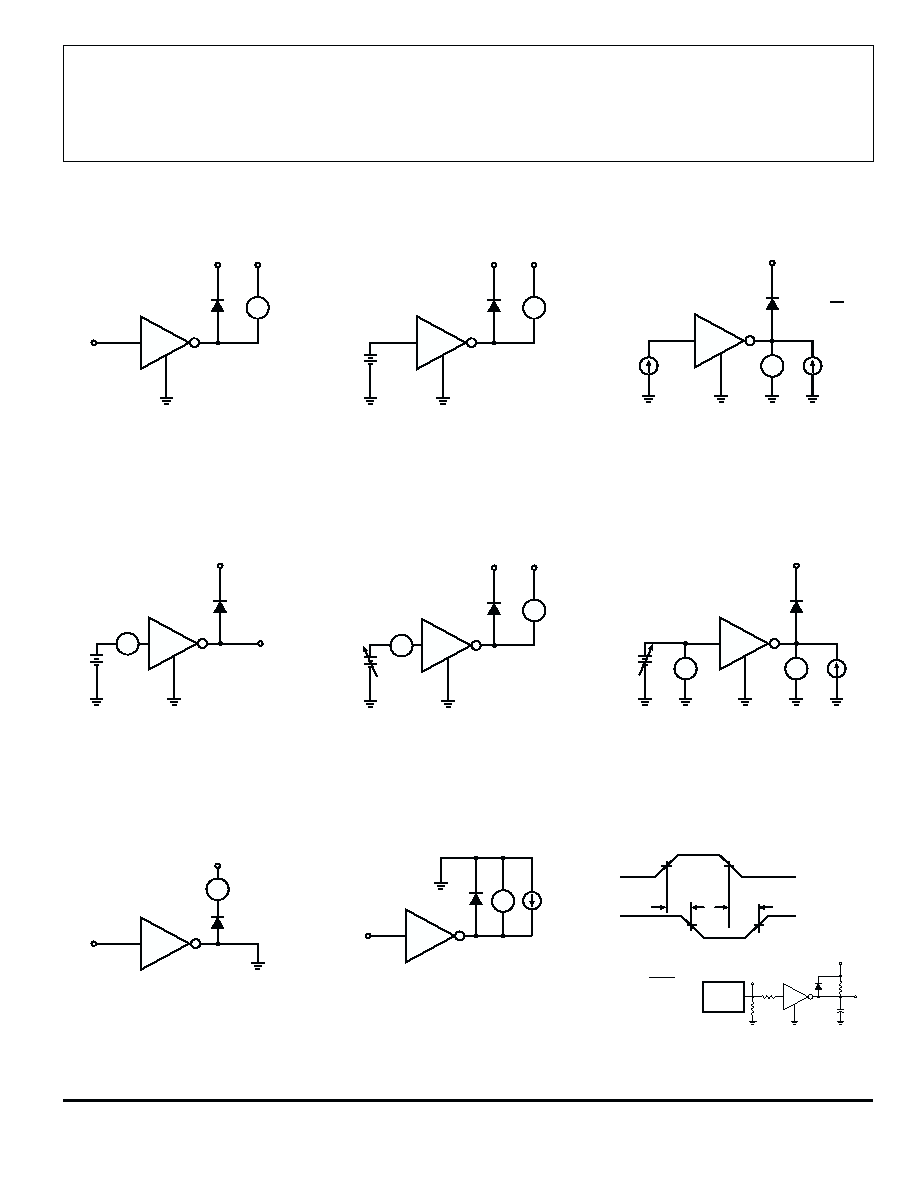
PARTIAL SCHEMATICS
2003
THRU
2024
HIGH-VOLTAGE,
HIGH-CURRENT
DARLINGTON ARRAYS
115 Northeast Cutoff, Box 15036
Worcester, Massachusetts 01615-0036 (508) 853-5000
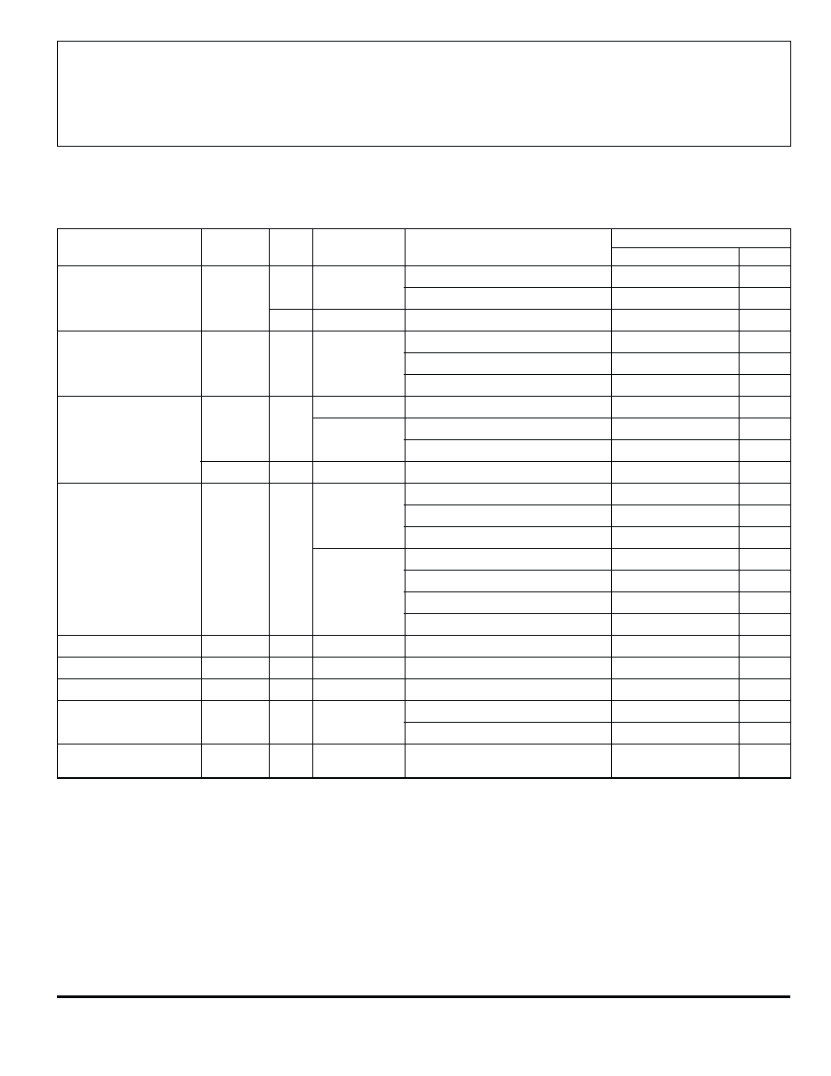
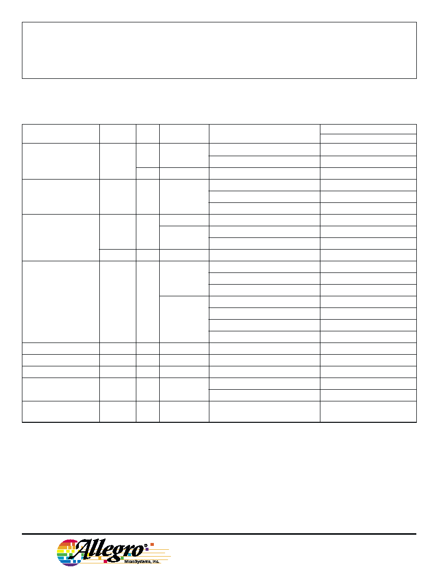
Test
Applicable
Limits
Characteristic
Symbol
Fig.
Devices
Test Conditions
Min.
Typ.
Max.
Units
Output Leakage Current
I
CEX
1AA
ll
V
CE
= 95 V, T
A
= 25
�C
--
< 1
50
�A
V
CE
= 95 V, T
A
= 70
�C
--
< 1
100
�A
1B
ULN2024A/L
V
CE
= 95 V, T
A
= 70
�C, V
IN
= 1.0 V
--
< 5
500
�A
Collector-Emitter
V
CE(SAT)
2
A
ll
I
C
= 100 mA, I
B
= 250
�A--
0.9
1.1
V
Saturation Voltage
l
C
= 200 mA, I
B
= 350
�A--
1.1
1.3
V
I
C
= 350 mA, I
B
= 500
�A--
1.3
1.6
V
Input Current
I
IN(ON)
3
ULN2023A/L
V
IN
= 3.85 V
--
0.93
1.35
mA
ULN2024A/L
V
IN
= 5.0 V
--
0.35
0.5
mA
V
IN
= 12 V
--
1.0
1.45
mA
I
IN(OFF)
4
A
ll
l
C
= 500
�A, T
A
= 70
�C
50
65
--
�A
Input Voltage
V
IN(ON)
5
ULN2023A/L
V
CE
= 2.0 V, l
C
= 200 mA--
--
2.4
V
V
CE
= 2.0 V, I
C
= 250 mA--
--
2.7
V
V
CE
= 2.0 V, l
C
= 300 mA--
--
3.0
V
ULN2024A/L
V
CE
= 2.0 V, l
C
= 125 mA--
--
5.0
V
V
CE
= 2.0 V, l
C
= 200 mA--
--
6.0
V
V
CE
= 2.0 V, I
C
= 275 mA--
--
7.0
V
V
CE
= 2.0 V, l
C
= 350 mA--
--
8.0
V
Input Capacitance
C
IN
--
A
ll
--
15
25
pF
Turn-On Delay
t
PLH
8
All
0.5 E
IN
to 0.5 E
OUT
--
0.25
1.0
�s
Turn-Off Delay
t
PHL
8
All
0.5 E
IN
to 0.5 E
OUT
--
0.25
1.0
�s
Clamp Diode
I
R
6
A
ll
V
R
= 95 V, T
A
= 25
�C
--
--
50
�A
Leakage Current
V
R
= 95 V, T
A
= 70
�C
--
--
100
�A
Clamp Diode
V
F
7
A
ll
I
F
= 350 mA--
1.7
2.0
V
Forward Voltage
Complete part number includes suffix to identify package style: A = DIP, L = SOIC.
Types ULN2023A, ULN2023L, ULN2024A, and ULN2024L
ELECTRICAL CHARACTERISTICS at +25
�
C (unless otherwise noted).