QUAD 1.5 A DARLINGTON SWITCHES
High-voltage, high-current Darlington arrays ULN2064B/LB
through ULN2069B/LB are designed for interface between low-level
logic and a variety of peripheral loads such as relays, solenoids, dc and
stepper motors, magnetic print hammers, multiplexed LED and incan-
descent displays, heaters, and similar loads. Output off voltage ratings
of 50 V and 80 V are available. These quad drivers can drive resistive
loads to 480 watts (1.5 A x 80 V, 26% duty cycle). For inductive
loads, sustaining voltages of 35 V and 50 V at 100 mA are specified.
Quad drivers ULN2064B/LB, ULN2065B/LB, ULN2068B/LB,
and ULN2069B/LB are intended for use with TTL, low-speed TTL,
and 5 V MOS logic. The ULN2065B/LB and ULN2069B/LB are
selected for the 80 V minimum output breakdown specification. The
ULN2068B/LB and ULN2069B/LB have pre-driver stages and are
recommended for applications requiring high gain (low input-current
loading). Quad-driver arrays are supplied with heat-sink contact tabs
in 16-pin plastic DlPs (suffix `B') and 20-lead surface-mountable wide-
body SOICs (suffix `LB').
FEATURES
I TTL, DTL, MOS, CMOS Compatible Inputs
I Transient-Protected Outputs
I Loads to 480 Watts
I Heat-Sink Contact Tabs
I Automotive Capable
ABSOLUTE MAXIMUM RATINGS
at +25
∞
C Free-Air Temperature
for Any One Driver
(unless otherwise noted)
Output Voltage, V
CEX
................ See Guide
Output Sustaining Voltage,
V
CE(SUS)
............................. See Guide
Output Current, I
OUT
(Note 1) .......... 1.75 A
Input Voltage, V
IN
...................... See Guide
Input Current, I
B
(Note 2) .................. 25 mA
Supply Voltage,
V
S
(ULN2068B/LB & 2069B/LB) ... 10 V
Total Package Power Dissipation,
P
D
....................................... See Graph
Operating Temperature Range,
T
A
................................. -20
∞
C to +85
∞
C
Storage Temperature Range,
T
S
................................ -55
∞
C to -150
∞
C
1. Allowable combinations of output current,
number of outputs conducting, and duty cycle
are shown on the following pages.
2. Input current may be limited by maximum
allowable input voltage.
Data Sheet
29305H
Always order by complete part number, e.g., ULN2064B .
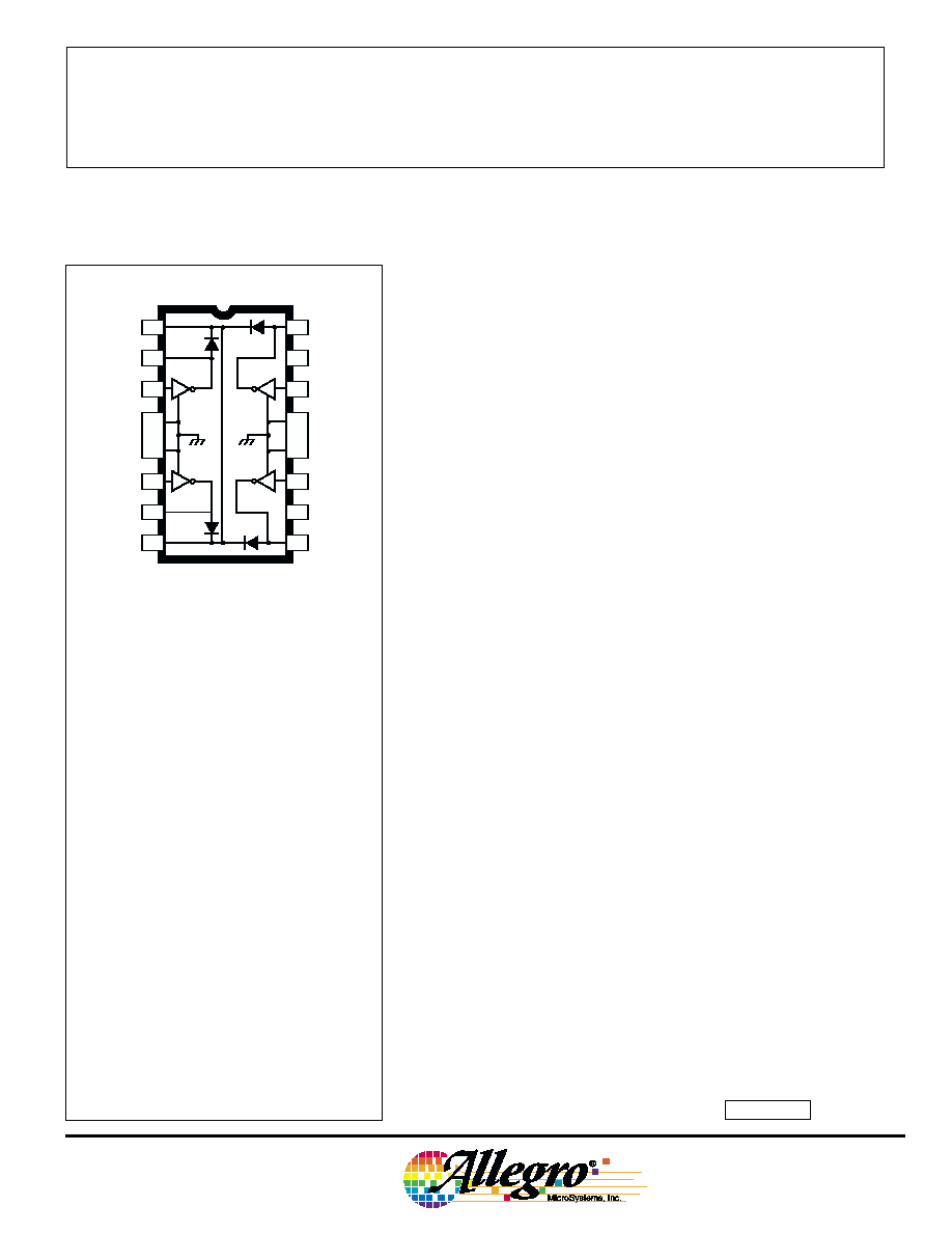
2064
THRU
2069
ULN2064/65B
K
16
15
14
13
12
6
11
7
10
8
9
1
2
3
4
5
Dwg. No. A-9765A
B
C
K
C
B
GND
GND
C
NC
B
GND
GND
B
NC
C

2064
THRU
2069
QUAD 1.5 A DARLINGTON
SWITCHES
115 Northeast Cutoff, Box 15036
Worcester, Massachusetts 01615-0036 (508) 853-5000
2
Part
Max.
Min.
Max.
Number*
V
CEX
V
CE(SUS)
V
IN
Application
ULN2064B
50 V
35 V
15 V
TTL, DTL, Schottky TTL,
ULN2064LB
and 5 V CMOS
ULN2065B
80 V
50 V
15 V
ULN2065LB
ULN2068B
50 V
35 V
15 V
TTL, DTL, Schottky TTL,
ULN2068LB
and 5 V CMOS
ULN2069B
80 V
50 V
15 V
ULN2069LB
SELECTION GUIDE
TEST FIGURES
FIGURE 8
FIGURE 7
FIGURE 6
FIGURE 5
Dwg. No. A-9736
Dwg. No. A-10,351
OPEN
IC
mA
VIN
VS
IS
V
Dwg. No. A-9734A
OPEN
VCE
V
VIN
IC
Dwg. No. A-9735A
FIGURE 4
FIGURE 1
Dwg. No. A-10,349
FIGURE 3
Dwg. No. A-9729A
Dwg. No. A-10,350
FIGURE 2
VCE
VIN
OPEN
IC
V
IB
OPEN
VCE
V
IC
Dwg. No. A-9732A
VIN
OPEN
mA
OPEN
IIN
IF
OPEN
VF
V
OPEN
VR
IR
µA
OPEN
OPEN
VCE
ICEX
µA
50
75
100
125
150
5
1
0
ALLOWABLE PACKAGE POWER DISSIPATION IN WATTS
TEMPERATURE IN
∞C
4
3
2
25
Dwg. GP-049-3
R = 6.0
∞C/W
JT
SUFFIX 'B', R = 43
∞C/W
JA
SUFFIX 'LB', R = 60
∞C/W
JA
Copyright © 1977, 2000 Allegro MicroSystems, Inc.
* Suffix `B' is a 16-pin DIP; `LB' is a 20-lead SOIC.

2064
THRU
2069
QUAD 1.5 A DARLINGTON
SWITCHES
www.allegromicro.com
3
Test
Applicable
Limits
Characteristic
Symbol
Fig.
Devices
Test Conditions
Min.
Max.
Units
Output Leakage Current
I
CEX
1
ULN2064B/LB
V
CE
= 50 V
--
100
µA
V
CE
= 50 V, T
A
= 70
∞C
--
500
µA
ULN2065B/LB
V
CE
= 80 V
--
100
µA
V
CE
= 80 V, T
A
= 70
∞C
--
500
µA
Output Sustaining Voltage
V
CE(SUS )
2
ULN2064B/LB
I
C
= 100 mA, V
IN
= 0.4 V
35
--
V
ULN2065B/LB
I
C
= 100 mA, V
IN
= 0.4 V
50
--
V
V
CE(SAT)
3
All
I
C
= 500 mA, I
B
= 625
µA
--
1.1
V
I
C
= 750 mA, I
B
= 935
µA
--
1.2
V
I
C
= 1.0 A, I
B
= 1.25 mA
--
1.3
V
l
C
= 1.25 A, I
B
= 2.0 mA
--
1.4
V
ULN2065B/LB
I
C
= 1.5 A, I
B
= 2.25 mA
--
1.5
V
Input Current
I
IN(ON)
4
All
V
IN
= 2.4 V
1.4
4.3
mA
V
IN
= 3.75 V
3.3
9.6
mA
Input Voltage
V
IN(ON)
5
All
V
CE
= 2.0 V, I
C
= 1.0 A
--
2.0
V
ULN2064B/LB
V
CE
= 2.0 V, I
C
= 1.25 A
--
2.5
V
ULN2065B/LB
V
CE
= 2.0 V, I
C
= 1.5 A
--
2.5
V
Turn-On Delay
t
PLH
--
All
0.5 E
in
to 0.5 E
out
--
1.0
µs
Turn-Off Delay
t
PHL
--
All
0.5 E
in
to 0.5 E
out
--
1.5
µs
Clamp Diode Leakage Current
I
R
6
ULN2064B/LB
V
R
= 50 V
--
50
µA
V
R
= 50 V, T
A
= 70
∞C
--
100
µA
ULN2065B/LB
V
R
= 80 V
--
50
µA
V
R
= 80 V, T
A
= 70
∞C
--
100
µA
Clamp Diode Forward Voltage
V
F
7
All
I
F
= 1.0 A
--
1.75
V
I
F
= 1.5 A
--
2.0
V
Collector-Emitter
Saturation Voltage
ELECTRICAL CHARACTERISTICS at +25
∞
C (unless otherwise noted).
Dwg. No. A-10,353C
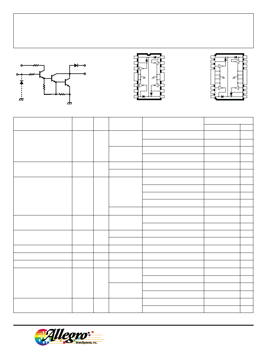
PARTIAL SCHEMATIC
K
7.2K
3K
350
C
B
K
16
15
14
13
12
6
11
7
10
8
9
1
2
3
4
5
B
C
K
C
B
GND
GND
C
NC
B
GND
GND
B
NC
C
Dwg. No. A-9765A
ULN2064/65B
Dwg. No. A-14,326
K
20
19
18
16
15
8
13
9
12
10
11
1
2
3
5
6
B
C
K
C
B
GND
GND
C
NC
B
GND
GND
B
NC
C
14
7
17
4
GND
GND
GND
GND
ULN2064/65LB
2064
THRU
2069
QUAD 1.5 A DARLINGTON
SWITCHES
115 Northeast Cutoff, Box 15036
Worcester, Massachusetts 01615-0036 (508) 853-5000
4
PARTIAL SCHEMATIC
Test
Applicable
Limits
Characteristic
Symbol
Fig.
Devices
Test Conditions
Min.
Max.
Units
Output Leakage Current
I
CEX
1
ULN2068B/LB
V
CE
= 50 V
--
100
µA
V
CE
= 50 V, T
A
= 70
∞C
--
500
µA
ULN2069B/LB
V
CE
= 80 V
--
100
µA
V
CE
= 80 V, T
A
= 70
∞C
--
500
µA
Output Sustaining Voltage
V
CE(SUS )
2
ULN2068B/LB
I
C
= 100 mA, V
IN
= 0.4 V
35
--
V
ULN2069B/LB
I
C
= 100 mA, V
IN
= 0.4 V
50
--
V
V
CE(SAT)
3
All
I
C
= 500 mA, V
IN
= 2.75 V
--
1.1
V
I
C
= 750 mA, V
IN
= 2.75 V
--
1.2
V
I
C
= 1.0 A, V
IN
= 2.75 V
--
1.3
V
l
C
= 1.25 A, V
IN
= 2.75 V
--
1.4
V
ULN2069B/LB
I
C
= 1.5 A, V
IN
= 2.75 V
--
1.5
V
Input Current
I
IN(ON)
4
All
V
IN
= 2.75 V
--
550
µA
V
IN
= 3.75 V
--
1000
µA
Input Voltage
V
IN(ON)
5
ULN2068B/LB
V
CE
= 2.0 V, I
C
= 1.25 A
--
2.75
V
ULN2069B
V
CE
= 2.0 V, I
C
= 1.5 A
--
2.75
V
Supply Current
I
S
8
All
I
C
= 500 mA, V
IN
= 2.75 V
--
6.0
mA
Turn-On Delay
t
PLH
--
All
0.5 E
in
to 0.5 E
out
--
1.0
µs
Turn-Off Delay
t
PHL
--
All
0.5 E
in
to 0.5 E
out
,
I
C
= 1.25 A
--
1.5
µs
Clamp Diode Leakage Current
I
R
6
ULN2068B/LB
V
R
= 50 V
--
50
µA
V
R
= 50 V, T
A
= 70
∞C
--
100
µA
ULN2069B/LB
V
R
= 80 V
--
50
µA
V
R
= 80 V, T
A
= 70
∞C
--
100
µA
Clamp Diode Forward Voltage
V
F
7
All
I
F
= 1.0 A
--
1.75
V
I
F
= 1.5 A
--
2.0
V
Collector-Emitter
Saturation Voltage
ELECTRICAL CHARACTERISTICS at +25
∞
C, V
S
= 5.0 V (unless otherwise noted).
Dwg. No. A-10,354C
K
7.2K
3K
2.5K
C
B
900
VS
K
16
15
14
13
12
6
11
7
10
8
9
1
2
3
4
5
B
NC
C
C
B
GND
GND
C
B
VS
GND
GND
B
C
K
Dwg. No. A-10,310
ULN2068/69B
K
20
19
18
16
15
8
13
9
12
10
11
1
2
3
5
6
B
NC
C
C
B
GND
GND
C
B
VS
GND
GND
B
C
K
14
7
17
4
GND
GND
GND
GND
ULN2068/69LB
Dwg. No. A-14,327

2064
THRU
2069
QUAD 1.5 A DARLINGTON
SWITCHES
www.allegromicro.com
5
PEAK COLLECTOR CURRENT AS A FUNCTION OF DUTY CYCLE
(Dual in-line packaged devices)
1.5
1.0
0.5
0
0
ALLOW
ABLE PEAK COLLECTOR CURRENT IN AMPERES at 50
∞
C
20
40
60
80
100
PERCENT DUTY CYCLE
4
3
2
NUMBER OF OUTPUTS CONDUCTING
SIMULTANEOUSLY
ULN2064B THROUGH ULN2069B
WITH STAVER V-7 HEAT SINK
27.5
∞C/W
Dwg. No. A-10,398C
1.5
1.0
0.5
0
0
ALLOW
ABLE PEAK COLLECTOR CURRENT IN AMPERES at 70
∞
C
20
40
60
80
100
PERCENT DUTY CYCLE
4
3
2
1
NUMBER OF OUTPUTS CONDUCTING
SIMULTANEOUSLY
ULN2064B THROUGH ULN2069B
Dwg. No. A-10,360B
1.5
1.0
0.5
0
0
ALLOW
ABLE PEAK COLLECTOR CURRENT IN AMPERES at 50
∞
C
20
40
60
80
100
PERCENT DUTY CYCLE
4
3
2
NUMBER OF OUTPUTS CONDUCTING
SIMULTANEOUSLY
ULN2064B THROUGH ULN2069B
Dwg. No. A-10,361B
1.5
1.0
0.5
0
0
ALLOW
ABLE PEAK COLLECTOR CURRENT IN AMPERES at 50
∞
C
20
40
60
80
100
PERCENT DUTY CYCLE
4
3
2
NUMBER OF OUTPUTS CONDUCTING
SIMULTANEOUSLY
ULN2064B THROUGH ULN2069B
WITH STAVER V-8 HEAT SINK
37.5
∞C/W
Dwg. No. A-10,400C