 | –≠–ª–µ–∫—Ç—Ä–æ–Ω–Ω—ã–π –∫–æ–º–ø–æ–Ω–µ–Ω—Ç: 3134 | –°–∫–∞—á–∞—Ç—å:  PDF PDF  ZIP ZIP |
Always order by complete part number, e.g., A3134ELT .
FEATURES
s Superior Temperature Stability
s Operation From Unregulated Supply
s Open-Collector 25 mA Output
s Reverse Battery Protection
s Activate With Small, Commercially Available Permanent Magnets
s Solid-State Reliability
s Small Size
s Resistant to Physical Stress
This low-hysteresis bipolar Hall-effect switch is an extremely
temperature-stable and stress-resistant sensor especially suited for
operation over extended temperature ranges to +150
∞
C. Superior
high-temperature performance is made possible through a novel Schmitt
trigger circuit that maintains operate and release point stability by
compensating for temperature changes in the Hall element. Additionally,
internal compensation provides magnetic switch points that become more
sensitive with temperature, hence offsetting the usual degradation of the
magnetic field with temperature. Its low hysteresis makes this device
ideal for detecting small changes in magnetic field strength or for use
with inexpensive magnets.
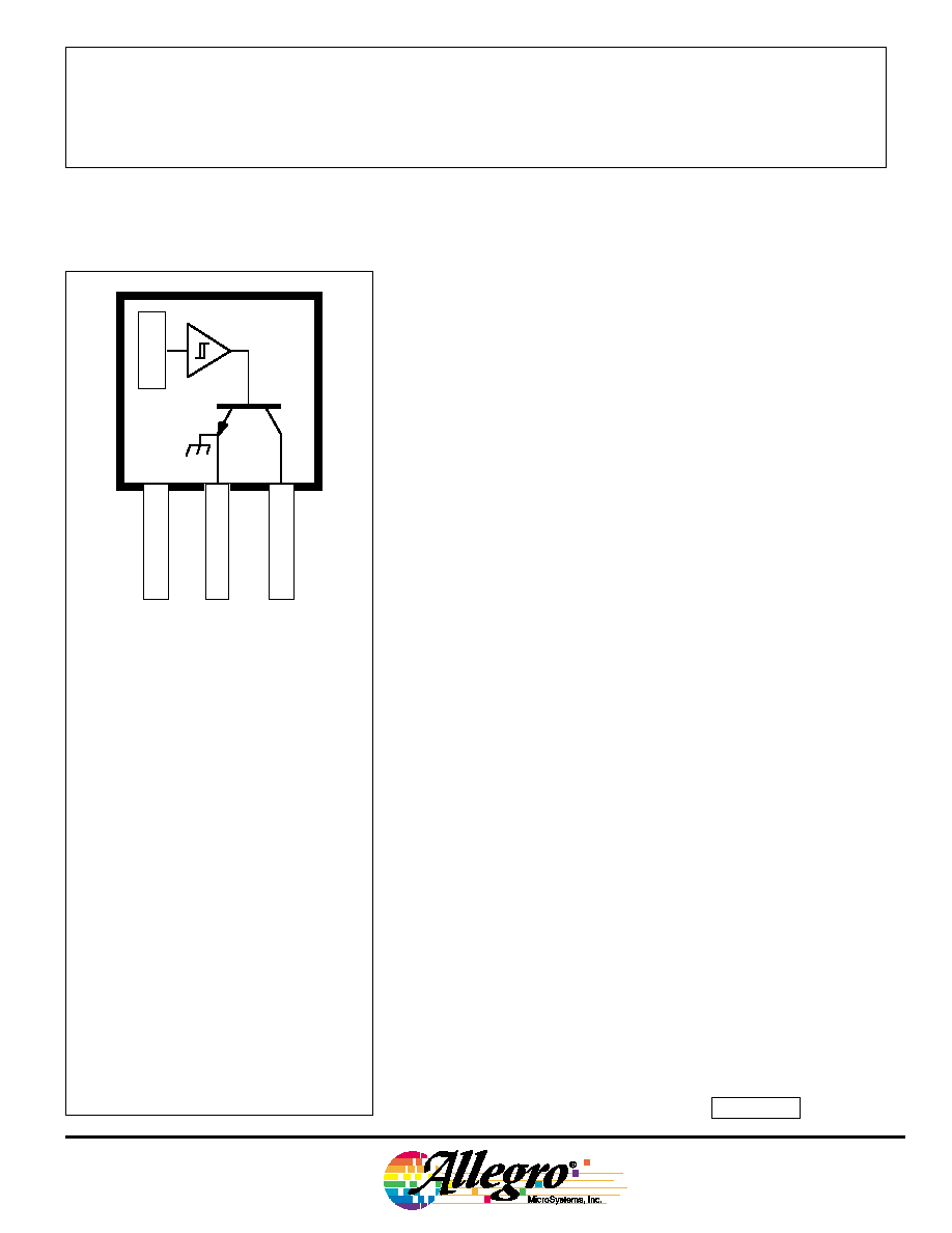
The device includes on a single silicon chip a voltage regulator,
quadratic Hall-voltage generator, temperature compensation circuit,
signal amplifier, Schmitt trigger, and a buffered open-collector output to
sink up to 25 mA. The on-board regulator permits operation with supply
voltages of 4.5 volts to 24 volts.
The first character of the part number suffix determines the device
operating temperature range. Suffix `E≠' is for -40
∞
C to +85
∞
C, and
suffix `L≠' is -40
∞
C to +150
∞
C. Two package styles provide a magneti-
cally optimized package for most applications. Suffix `≠LT' is a minia-
ture SOT89/TO-243AA transistor package for surface-mount applica-
tions while suffix `≠UA' is a three-lead ultra-mini-SIP.
Pinning is shown viewed from branded side.
ABSOLUTE MAXIMUM RATINGS
at T
A
= +25
∞
C
Supply Voltage, V
CC
............................. 30 V
Reverse Battery Voltage, V
RCC
.......... -30 V
Magnetic Flux Density, B .......... Unlimited
Output OFF Voltage, V
OUT
.................. 30 V
Reverse Output Voltage, V
OUT
........... -0.5 V
Continuous Output Current,
I
OUT
............................................ 25 mA
Operating Temperature Range, T
A
Suffix `E≠' .................. -40
∞
C to +85
∞
C
Suffix `L≠' ................ -40
∞
C to +150
∞
C
Storage Temperature Range,
T
S
.............................. -65
∞
C to +170
∞
C
Data Sheet
27631.4D
3134
BIPOLAR HALL-EFFECT SWITCH
FOR HIGH-TEMPERATURE OPERATION
Dwg. PH-003A
1
SUPPLY
V
CC
GROUND
3
2
OUTPUT
X

3134
LOW-HYSTERESIS
BIPOLAR HALL-EFFECT SWITCH
FOR HIGH-TEMP. OPERATION
115 Northeast Cutoff, Box 15036
Worcester, Massachusetts 01615-0036 (508) 853-5000
Limits
Characteristic
Symbol
Test Conditions
Min.
Typ.
Max.
Units
Supply Voltage
V
CC
Operating
4.5
--
24
V
Output Saturation Voltage
V
OUT(SAT)
I
OUT
= 20 mA, B > B
OP
--
175
400
mV
Output Leakage Current
I
OFF
V
OUT
= 24 V, B < B
RP
--
0.05
1.0
µ
A
Supply Current
I
CC
B < B
RP
(Output OFF)
--
3.2
9.0mA
B > B
OP
(Output ON)
--
5.0--
mA
Output Rise Time
t
r
R
L
= 820
, C
L
= 20 pF
--
100
--
ns
Output Fall Time
t
f
R
L
= 820
, C
L
= 20 pF
--
100
--
ns
ELECTRICAL CHARACTERISTICS over operating temperature range, at V
CC
= 12 V.
MAGNETIC CHARACTERISTICS over oper. temp. and oper. supply voltage ranges.
V
CC
X
REG.
Dwg. FH-005-3
GROUND
OUTPUT
1
3
2
FUNCTIONAL BLOCK DIAGRAM
Limits
Characteristic
Symbol
Test Conditions
Min.
Typ.
Max.
Units
Operate Point
B
OP
-408.5
60 G
Release Point
B
RP
-50-19
50 G
Hysteresis
B
hys
5.027
55
G
Copyright © 1995, 2003 Allegro MicroSystems, Inc.
NOTES: B
OP
= operate point (output turns ON); B
RP
= release point (output turns OFF); B
hys
= hysteresis (B
OP
- B
RP
).
As used here, negative flux densities are defined as less than zero (algebraic convention).
Typical values are at T
A
= +25
∞
C and V
CC
= 12 V.
1 gauss (G) is exactly equal to 0.1 millitesla (mT).

3134
LOW-HYSTERESIS
BIPOLAR HALL-EFFECT SWITCH
FOR HIGH-TEMP. OPERATION
www.allegromicro.com
TYPICAL OPERATING CHARACTERISTICS
0
25
50
75
100
AMBIENT TEMPERATURE IN
∞
∞
∞
∞
C
-50
Dwg. GH-053
125
-25
SUPPLY CURRENT IN mA
5.0
4.0
3.0
2.0
1.0
150
V = 12 V
CC
B < B
RP
V = 24 V
CC
V = 4.5 V
CC
OUTPUT SATURATION VOLTAGE
SUPPLY CURRENT
0
25
50
75
100
AMBIENT TEMPERATURE IN
∞
∞
∞
∞
C
-50
Dwg. GH-052
125
-25
SWITCH POINT IN GAUSS
40
20
0
-20
-40
RELEASE POINT
OPERATE POINT
150
CC
V = 4.5 V≠24 V
SWITCH POINTS
HYSTERESIS
0
25
50
75
100
AMBIENT TEMPERATURE IN
∞
∞
∞
∞
C
-50
Dwg. GH-051
125
-25
HYSTERESIS IN GAUSS
20
10
0
150
30
CC
V = 4.5 V≠24 V
40
50
0
25
50
75
100
300
0
AMBIENT TEMPERATURE IN
∞
∞
∞
∞
C
200
100
-50
Dwg. GH-029
SATURATION VOLTAGE IN mV
150
-25
125
I = 20 mA
V = 4.5≠24 V
OUT
CC
3134
LOW-HYSTERESIS
BIPOLAR HALL-EFFECT SWITCH
FOR HIGH-TEMP. OPERATION
115 Northeast Cutoff, Box 15036
Worcester, Massachusetts 01615-0036 (508) 853-5000
APPLICATIONS INFORMATION
Extensive applications information for Hall-effect sensors is available in:
∑ Hall-Effect IC Applications Guide, Application Note 27701;
∑ Hall-Effect Devices: Soldering, Gluing, Potting, Encapsulating, and Lead
Forming, Application Note 27703.1;
∑ Soldering of Through-Hole Hall-Sensor Dervices, Application Note 27703;
and
∑ Soldering of Surface-Mount Hall-Sensor Devices, Application Note 27703.2.
All are provided in Allegro Electronic Data Book, AMS-702. or at
www.allegromicro.com
OPERATION
The output of these devices (pin 3) switches low when the magnetic field
at the Hall sensor exceeds the operate point threshold (B
OP
). At this point, the
output voltage is V
OUT(SAT)
. When the magnetic field is reduced to below the
release point (B
RP
) the device output goes high. Note especially that release
can occur when the magnetic field is removed but to ensure release, a field
reversal is required. The difference in the magnetic operate and release points
is called the hysteresis (B
hys
) of the device. This built-in hysteresis allows
clean switching of the output even in the presence of external mechanical
vibration and electrical noise.
Powering up the device in the absence of a magnetic field (less than B
OP
and higher than B
RP
) will allow in indeterminate output state. The correct state
is warranted after the first excursion beyond B
OP
or B
RP
.
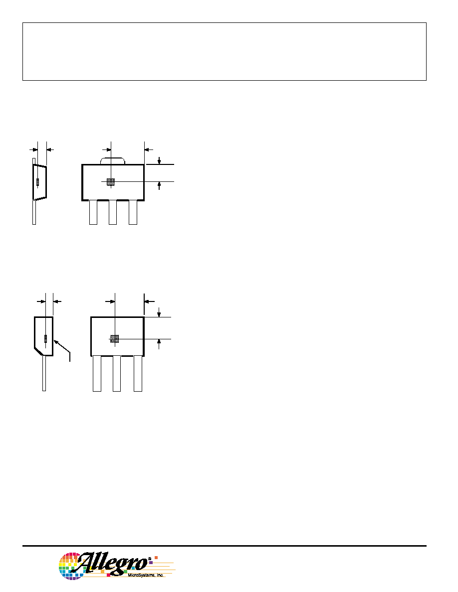
Suffix "UA"
SENSOR LOCATIONS
(
±
0.005" [0.13 mm] die placement)
1
3
2
Dwg. MH-011-4C
0.0195"
0.50 mm
NOM
BRANDED
SURFACE
ACTIVE AREA DEPTH
0.083"
2.10 mm
0.060"
1.51 mm
A
Suffix "LT"
1
3
2
Dwg. MH-008-4C
0.0305"
0.775 mm
NOM
ACTIVE AREA DEPTH
0.050"
1.27 mm
0.090"
2.27 mm
A
The products described herein are manufactured under one or more of the following
U.S. patents: 5,045,920; 5,264,783; 5,442,283; 5,389,889; 5,581,179; 5,517,112;
5,619,137; 5,621,319; 5,650,719; 5,686,894; 5,694,038; 5,729,130; 5,917,320; and
other patents pending.
Allegro MicroSystems, Inc. reserves the right to make, from time to time, such
departures from the detail specifications as may be required to permit improvements in
the performance, reliability, or manufacturability of its products. Before placing an
order, the user is cautioned to verify that the information being relied upon is current.
Allegro products are not authorized for use as critical components in life-support
appliances, devices, or systems without express written approval.
The information included herein is believed to be accurate and reliable. However,
Allegro MicroSystems, Inc. assumes no responsibility for its use; nor for any infringe-
ments of patents or other rights of third parties that may result from its use.
3134
LOW-HYSTERESIS
BIPOLAR HALL-EFFECT SWITCH
FOR HIGH-TEMP. OPERATION
www.allegromicro.com
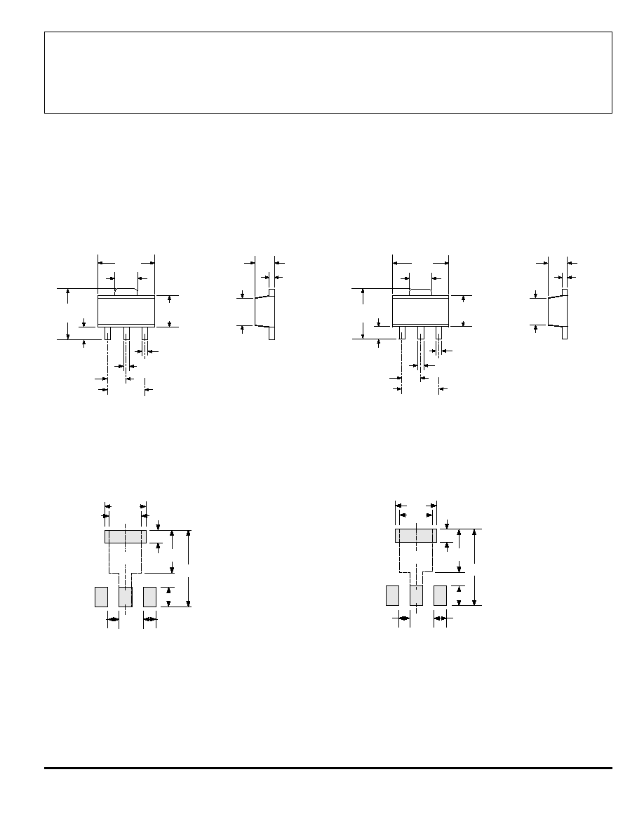
PACKAGE DESIGNATOR `LT'
(SOT89/TO-243AA)
Dimensions in Inches
(for reference only)
Dimensions in Millimeters
(controlling dimensions)
NOTES: 1.
Exact body and lead configuration at vendor's option within limits shown.
2.
Supplied in bulk pack (500 pieces per bag) or add "TR" to part number for tape and reel.
3.
Only low-temperature (
240
∞
C) reflow-soldering techniques are recommended for SOT89 devices.
Dwg. MA-009-3A in
1
2
3
0.072
0.064
0.167
0.155
0.059
BSC
0.0189
0.0142
0.047
0.035
0.102
0.090
0.063
0.055
0.0173
0.0138
0.090
0.084
0.0221
0.0173
0.118
BSC
0.181
0.173
Dwg. MA-009-3A mm
1
2
3
4.60
4.40
1.83
1.62
4.25
3.94
1.50
BSC
0.48
0.36
1.20
0.89
2.60
2.29
1.60
1.40
0.44
0.35
2.29
2.13
0.56
0.44
3.00
BSC
1
B
0.098
0.031
0.102
0.047
0.181
0.079
Dwg. MA-012-3 in
Pads 1, 2, 3, and A -- Standard SOT89 Layout
Pads 1, 2, 3, and B -- Low-Stress Version
Pads 1, 2, and 3 only -- Lowest Stress, But Not Self Aligning
2
0.028
TYP
0.031
TYP
A
3
1
3
B
2.5
0.8
2.6
1.2
4.6
2.0
Dwg. MA-012-3 mm
Pads 1, 2, 3, and A -- Standard SOT89 Layout
Pads 1, 2, 3, and B -- Low-Stress Version
Pads 1, 2, and 3 only -- Lowest Stress, But Not Self Aligning
2
0.7
TYP
0.8
TYP
A