 | –≠–ª–µ–∫—Ç—Ä–æ–Ω–Ω—ã–π –∫–æ–º–ø–æ–Ω–µ–Ω—Ç: 3195 | –°–∫–∞—á–∞—Ç—å:  PDF PDF  ZIP ZIP |
3195
PROTECTED, HIGH-TEMP.,
ACTIVE PULL-DOWN
HALL-EFFECT LATCH
3195
PROTECTED, HIGH-TEMPERATURE,
HALL-EFFECT LATCH WITH ACTIVE PULL-DOWN
Always order by complete part number, e.g., A3195LU .
These Hall-effect latches are capable of sensing magnetic fields
while using an unprotected power supply. The A3195≠ can provide
position and speed information by providing a digital output for mag-
netic fields that exceed their predefined switch points. These devices
operate down to zero speed and have switch points that are designed
to be extremely stable over a wide operating temperature and voltage
range. The latching characteristics make them ideal for use in pulse
counting applications when used with a multi-pole ring magnet.
A 25 mA high-side driver combined with an active pull-down is espe-
cially useful for driving capacitive loads. Output short-circuit protection
allows for an increased wiring harness fault tolerance. The tempera-
ture compensated switch points, the wide operating voltage range, and
the integrated protection make these devices ideal for use in automo-
tive applications such as transmission speed sensors and integrated
wheel bearing speed sensors.
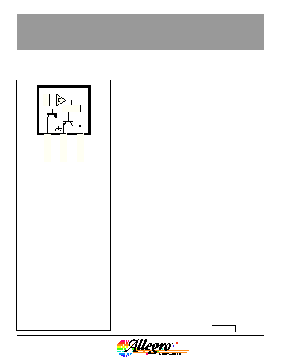
Each monolithic device contains an integrated Hall-effect trans-
ducer, a temperature-compensated comparator, a voltage regulator,
and a buffered high-side driver with an active pull-down. Supply
protection is made possible by the integration of overvoltage shutdown
circuitry that monitors supply fault conditions. Output protection
circuitry includes source and sink current current limiting for short
circuits to supply or ground.
The A3195E≠ is rated for operation over a temperature range of
-40
∞
C to +85
∞
C; the A3195L≠ is rated for operation over an extended
temperature range of -40
∞
C to +150
∞
C. They are supplied in a three-
lead SIP (suffix ≠U) or a surface-mount SOT-89 (suffix ≠LT).
FEATURES
s
Internal Protection For Automotive (ISO/DIN) Transients
s
Operation From Unregulated Supply
s
Reverse Battery Protection
s
Undervoltage Lockout
s
Supply Noise-Suppression Circuitry
s
Output Short-Circuit Protection
s
Output Zener Clamp
s
Thermal Protection
s
Symmetrical Latching Switch Points
s
Operable with Multipole Ring Magnets
Dwg. PH-013
1
SUPPLY
V
CC
GROUND
3
2
OUTPUT
X
LATCH
ABSOLUTE MAXIMUM RATINGS
Supply Voltage, V
CC
(100 ms) .......... 115 V*
(continuous) ................................... 26 V
Reverse Battery Voltage,
V
RCC
(100 ms) ............................ -100 V
(continuous) ................................. -30 V
Magnetic Flux Density, B ........... Unlimited
Reverse Output Voltage, V
OUT
......... -0.5 V
Continuous Output Current,
I
OUT
........................... Internally Limited
Package Power Dissipation,
P
D
........................................ See Graph
Junction Temperature, T
J
................. 170
∞
C
Operating Temperature Range, T
A
Suffix "E≠" .................... -40
∞
C to +85
∞
C
Suffix "L≠" .................. -40
∞
C to +150
∞
C
Storage Temperature, T
S
................. 170
∞
C
*Fault condition, internal overvoltage shutdown
above 28 V.
Data Sheet
27609.15*
Pinning is shown viewed from branded side.
3195
PROTECTED, HIGH-TEMP.,
ACTIVE PULL-DOWN
HALL-EFFECT LATCH
115 Northeast Cutoff, Box 15036
Worcester, Massachusetts 01615-0036 (508) 853-5000
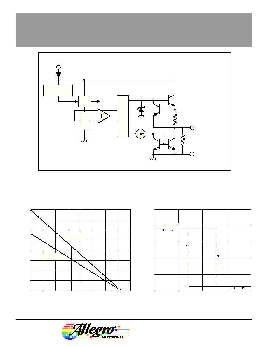
FUNCTIONAL BLOCK DIAGRAM
REG.
OUTPUT
3
GROUND
2
X
Dwg. FH-013
V
CC
1
CURRENT
LIMIT
15k
OVERVOLT.
LOCKOUT
LATCH
26 V
MAX
0
+B
0
OUTPUT VOLTAGE IN VOLTS
FLUX DENSITY
Dwg. GH-034-3
-B
RP
B
V
OUT(L)
V
OUT(H)
OP
B
TRANSFER CHARACTERISTICS
600
400
200
40
80
120
160
0
AMBIENT TEMPERATURE IN
∞
C
ALLOWABLE PACKAGE POWER DISSIPATION IN mW
Dwg. GH-054A
"U" PACKAGE
R
JA
= 183
∞
C/W
"LT" PACKAGE
R
JA
= 258
∞
C/W
60
100
140
180
700
500
300
100
20
800
W
Copyright © 1995, 1997, Allegro MicroSystems, Inc.

3195
PROTECTED, HIGH-TEMP.,
ACTIVE PULL-DOWN
HALL-EFFECT LATCH
ELECTRICAL CHARACTERISTICS
over operating voltage and temperature range (unless otherwise specified).
Limits
Characteristic
Symbol
Test Conditions
Min.
Typ.
Max.
Units
Supply Voltage
V
CC
Operating (but V
CC
x I
CC
VS
T
A
limited)
3.8
12
26
V
Overvoltage Shutdown*
V
CC(OV)
B > B
OP
28
--
55
V
Output Voltage, High
V
OUT(H)
B < B
RP,
I
OUT
= -20 mA
V
CC
-2
--
V
CC
-0.3
V
(Source Voltage)
Output Voltage, Low
V
OUT(L)
B > B
OP,
I
OUT
<100
µ
A
--
0.1
0.2
V
(Sink Voltage)
B > B
OP,
I
OUT
= 5 mA
--
0.25
0.5
V
Output Clamp Voltage
V
OUT(CLMP)
B < B
RP
, V
CC
> 26 V,
I
OUT
= 0
15
18
21
V
Output Current Limit
I
OUTMAX
B < B
RP
, V
CC
= 12 V
-26
--
-70
mA
B > B
OP
, V
OUT
< 14 V
8.0
--
25
mA
Supply Current
I
CC
B < B
RP
, V
CC
= 18 V,
I
OUT
= 0
--
6.0
9.0
mA
B > B
OP
, V
CC
= 18 V, I
OUT
= 0
--
8.0
12
mA
V
CC
= +115 V*
--
8.0
17
mA
Reverse Battery Current*
I
RCC
V
RCC
= -35 V*
--
-0.1
-5.0
mA
V
RCC
= -100 V*
--
-0.1
-10
mA
Output Rise Time
t
r
C
L
= 20 pF, R
L
= 330
--
0.12
2.0
µ
s
Output Fall Time
t
f
C
L
= 20 pF, R
L
= 330
--
0.30
5.0
µ
s
Package Thermal Resist.
R
JA
"LT" Package
--
258
--
∞
C/W
"U" Package
--
183
--
∞
C/W
MAGNETIC CHARACTERISTICS
over operating voltage range (unless otherwise specified).
Limits
Characteristic
Symbol
Test Conditions
Min.
Typ.
Max.
Units
Operate Point
B
OP
T
A
= -40
∞
C
60
125
200
G
T
A
= +25
∞
C
50
110
160
G
T
A
= Maximum
40
100
150
G
Release Point
B
RP
T
A
= -40
∞
C
-200
-125
-60
G
T
A
= +25
∞
C
-160
-110
-50
G
T
A
= Maximum
-150
-100
-40
G
Hysteresis
B
hys
T
A
= -40
∞
C
150
250
--
G
(B
OP
- B
RP
)
T
A
= +25
∞
C
130
220
--
G
T
A
= Maximum
110
200
--
G
NOTES: Negative current is defined as coming out of (sourcing) the output.
B
OP
= magnetic operate point (output turns ON); B
RP
= magnetic release point (output turns OFF).
As used here, negative flux densities are defined as less than zero (algebraic convention).
Typical values are at T
A
= +25
∞
C and V
CC
= 12 V.
* Fault condition. Device is shut down and operation is not possible.
3195
PROTECTED, HIGH-TEMP.,
ACTIVE PULL-DOWN
HALL-EFFECT LATCH
115 Northeast Cutoff, Box 15036
Worcester, Massachusetts 01615-0036 (508) 853-5000
TYPICAL OPERATING CHARACTERISTICS
0
25
50
75
100
AMBIENT TEMPERATURE IN
∞
C
-50
Dwg. GH-004-1
125
-25
20
0
-20
-40
-60
OUTPUT LOW,
(SINKING CURRENT)
B
B
OP
OUTPUT HIGH,
(SOURCING CURRENT)
B
B
RP
150
CC
V = 16 V
CURRENT LIMIT IN mA
0
25
50
75
100
AMBIENT TEMPERATURE IN
∞
C
-50
Dwg. GH-052-1
125
-25
SWITCH POINTS IN GAUSS
200
100
0
-100
-200
RELEASE POINT
OPERATE POINT
150
CC
V = 3.8 V≠26 V
9.0
SUPPLY CURRENT IN mA
8.0
7.0
6.0
5.0
0
25
50
75
100
AMBIENT TEMPERATURE IN
∞
C
-50
Dwg. GH-028-2
125
-25
V = 26 V
CC
150
V = 12 V
CC
V = 3.8 V
CC
OUTPUT HIGH, B
B
OP
OUTPUT LOW, B
B
RP
0
25
50
75
100
Vcc
0
AMBIENT TEMPERATURE IN
∞
C
Vcc - 1
0.4
-50
Dwg. GH-040-2
OUTPUT VOLTAGE IN VOLTS
150
-25
125
Vcc - 2
0.2
OUTPUT LOW,
(SINKING CURRENT)
B
B
OP
OUTPUT HIGH,
(SOURCING CURRENT)
B
B
CC
V = 16 V
I = 5 mA
OUT
I
100
µ
A
OUT
I = -20 mA
RP
OUT
TYPICAL OPERATING CHARACTERISTICS
Output Current Limit
3195
PROTECTED, HIGH-TEMP.,
ACTIVE PULL-DOWN
HALL-EFFECT LATCH
OPERATION
In operation, the output transistor is OFF
until the strength of the magnetic field
perpendicular to the surface of the chip
exceeds the threshold or operate point (B
OP
).
When the field strength exceeds B
OP
, the
output transistor switches ON (a logic low)
and is capable of sinking 35 mA of current.
The output transistor switches OFF (a
logic high) when magnetic field reversal
results in a magnetic flux density below the
OFF threshold (B
RP
). This is illustrated in the
transfer characteristics graph. Note that the
device latches; that is, a south pole of
sufficient strength will turn the device ON.
Removal of the south pole will leave the
device ON. The presence of a north pole of
sufficient strength is required to turn the
device OFF.
The switch points increase in sensitivity
with increasing temperature to compensate
for the typical ferrite magnet temperature
characteristic. The simplest form of magnet
that will operate these devices is a ring
magnet. Other methods of operation are
possible.
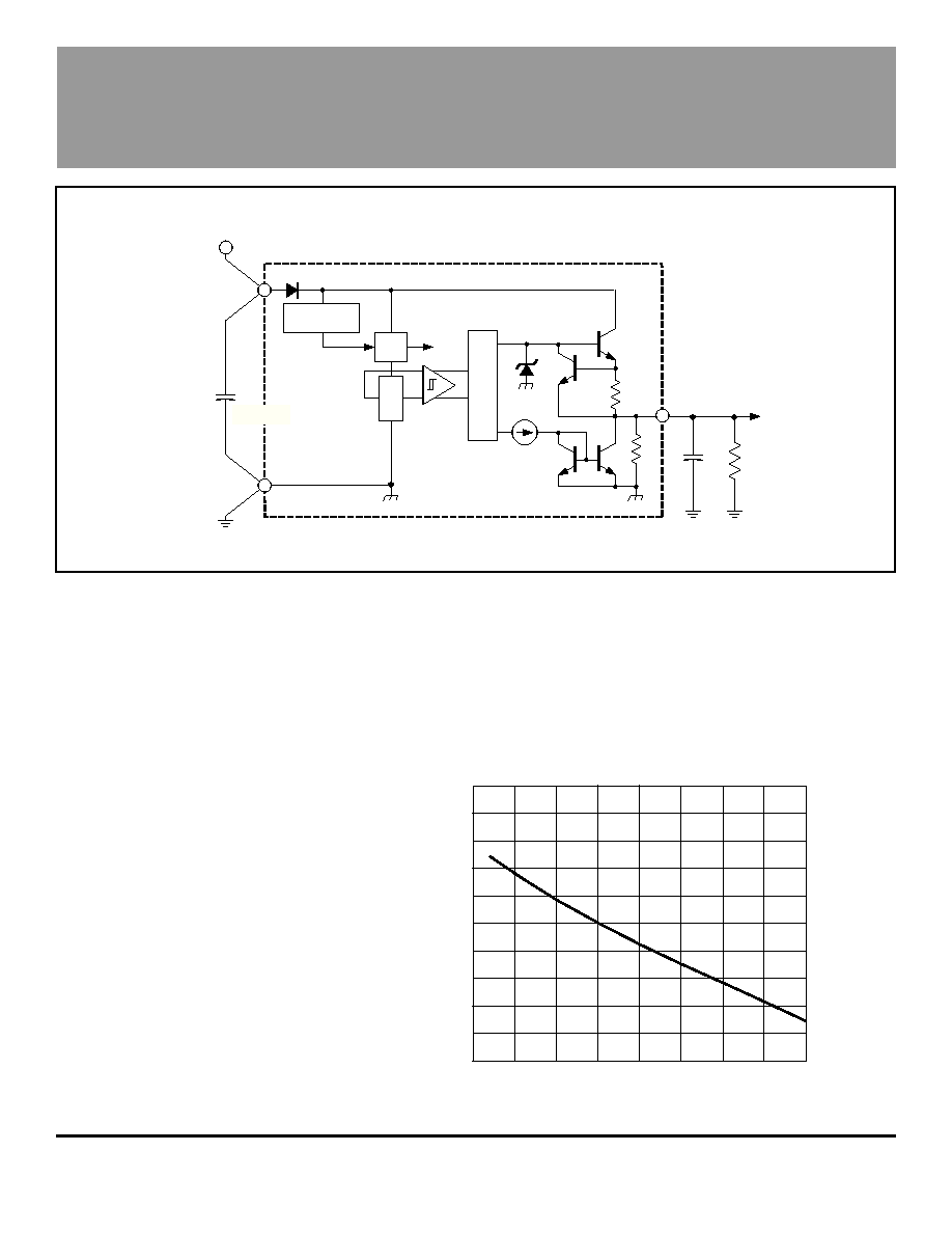
TEST CIRCUIT AND
TYPICAL APPLICATION
An external 0.1
µ
F to 0.47
µ
F capacitor, with good high-frequency
characteristics, should be connected between terminals 1 and 2 to
bypass high-voltage noise and reduce EMI susceptibility.
Internal Pull-Down Resistor. An internal pull-down resistor
(nominal 15 k
) is provided to allow testing of the device without the
need for an external load.
3.8 V TO 26 V
WITH TRANSIENTS
V
CC
Dwg. EH-007
L
R
TO
µ
P
L
C
3
X
BYPASS
C
2
1
0
25
50
75
100
20
10
AMBIENT TEMPERATURE IN
∞
C
18
14
-50
Dwg. GH-060
PULL-DOWN RESISTANCE IN k
150
-25
125
16
12