 | –≠–ª–µ–∫—Ç—Ä–æ–Ω–Ω—ã–π –∫–æ–º–ø–æ–Ω–µ–Ω—Ç: 3961 | –°–∫–∞—á–∞—Ç—å:  PDF PDF  ZIP ZIP |
3961
DUAL FULL-BRIDGE
PWM MOTOR DRIVER
DISCONTINUED PRODUCT
--
FOR REFERENCE ONL
Y
E
SENSE
V
GROUND
GROUND
GROUND
REF
V
RC
GROUND
24
23
22
21
20
19
18
17
1
2
3
4
5
6
7
8
9
10
16
15
1
1
BB1
OUT
1
OUT
1B
OUT
2B
SENSE
OUT
2A
V
FULL/PD
I
RC
2
BB2
2
PHASE
ENABLE
11
12
1
1
14
13
PHASE
ENABLE
2
2
REF
V
IN
OUT
1A
E
2
V
CC
Designed for pulse-width modulated (PWM) current control of
bipolar stepper motors, the A3961S-- is capable of continuous output
currents to
±
800 mA and operating voltages to 45 V. Internal fixed
off-time PWM current-control circuitry can be used to regulate the
maximum load current to a desired value. An internal precision voltage
reference is provided to improve motor peak current control accuracy.
The peak load current limit is set by the user's selection of an external
resistor divider and current-sensing resistors.
The fixed off-time pulse duration is set by user-selected external
RC timing networks. The capacitor in the RC timing network also
determines a user-selectable blanking window that prevents false
triggering of the PWM current control circuitry during switching transi-
tions. This eliminates the need for two external RC filter networks on
the current-sensing comparator inputs.
For each bridge the PHASE input controls load current polarity by
selecting the appropriate source and sink driver pair. For each bridge
the ENABLE input, when held high, disables the output drivers. Special
power-up sequencing is not required. Internal circuit protection includes
thermal shutdown with hysteresis, transient-suppression diodes, and
crossover-current protection.
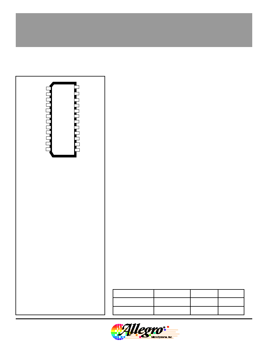
The A3961S-- is supplied in a choice of two power packages:
24-pin dual-in-line plastic package with copper heat-sink tabs and
24-lead plastic SOIC with copper heat-sink tabs. In both packages the
power tab is at ground potential and needs no electrical isolation.
FEATURES
s
±
800 mA Continuous Output Current Rating
s
45 V Output Voltage Rating
s
Internal PWM Current Control, Saturated Sink Drivers
s
Internally Generated Precision 2.5 V Reference
s
Internal Transient-Suppression Diodes
s
Internal Thermal-Shutdown Circuitry
s
Crossover-Current Protection, UVLO Protection
PART NUMBER
PACKAGE
R
JA
R
JT
A3961SB
24-Pin DIP
40
∞
C/W
6
∞
C/W
A3961SLB
24-Lead SOIC
55
∞
C/W
6
∞
C/W
Always order by complete part number:
DUAL FULL-BRIDGE PWM MOTOR DRIVER
Note the A3961SB (DIP) and the A3961SLB
(SOIC) are electrically identical and share a
common terminal number assignment.
ABSOLUTE MAXIMUM RATINGS
Load Supply Voltage, V
BB
. . . . . . . . . . 45 V
Output Current, I
OUT
. . . . . . . . . .
±
800 mA*
Logic Supply Voltage, V
CC
. . . . . . . . . 7.0 V
Logic Input Voltage Range,
V
IN
. . . . . . . . . . . -0.3 V to V
CC
+ 0.3 V
Sense Voltage, V
SENSE
. . . . . . . . . . . . 1.0 V
Reference Output Current,
I
REF OUT
. . . . . . . . . . . . . . . . . . . 1.0 mA
Package Power Dissipation,
P
D
. . . . . . . . . . . . . . . . . . . . See Graph
Operating Temperature Range,
T
A
. . . . . . . . . . . . . . . . . -20∞C to +85∞C
Junction Temperature, T
J
. . . . . . . +150∞C
Storage Temperature Range,
T
S
. . . . . . . . . . . . . . . . -55∞C to +150∞C
* Output current rating may be limited by duty
cycle, ambient temperature, and heat sinking.
Under any set of conditions, do not exceed the
specified current rating or a junction tempera-
ture of 150∞C.
Fault conditions that produce excessive
junction temperature will activate device
thermal shutdown circuitry. These conditions
can be tolerated but should be avoided.
Data Sheet
29319.26
3961
3961
DUAL FULL-BRIDGE
PWM MOTOR DRIVER
115 Northeast Cutoff, Box 15036
Worcester, Massachusetts 01615-0036 (508) 853-5000
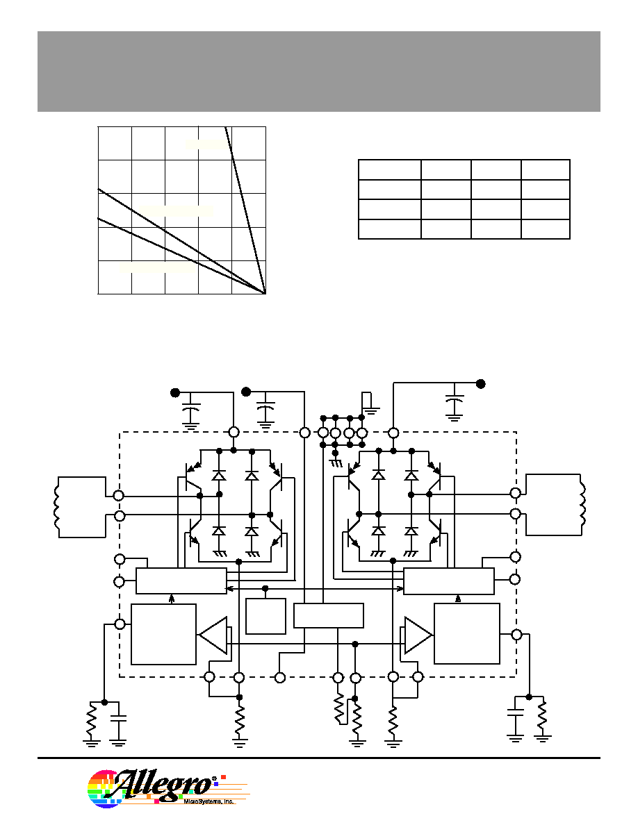
FUNCTIONAL BLOCK DIAGRAM AND TYPICAL
BIPOLAR STEPPER MOTOR APPLICATION
TRUTH TABLE
ENABLE
PHASE
OUT
A
OUT
B
H
X
Off
Off
L
H
H
L
L
L
L
H
X = Irrelevant
OUT
OUT
C
OUT
ENABLE 1
PHASE 1
CONTROL LOGIC
AND LEVEL SHIFT
OUT
1A
1B
V
BB2
BB2
C
2A
2B
S1
REF
R
R
R
R
S2
1
OUT
IN
REF
SENSE
2
2
BLANKING
TIME AND
SOURCE
DRIVER T
CONTROL
OFF
UVLO
AND
TSD
CONTROL LOGIC
AND LEVEL SHIFT
BLANKING
TIME AND
SOURCE
DRIVER T
CONTROL
OFF
VOLTAGE
REFERENCE
+
_
MOTOR SUPPLY 2
MOTOR SUPPLY 1
C
V
cc
cc
LOGIC SUPPLY
C
V
BB
BB1
GND
C
T2
R
T2
RC
2
E
2
I
FULL/PD
E
2
R
T1
T1
RC1
+
_
SENSE 1
ENABLE 2
PHASE 2
E
1
Dwg. GP-049A
50
75
100
125
150
5
1
0
ALLOWABLE PACKAGE POWER DISSIPATION IN WATTS
TEMPERATURE IN
∞
C
4
3
2
25
R = 6.0
∞
C/W
JT
SUFFIX 'B', R = 40
∞
C/W
JA
SUFFIX 'LB', R = 55
∞
C/W
JA
Copyright ©1995, 1996, Allegro MicroSystems, Inc.

3961
DUAL FULL-BRIDGE
PWM MOTOR DRIVER
Load Supply Voltage Range
V
BB
Operating, I
OUT
=
±
800 mA, L = 3 mH
5.0
--
45
V
Output Leakage Current
I
CEX
V
OUT
= V
BB
--
<1.0
50
µ
A
V
OUT
= 0 V
--
<-1.0
-50
µ
A
Output Saturation Voltage
V
CE(SAT)
Source Driver, I
OUT
= -500 mA
--
1.0
1.2
V
Source Driver, I
OUT
= -750 mA
--
1.1
1.3
V
Source Driver, I
OUT
= -800 mA
--
--
1.4
V
Sink Driver, I
OUT
= +500 mA
--
0.3
0.6
V
Sink Driver, I
OUT
= +750 mA
--
0.5
0.9
V
Sink Driver, I
OUT
= +800 mA
--
--
1.0
V
Clamp Diode Forward Voltage
V
F
I
F
= 500 mA
--
1.1
1.4
V
(Sink or Source)
I
F
= 750 mA
--
1.3
1.6
V
I
F
= 800 mA
--
--
1.7
V
Motor Supply Current
I
BB(ON)
V
ENABLE
= 0.8 V
--
5.0
7.0
mA
(No Load)
I
BB(OFF)
V
ENABLE
= 2.4 V
--
5.0
7.0
mA
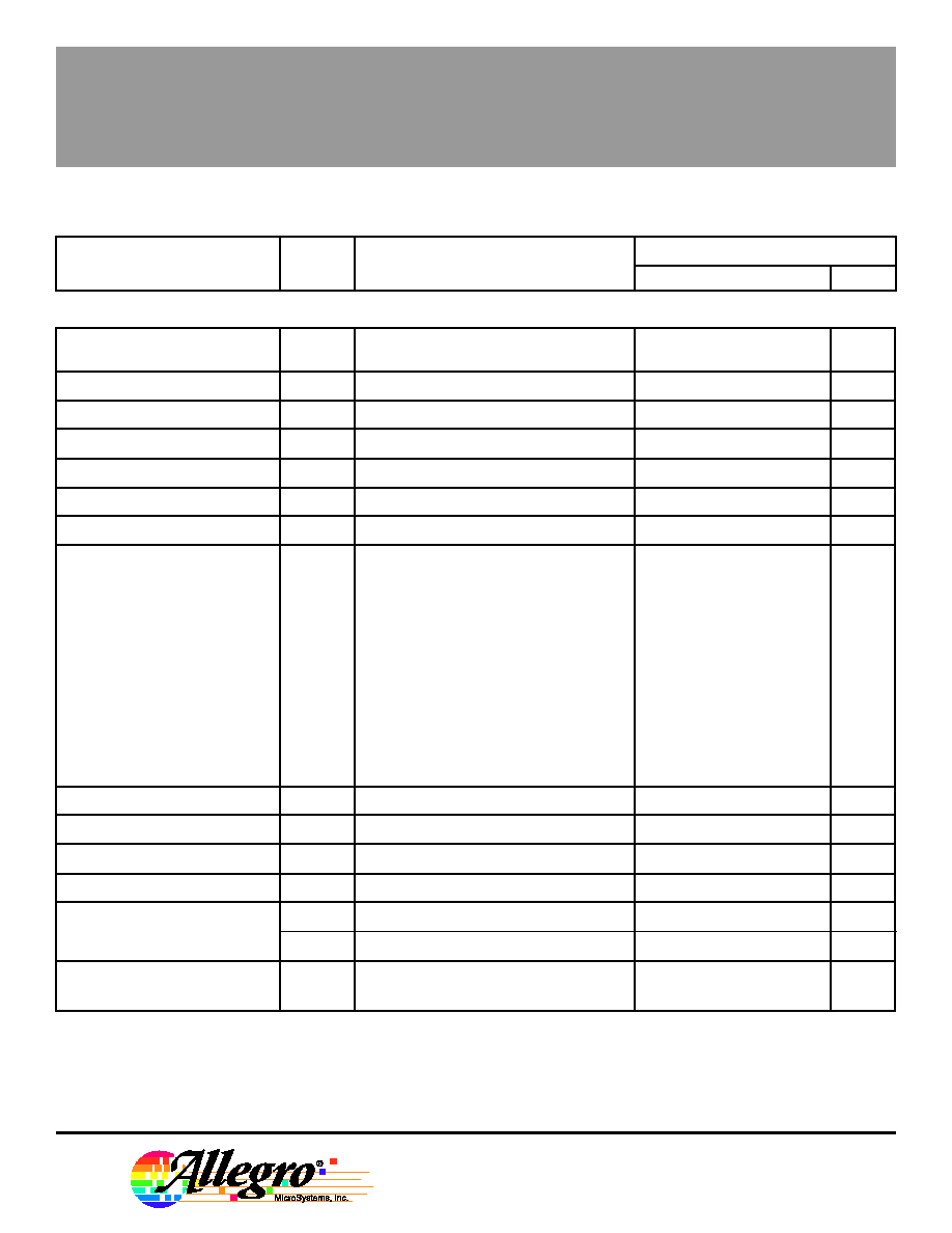
ELECTRICAL CHARACTERISTICS at T
A
= +25
∞
C, V
BB
= 45 V, V
CC
= 4.75 V to 5.25 V, V
SENSE
= 0
V, 30 k
& 1000 pF RC to Ground (unless noted otherwise)
Limits
Characteristic
Symbol
Test Conditions
Min.
Typ.
Max.
Units
Output Drivers
Continued next page...
Logic Supply Voltage Range
V
CC
Operating
4.75
--
5.25
V
Logic Input Voltage
V
IN(1)
2.4
--
--
V
V
IN(0)
--
--
0.8
V
Logic Input Current
I
IN(1)
V
IN
= 2.4 V
--
<1.0
20
µ
A
I
IN(0)
V
IN
= 0.8 V
--
<-2.0
-200
µ
A
Reference Output Voltage
V
REF OUT
V
CC
= 5.0 V, I
REF OUT
= 90 to 900
µ
A:
I
FULL/PD
= LOW
2.45
2.50
2.55
V
I
FULL/PD
= HIGH
1.49
1.67
1.84
V
Control Logic
3961
DUAL FULL-BRIDGE
PWM MOTOR DRIVER
115 Northeast Cutoff, Box 15036
Worcester, Massachusetts 01615-0036 (508) 853-5000
ELECTRICAL CHARACTERISTICS at T
A
= +25
∞
C, V
BB
= 45 V, V
CC
= 4.75 V to 5.25 V, V
SENSE
= 0
V, 30 kW & 1000 pF RC to Ground (unless noted otherwise) (cont.)
Limits
Characteristic
Symbol
Test Conditions
Min.
Typ.
Max.
Units
Reference Output Current
I
REF OUT
3 k
R
D
= R
1
+ R
2
15 k
90
--
900
µ
A
Ref. Input Offset Current
I
OS
V
REF IN
= 1 V
-2.5
0
1.0
µ
A
Comparator Input Offset Volt.
V
IO
V
REF
= 0 V
-5.0
0
5.0
mV
Comparator Input Volt. Range
V
REF
Operating
-0.3
--
1.0
V
PWM RC Fixed Off-time
t
OFF RC
C
T
= 1000 pF, R
T
= 30 k
27
30
33
µ
s
PWM Propagation Delay Time
t
PWM
Comparator Trip to Source OFF
--
1.2
2.0
µ
s
PWM Minimum On Time
t
ON(min)
C
T
= 1000 pF
±
5%, R
T
15 k
, V
CC
= 5 V
--
2.5
3.6
µ
s
Propagation Delay Times
t
pd
I
OUT
=
±
800 mA, 50% to 90%:
ENABLE ON to Source ON
--
3.2
--
µ
s
ENABLE OFF to Source OFF
--
1.2
--
µ
s
ENABLE ON to Sink ON
--
3.2
--
µ
s
ENABLE OFF to Sink OFF
--
0.7
--
µ
s
PHASE Change to Sink ON
--
3.2
--
µ
s
PHASE Change to Source ON
--
3.2
--
µ
s
PHASE Change to Sink OFF
--
0.7
--
µ
s
PHASE Change to Source OFF
--
1.2
--
µ
s
Thermal Shutdown Temp.
T
J
--
165
--
∞C
Thermal Shutdown Hysteresis
T
J
--
15
--
∞C
UVLO Disable Threshold
2.5
2.7
2.9
V
UVLO Hysterisis
0.7
0.9
1.1
V
Logic Supply Current
I
CC(ON)
V
ENABLE1
= V
ENABLE2
= 0.8 V
--
65
85
mA
I
CC(OFF)
V
ENABLE1
= V
ENABLE2
= 2.4 V
--
11
15
Logic Supply Current
I
CC(ON)
V
ENABLE1
= V
ENABLE2
= 0.8 V
--
0.18
--
mA/∞C
Temperature Coefficient
Control Logic (Continued)
NOTES: 1. Typical Data is for design information only.
2. Negative current is defined as coming out of
(sourcing) the specified device terminal.

3961
DUAL FULL-BRIDGE
PWM MOTOR DRIVER
internal current-control circuitry (or by the PHASE or
ENABLE inputs). The comparator output is blanked to
prevent false over-current detections due to reverse-
recovery currents of the clamp diodes, and/or switching
transients related to distributed capacitance in the load.
During internal PWM operation, at the end of the t
OFF
time, the comparator's output is blanked and C
T
begins to
be charged from approximately 1.1 volts by an internal
current source of approximately 1 mA. The comparator
output remains blanked until the voltage on C
T
reaches
approximately 3.0 volts.
When a transition of the PHASE input occurs, C
T
is discharged to near ground during the crossover delay
time (The crossover delay time is present to prevent
simultaneous conduction of the source and sink drivers).
After the crossover delay, C
T
is charged by an internal cur-
rent source of approximately 1 mA. The comparator out-
put remains blanked until the voltage on C
T
reaches
approximately 3.0 volts.
When the device is disabled, via the ENABLE input,
C
T
is discharged to near ground. When the device is
re-enabled, C
T
is charged by an internal current source
of approximately 1 mA. The comparator output remains
blanked until the voltage on C
T
reaches approximately
3.0 volts.
The minimum recommended value for C
T
is
1000 pF. This value ensures that the blanking time is suffi-
cient to avoid false trips of the comparator under normal
operating conditions. For optimal regulation of the load
current, the above value for C
T
is recommended and the
value of R
T
can be sized to determine t
OFF
. For more infor-
mation regarding load current regulation, see below.
Load Current Regulation. Because the device operates
in a slow decay mode (2-quadrant PWM mode), there is a
limit to the lowest level that the PWM current control cir-
cuitry can regulate load current. The limitation is due to the
minimum PWM duty cycle, which is a function of the user-
selected value of t
OFF
and the minimum on-time pulse
t
ON(min)
max that occurs each time the PWM latch is reset.
If the motor is not rotating, as in the case of a stepper mo-
tor in hold/detent mode, a brush dc motor when stalled or
at startup, the worst case value of current regulation can
be approximated by:
FUNCTIONAL DESCRIPTION
Internal PWM Current Control. The A3961S-- contains
a fixed off-time pulse-width modulated (PWM) current-
control circuit that can be used to limit the load current to
a desired value. The peak value of the current limiting
(I
TRIP
) is set by the selection of an external current-sensing
resistor (R
S
) and reference input voltage (V
REF IN
).
The internal circuitry compares the voltage across the
external sense resistor to the voltage on the reference
input terminal (V
REF IN
), resulting in a transconductance
function approximated by:
The reference input voltage is typically set with a
resistor divider from V
REF OUT
. The value of V
REF OUT
can be switched from a nominal value of 2.5 V to 1.67 V
by applying a low or high logic signal respectively to the
I
FULL/PD
terminal. To ensure proper operation of the
voltage reference, the resistor divider (R
D
= R
1
+R
2
) should
have an impedance of 3 k
to 15 k
. Within this range, a
low impedance will minimize the effect of the REF IN input
offset current.
The current-control circuitry limits the load current as
follows: when the load current reaches I
TRIP
, the compara-
tor resets a latch that turns off the selected source driver.
The load inductance causes the current to recirculate
through the sink driver and flyback diode.
For each bridge, the user selects an external resistor
(R
T
) and capacitor (C
T
) to determine the time period
(t
OFF
= R
T
C
T
) during which the source driver remains dis-
abled (see "RC Fixed Off-time" below). The range of rec-
ommended values for C
T
and R
T
are 1000 pF to
1500 pF and 15 k
to 100 k
respectively. For optimal
load current regulation, C
T
is normally set to 1000 pF (see
"Load Current Regulation" below). At the end of the RC in-
terval, the source driver is enabled allowing the load cur-
rent to increase again. The PWM cycle repeats, maintain-
ing the peak load current at the desired value.
RC BLANKING. In addition to determining the fixed off-
time of the PWM control circuit, the C
T
component sets the
comparator blanking time. This function blanks the output
of the comparator when the outputs are switched by the
I
TRIP
V
REF IN
R
S
[(V
BB
- V
SAT(SOURCE+SINK)
) t
ON(min)
max] ≠ (1.05 (V
SAT(SINK)
+ V
F
) t
OFF
)
1.05 (t
ON(min)
max + t
OFF
) R
LOAD
I
AVG