 | –≠–ª–µ–∫—Ç—Ä–æ–Ω–Ω—ã–π –∫–æ–º–ø–æ–Ω–µ–Ω—Ç: 3974 | –°–∫–∞—á–∞—Ç—å:  PDF PDF  ZIP ZIP |

Data Sheet
29319.35
3974
DMOS DUAL FULL-BRIDGE
PWM MOTOR DRIVER
Designed for pulse-width modulated (PWM) current control
of two dc motors, the A3974SED is capable of output currents to
±
1.5 A and operating voltages to 50 V. Internal fixed off-time
PWM current-control timing circuitry can be programmed via a
serial interface to operate in slow, fast, and mixed current-decay
modes.
Independant ENABLE input terminals are provided for use in
controlling the speed and torque of each dc motor with externally
applied PWM control signals.
Synchronous rectification circuitry allows the load current to
flow through the low
r
DS(on)
of the DMOS output driver during
the current decay. This feature will eliminate the need for
external clamp diodes in most applications, saving cost and
external component count, while minimizing power dissipation.
Internal circuit protection includes thermal shutdown with
hysteresis, undervoltage monitoring of V
DD
and the charge
pump, and crossover-current protection. Special power-up
sequencing is not required.
The A3974SED is supplied in a 44-lead plastic PLCC with
four copper batwing tabs for maximum heat dissipation. The
power tabs are at ground potential and need no electrical isola-
tion.
FEATURES
s
±
1.5 A, 50 V Continuous Output Rating
s Low
r
DS(on)
DMOS Output Drivers
s Programmable Slow, Fast, and Mixed Current-Decay Modes
s Serial-Interface Controls Chip Functions
s Synchronous Rectification for Low Power Dissipation
s Internal UVLO and Thermal Shutdown Circuitry
s Crossover-Current Protection
s Sleep and Idle Modes
ABSOLUTE MAXIMUM RATINGS
at T
A
= +25
∞
C
Load Supply Voltage, V
BB
............................ 50 V
Output Current, I
OUT
..................................
±
1.5 A
Logic Supply Voltage, V
DD
.......................... 7.0 V
Logic Input Voltage Range, V
IN
Continous ................... -0.3 V to V
DD
+ 0.3 V
t
W
< 30 ns ................... -1.0 V to V
DD
+ 1.0 V
Reference Voltage, V
REF
................................. 3 V
Sense Voltage (dc), V
S
Continous .............................................. 0.5 V
t
W
< 1
µ
s ................................................ 2.5 V
Package Power Dissipation, P
D
.................. 3.9 W
Operating Temperature Range,
T
A
......................................... -20
∞
C to +85
∞
C
Junction Temperature, T
J
......................... +150
∞
C
Storage Temperature Range,
T
S
....................................... -55
∞
C to +150
∞
C
Output current rating may be limited by duty cycle,
ambient temperature, and heat sinking. Under any set
of conditions, do not exceed the specified current rating
or a junction temperature of 150
∞
C.
Always order by complete part number: A3974SED .
SERIAL PORT
6
5
4
3
2
1
44
43
42
41
40
7
8
9
10
11
12
13
14
15
16
17
29
30
39
38
37
36
35
34
33
32
31
28
27
26
25
24
23
22
21
20
19
18
Dwg. PP-073
GND
GND
LOGIC
SUPPLY
GND
GND
SENSE
1
OUT
1A
NC
STROBE
CLOCK
DATA
GND
GND
REF
1
REF
2
NC
OUT
2A
NC
SENSE
2
GND
GND
GND
LOAD
SUPPLY
2
ENABLE
2
OUT
2B
NC
V
REG
SLEEP
OSC
GND
GND
CP
CP1
CP2
NC
OUT
1B
NC
ENABLE
1
LOAD
SUPPLY
1
GND
NC
NC
NC
NC
PROGRAM
PWM TIMER
CHARGE PUMP
˜
V
DD
V
BB1
V
BB2
˜
LOGIC
LOGIC
PROGRAM
PWM TIMER
3974
DMOS DUAL FULL-BRIDGE
PWM MOTOR DRIVER
115 Northeast Cutoff, Box 15036
Worcester, Massachusetts 01615-0036 (508) 853-5000
2
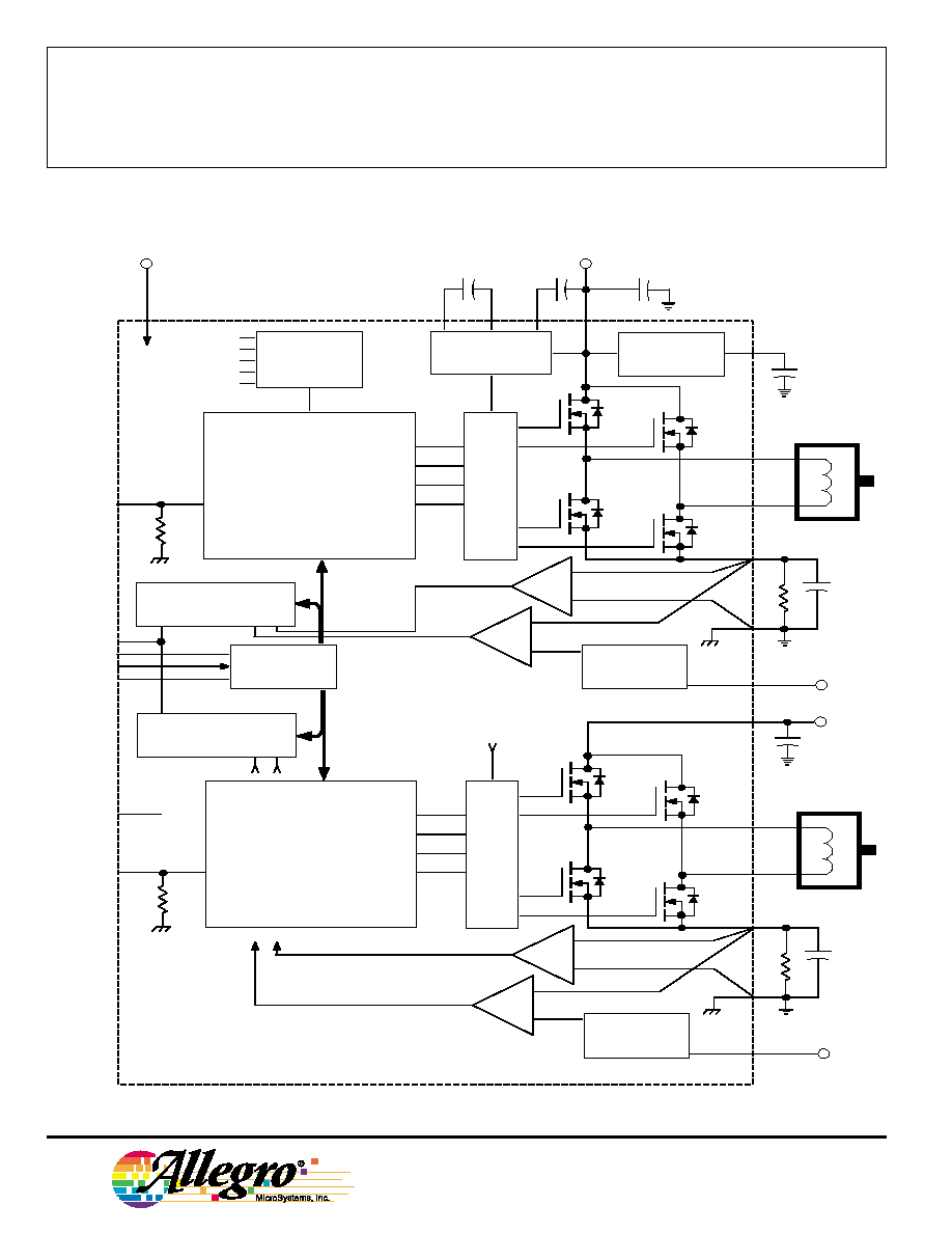
FUNCTIONAL BLOCK DIAGRAM
Copyright © 2001 Allegro MicroSystems, Inc.
CHARGE PUMP
BANDGAP
V
DD
C
REG
TSD
UNDER-
VOLTAGE &
FAULT DETECT
CHARGE
PUMP
BANDGAP
REGULATOR
V
DD
V
BB1
+
LOGIC
SUPPLY
V
REG
CP1
CP
CP2
LOAD
SUPPLY
1
GATE DRIVE
SLEEP
MODE
CONTROL LOGIC
PHASE
SYNC RECT MODE
SYNC RECT DISABLE
MODE
PROGRAMMABLE
PWM TIMER
SENSE
1
R
S1
FIXED OFF
BLANK
DECAY
ENABLE
1
OSC
CLOCK
DATA
STROBE
REFERENCE
BUFFER &
DIVIDER
OUT
1A
OUT
1B
REF
1
V
REF
C
S1
PROGRAMMABLE
PWM TIMER
FIXED OFF
BLANK
DECAY
GATE DRIVE
Dwg. FP-048-1
CONTROL LOGIC
PHASE
ENABLE
SYNC RECT MODE
SYNC RECT DISABLE
PWM MODE INT
PWM MODE EXT
SENSE
2
R
S2
ENABLE
2
REFERENCE
BUFFER &
DIVIDER
OUT
2A
OUT
2B
REF
2
V
REF2
C
S2
V
BB2
LOAD
SUPPLY
2
+
SERIAL
PORT
CHARGE
PUMP
TO PWM TIMER
ZERO CURRENT DETECT
CURRENT SENSE
ZERO CURRENT DETECT
CURRENT SENSE

3974
DMOS DUAL FULL-BRIDGE
PWM MOTOR DRIVER
3
www.allegromicro.com
ELECTRICAL CHARACTERISTICS at T
A
= +25
∞
C, V
BB
= 50 V, V
DD
= 5.0 V, f
PWM
< 50 kHz (unless
otherwise noted).
Limits
Characteristic
Symbol
Test Conditions
Min.
Typ.
Max.
Units
Output Drivers
Load Supply Voltage Range
V
BB
Operating
15
--
50
V
During sleep mode
0
--
50
V
Output Leakage Current
I
DSS
V
OUT
= V
BB
--
<1.0
20
µ
A
V
OUT
= 0 V
--
<-1.0
-20
µ
A
Output ON Resistance
r
DS(on)
Source driver, I
OUT
= -1.5 A
--
0.5
0.55
Sink driver, I
OUT
= 1.5 A
--
0.315
0.35
Body Diode Forward Voltage
V
F
Source diode, I
F
= 1.5 A
--
--
1.2
V
Sink diode, I
F
= 1.5 A
--
--
1.2
V
Load Supply Current
I
BB
f
PWM
< 50 kHz
--
4.0
7.0
mA
Charge pump on, outputs disabled
--
2.0
5.0
mA
Sleep or idle mode
--
--
20
µ
A
Control Logic
Logic Supply Voltage Range
V
DD
Operating
4.5
5.0
5.5
V
Logic Input Voltage
V
IN(1)
2.0
--
--
V
V
IN(0)
--
--
0.8
V
Logic Input Current
I
IN(1)
V
IN
= 2.0 V
--
<1.0
±
20
µ
A
(except ENABLE)
I
IN(0)
V
IN
= 0.8 V
--
<1.0
±
20
µ
A
ENABLE Input Current
I
EN(1)
V
EN
= 2.0 V
--
40
100
µ
A
I
EN(0)
V
EN
= 0.8 V
--
16
30
µ
A
OSC Input Frequency
f
OSC
2.9
--
6.1
MHz
OSC Input Duty Cycle
--
40
--
60
%
OSC Input Hysterisis
V
IN
200
--
400
mV
Reference Input Voltage Range
V
REF
Operating
0
--
2.6
V
continued next page ...

3974
DMOS DUAL FULL-BRIDGE
PWM MOTOR DRIVER
115 Northeast Cutoff, Box 15036
Worcester, Massachusetts 01615-0036 (508) 853-5000
4
Limits
Characteristic
Symbol
Test Conditions
Min.
Typ.
Max.
Units
Control Logic (continued)
Reference Input Current
I
REF
V
REF
= 2.6 V
--
--
±
1.0
µ
A
Reference Input Offset Voltage
V
IO
--
±
10
--
mV
Reference Divider Ratio
V
REF
/V
S
D16 = 1
--
10
--
--
D16 = 0
--
5.0
--
--
Gain (G
m
) Error (note 3)
E
G
V
REF
= 2.6 V, D16 = 0
--
0
±
4.0
%
V
REF
= 0.5 V, D16 = 0
--
0
±
14
%
V
REF
= 2.6 V, D16 = 1
--
0
±
4.0
%
V
REF
= 0.5 V, D16 = 1
--
0
±
10
%
Propagation Delay Time
t
pd
50% TO 90%:
PWM change to source on
600
750
1000
ns
PWM change to source off
50
150
350
ns
PWM change to sink on
600
750
1000
ns
PWM change to sink off
50
150
350
ns
Crossover Delay Time
t
COD
SR enabled
300
600
1000
ns
Thermal Shutdown Temperature
T
J
--
165
--
∞
C
Thermal Shutdown Hysteresis
T
J
--
15
--
∞
C
UVLO Enable Threshold
V
UVLO
Increasing V
DD
3.9
4.2
4.45
V
UVLO Hysteresis
V
UVLO
0.05
0.10
--
V
Logic Supply Current
I
DD
f
PWM
< 50 kHz
--
--
10
mA
Outputs off
--
--
8.0
mA
Idle mode (D18 = 1, D19 = 0)
--
--
1.5
mA
Sleep mode (inputs below 0.5 V)
--
--
100
µ
A
NOTES: 1. Typical Data is for design information only.
2. Negative current is defined as coming out of (sourcing) the specified device terminal.
3. E
G
= [(V
REF
/Range) - V
S
]/(V
REF
/Range).
ELECTRICAL CHARACTERISTICS at T
A
= +25
∞
C, V
BB
= 50 V, V
DD
= 5.0 V, f
PWM
< 50 kHz (unless
otherwise noted), continued.

3974
DMOS DUAL FULL-BRIDGE
PWM MOTOR DRIVER
5
www.allegromicro.com
Serial Interface. The A3974SED is controlled via a 3-wire
(clock, data,strobe) serial port. The programmable functions
allow maximum flexibility in configuring the PWM to the
motor drive requirements. The serial data is written as two 20-
bit words: 1 bit to select the word and 19 bits of data. The data
is clocked in starting with D19.
Word 0 Bit Assignments
Select Word 0 (D18 = 0)
Bit
Function
D0
Bridge 1 blank time LSB
D1
Bridge 1 blank time MSB
D2
Bridge 1 off-time LSB
D3
Bridge 1 off-time bit 1
D4
Bridge 1 off-time bit 2
D5
Bridge 1 off-time bit 3
D6
Bridge 1 off-time MSB
D7
Bridge 1 fast-decay time bit LSB
D8
Bridge 1 fast-decay time bit 1
D9
Bridge 1 fast-decay time bit 2
D10
Bridge 1 fast-decay time MSB
D11
Bridge 1 sync. rect. control
D12
Bridge 1 sync. rect. control
D13
Bridge 1 external PWM mode
D14
Bridge 1 enable
D15
Bridge 1 phase
D16
Bridge 1 reference range select
D17
Bridge 1 internal PWM mode
D18
Word select = 0
D19
Test mode
D0 ≠ D1 Blank Time. The current-sense comparator is
blanked when any output driver is switched on, according to the
table below. f
osc
is the oscillator input frequency.
D1
D0
Blank Time
0
0
4/f
OSC
0
1
6/f
OSC
1
0
12/f
OSC
1
1
24/f
OSC
D2 ≠ D6 Fixed Off Time. This five-bit word sets the fixed
off-time for the internal PWM control circuitry. The off-time is
defined by
t
off
=(8 [1 + N]/f
OSC
) - 1/f
OSC
where N = 0 .... 31
For example, with an oscillator frequency of 4 MHz, the
fixed off-time will be adjustable from 1.75
µ
s to 63.75
µ
s in
increments of 2
µ
s.
D7 ≠ D10 Fast Decay Time. This four-bit word sets the fast-
decay portion of the fixed off-time for the internal PWM control
circuitry. This will only have impact if mixed-decay mode is
selected (via bit D17). For t
fd
> t
off
, the device will effectively
operate in fast-decay mode. The fast-decay portion is defined
by
t
fd
= (8[1 + N]/f
OSC
] - 1/f
OSC
where N = 0 .... 15
For example, with an oscillator frequency of 4 MHz, the fast-
decay time will be adjustable from 1.75
µ
s to 31.75
µ
s in
increments of 2
µ
s.
D11 ≠ D12 Synchronous Rectification.
D12
D11
Synchronous Rectifier
0
0
Disabled
0
1
Low side only
1
0
Active
1
1
Passive
The different modes of operation are described in the synchro-
nous rectification section of the functional description.
D13 External PWM Decay Mode. This bit determines the
current-decay mode when using ENABLE chopping for
external PWM current control.
D13
Mode
0
Fast
1
Slow
FUNCTIONAL DESCRIPTION
continued next page ...