Data Sheet
26186.121
8-BIT ADDRESSABLE
DMOS POWER DRIVER
The A6A259KA and A6A259KLB combine a 3-to-8 line CMOS
decoder and accompanying data latches, control circuitry, and DMOS
outputs in a multi-functional power driver capable of storing single-line
data in the addressable latches or use as a decoder or demuliplexer.
Driver applications include relays, solenoids, and other medium-current
or high-voltage peripheral power loads.
The CMOS inputs and latches allow direct interfacing with micro-
processor-based systems. Use with TTL may require appropriate pull-
up resistors to ensure an input logic high. Four modes of operation are
selectable with the CLEAR and ENABLE inputs.
The addressed DMOS output inverts the DATA input with all
unaddressed outputs remaining in their previous states. All of the output
drivers are disabled (the DMOS sink drivers turned off) with the
CLEAR input low and the ENABLE input high. The A6A259KA/KLB
DMOS open-drain outputs are capable of sinking up to 500 mA.
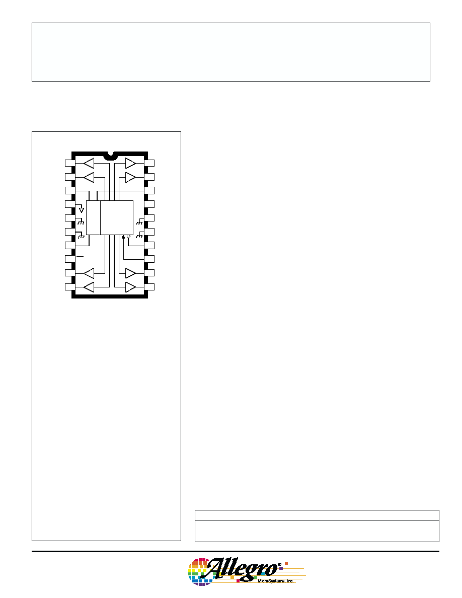
The A6A259KA is furnished in a 20-pin dual in-line plastic pack-
age. The A6A259KLB is furnished in a 24-lead wide-body, small-
outline plastic batwing package (SOIC) with gull-wing leads for surface-
mount applications. Copper lead frames, reduced supply current re-
quirements, and low on-state resistance allow both devices to sink 150
mA from all outputs continuously, to ambient temperatures over 85
�C.
FEATURES
I 50 V Minimum Output Clamp Voltage
I 350 mA Output Current (all outputs simultaneously)
I 1 Typical
r
DS(on)
I Internal Short-Circuit Protection
I Low Power Consumption
I Replacements for TPIC6A259N and TPIC6A259DW
6A259
ADVANCE INFORMATION
(Subject to change without notice)
March 22, 2000
LOGIC
GROUND
S
1
OUT
3
V
DD
POWER
GROUND
CLEAR
Dwg. PP-050-4
OUT
2
POWER
GROUND
ENABLE
EN
POWER
GROUND
S
2
(MSB)
OUT
5
OUT
4
POWER
GROUND
OUT
0
OUT
1
S
0
(LSB)
LOGIC
SUPPLY
OUT
6
OUT
7
DATA
DECODER
LATCHES
13
14
15
16
17
19
12
18
20
11
1
2
3
8
9
4
5
6
7
10
ABSOLUTE MAXIMUM RATINGS
at T
A
= 25
�
C
Output Voltage, V
O
............................ 50 V
Output Drain Current,
Continuous, I
O
...................... 350 mA*
Peak, I
OM
........................... 1100 mA*
Peak, I
OM
.................................... 2.0 A
Single-Pulse Avalanche Energy,
E
AS
............................................. 75 mJ
Logic Supply Voltage, V
DD
.............. 7.0 V
Input Voltage Range,
V
I
............................... -0.3 V to +7.0 V
Package Power Dissipation,
P
D
....................................... See Graph
Operating Temperature Range,
T
A
............................. -40
�
C to +125
�
C
Storage Temperature Range,
T
S
............................. -55
�
C to +150
�
C
*Each output, all outputs on.
Pulse duration
100 �s, duty cycle 2%.
Caution: These CMOS devices have input static
protection (Class 3) but are still susceptible to dam-
age if exposed to extremely high static electrical
charges.
Always order by complete part number:
Part Number
Package
R
JA
R
JC
R
JT
A6A259KA
20-pin DIP55
�C/W
25
�C/W
--
A6A259KLB
24-lead SOIC
55
�C/W
--
6
�C/W
A6A259KA (DIP)
6A259
8-BIT ADDRESSABLE
DMOS POWER DRIVER
115 Northeast Cutoff, Box 15036
Worcester, Massachusetts 01615-0036 (508) 853-5000
Copyright � 2000, Allegro MicroSystems, Inc.
FUNCTION TABLE
Inputs
Addressed
Other
CLEAR ENABLE DATA
OUTPUT
OUTPUTs
Function
H
L
H
L
R
Addressable
H
L
L
H
R
Latch
H
H
X
R
R
Memory
L
L
H
L
H
8-Line
L
L
L
H
H
Demultiplexer
L
H
X
H
H
Clear
L = Low Logic Level H = High Logic Level X = Irrelevant R = Previous State
LATCH SELECTION TABLE
Select Inputs
Addressed
S
2
(
MSB
) S
1
S
0
(
LSB
)
OUTPUT
L
L
L
0
L
L
H
1
L
H
L
2
L
H
H
3
H
L
L
4
H
L
H
5
H
H
L
6
H
H
H
7
DMOS POWER DRIVER OUTPUT
LOGIC INPUTS
Dwg. EP-063-5
OUT
IN
Dwg. EP-010-15
V
DD
A6A259KLB (SOIC)
POWER
GROUND
CLEAR
POWER
GROUND
ENABLE
EN
POWER
GROUND
S
2
(MSB)
OUT
5
OUT
4
POWER
GROUND
OUT
6
OUT
7
DATA
LOGIC
GROUND
S
1
OUT
3
V
DD
POWER
GROUND
OUT
2
POWER
GROUND
POWER
GROUND
POWER
GROUND
OUT
0
OUT
1
S
0
(LSB)
LOGIC
SUPPLY
DECODER
LATCHES
Dwg. PP-050-3A
1
2
3
8
17
18
19
20
21
23
4
5
6
7
22
24
12
9
10
11
13
14
15
16
50
75
100
125
150
5
1
0
ALLOWABLE PACKAGE POWER DISSIPATION IN WATTS
TEMPERATURE IN
�C
4
3
2
25
Dwg. GP-049-5
SUFFIX 'LB', R = 6.0
�C/W
JT
R = 55
�C/W
JA
SUFFIX 'A', R = 25
�C/W
JC
6A259
8-BIT ADDRESSABLE
DMOS POWER DRIVER
www.allegromicro.com
Power grounds must be connected externally to a single point.
V
DD
LOGIC
SUPPLY
DATA
CLEAR
(ACTIVE LOW)
ENABLE
(ACTIVE LOW)
2
S
(MSB)
1
S
0
S
(LSB)
LOGIC
GROUND
POWER
GROUND
Dwg. FP-047-2
OUT
0
D
C1
CLR
OUT
1
D
C1
CLR
OUT
2
D
C1
CLR
OUT
3
D
C1
CLR
OUT
4
D
C1
CLR
OUT
5
D
C1
CLR
OUT
6
D
C1
CLR
OUT
7
D
C1
CLR
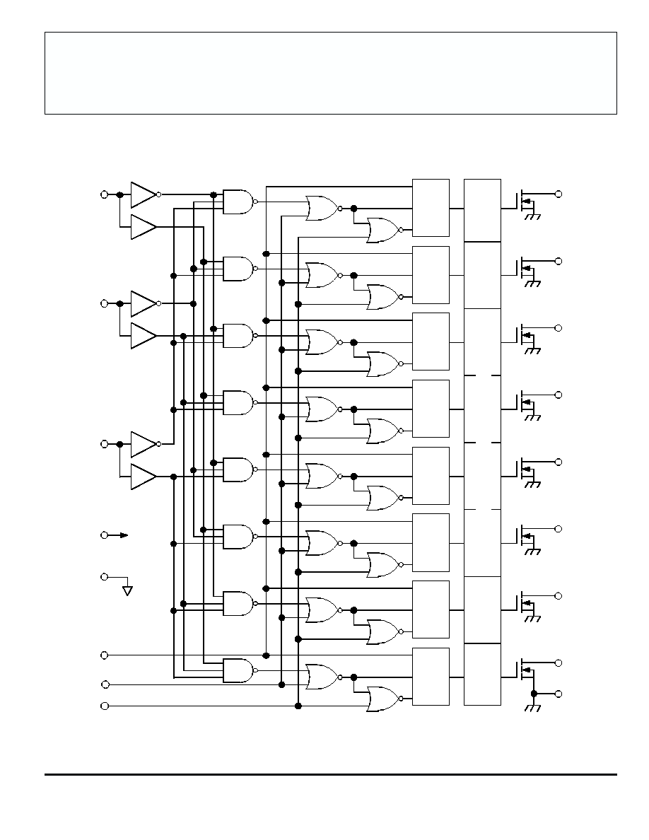
CURRENT LIMIT AND CHARGE PUMP
FUNCTIONAL BLOCK DIAGRAM
6A259
8-BIT ADDRESSABLE
DMOS POWER DRIVER
115 Northeast Cutoff, Box 15036
Worcester, Massachusetts 01615-0036 (508) 853-5000
Limits
Characteristic
Symbol
Test Conditions
Min.
Typ.
Max.
Units
Logic Supply Voltage
V
DD
Operating
4.5
5.0
5.5
V
Output Breakdown
V
(BR)DSX
I
O
= 1 mA
50
--
--
V
Voltage
Off-State Output
I
DSX
V
O
= 40 V
--
0.1
1.0
�A
Current
V
O
= 40 V, T
A
= 125
�C
--
0.2
5.0
�A
Static Drain-Source
r
DS(on)
I
O
= 350 mA
--
1.0
1.5
On-State Resistance
I
O
= 350 mA, T
A
= 125
�C
--
1.7
2.5
Source-to-Drain
V
SD
I
F
= 350 mA
--
1.0
--
V
Diode Voltage
Nominal Output
I
O(nom)
V
DS(on)
= 0.5 V, T
A
= 85
�C
--
350
--
mA
Current
Output Current
I
O(chop)
I
O
at which chopping starts, T
C
= 25
�C
0.6
0.8
1.1
A
Logic Input Current
I
IH
V
I
= V
DD
= 5.5 V
--
--
1.0
�A
I
IL
V
I
= 0, V
DD
= 5.5 V
--
--
-1.0
�A
Prop. Delay Time
t
PLH
I
O
= 350 mA, C
L
= 30 pF
--
100
--
ns
t
PHL
I
O
= 350 mA, C
L
= 30 pF
--
60
--
ns
Output Rise Time
t
r
I
O
= 350 mA, C
L
= 30 pF
--
55
--
ns
Output Fall Time
t
f
I
O
= 350 mA, C
L
= 30 pF
--
40
--
ns
Supply Current
I
DD(off)
V
DD
= 5.5 V, Outputs OFF
--
15
100
�A
I
DD(on)
V
DD
= 5.5 V, Outputs ON
--
150
300
�A
Typical Data is at V
DD
= 5 V and is for design information only.
NOTE -- Pulse test, duration
100 �s, duty cycle 2%.
ELECTRICAL CHARACTERISTICS at T
A
= +25
�
C, V
DD
= 5 V, t
ir
= t
if
10 ns (unless otherwise
specified).
RECOMMENDED OPERATING CONDITIONS
over operating temperature range
Logic Supply Voltage Range, V
DD
............... 4.5 V to 5.5 V
High-Level Input Voltage, V
IH
............................
0.85V
DD
Low-level input voltage, V
IL
.................................
0.15V
DD
6A259
8-BIT ADDRESSABLE
DMOS POWER DRIVER
www.allegromicro.com
FUNCTIONAL DESCRIPTION and INPUT REQUIREMENTS
Four modes of operation are selectable by controlling the
CLEAR and ENABLE inputs as shown above.
In the addressable-latch mode, data at the DATA input is
written into the addressed transparent latch. The addressed
output inverts the data input with all other outputs remaining
in their previous states.
In the memory mode, all outputs remain in their previous
states and are unaffected by the DATA or address (S
n
) inputs.
To prevent entering erroneus data in the latches, ENABLE
should be held HIGH while the address lines are changing.
In the demultiplexing/decoding mode, the addressed
output inverts the data input and all other outputs are OFF.
In the clear mode, all outputs are OFF and are unaffected
by the DATA or address (S
N
) inputs.
Given the appropriate inputs, when DATA is LOW for a
given address, the output is OFF; when DATA is HIGH, the
output is ON and can sink current.
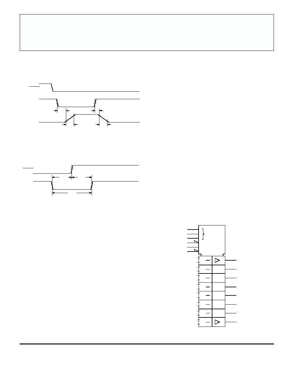
DATA INPUT REQUIREMENTS
Data Active Time Before Enable
(Data Set-Up Time), t
su(D)
.............................................. 20 ns
Data Active Time After Enable
(Data Hold Time), t
h(D)
................................................... 20 ns
Data Pulse Width, t
w(D)
....................................................... 40 ns
Input Logic High, V
IH
................................................
0.85V
DD
Input Logic Low, V
IL
.................................................
0.15V
DD
50%
Dwg. WP-037
ENABLE
DATA
50%
w(D)
t
su(D)
t
h(D)
t
PHL
t
PLH
t
50%
ADDRESSED
OUTPUT
Dwg. WP-036
10%
90%
f
t
r
t
ENABLE
DATA
OUTPUT SWITCHING TIME
LOGIC SYMBOL
G8
Z9
9,0D
10,0R
OUT
0
OUT
1
OUT
2
OUT
3
OUT
4
OUT
5
OUT
6
OUT
7
S
1
S
2
DATA
ENABLE
Dwg. FP-046-2
0
2
S
0
CLEAR
Z10
8M 0/7
9,1D
10,1R
9,2D
10,2R
9,3D
10,3R
9,4D
10,4R
9,5D
10,5R
9,6D
10,6R
9,7D
10,7R