 | –≠–ª–µ–∫—Ç—Ä–æ–Ω–Ω—ã–π –∫–æ–º–ø–æ–Ω–µ–Ω—Ç: 6A595 | –°–∫–∞—á–∞—Ç—å:  PDF PDF  ZIP ZIP |

Data Sheet
26185.121
8-BIT SERIAL-INPUT,
DMOS POWER DRIVER
The A6A595KA and A6A595KLB combine an 8-bit CMOS shift
register and accompanying data latches, control circuitry, and DMOS
power driver outputs. Power driver applications include relays, sole-
noids, and other medium-current or high-voltage peripheral power
loads.
The serial-data input, CMOS shift register and latches allow direct
interfacing with microprocessor-based systems. Serial-data input rates
are over 5 MHz. Use with TTL may require appropriate pull-up
resistors to ensure an input logic high.
A CMOS serial-data output enables cascade connections in appli-
cations requiring additional drive lines.
The A6A595 DMOS open-drain outputs are capable of sinking up
to 500 mA. All of the output drivers are disabled (the DMOS sink
drivers turned off) by the OUTPUT ENABLE input high.
The A6A595KA is furnished in a 20-pin dual in-line plastic
package. The A6A595KLB is furnished in a 24-lead wide-body, small-
outline plastic batwing package (SOIC) with gull-wing leads. Copper
lead frames, reduced supply current requirements, and low on-state
resistance allow both devices to sink 150 mA from all outputs continu-
ously, to ambient temperatures over 85
∞C.
FEATURES
I 50 V Minimum Output Clamp Voltage
I 350 mA Output Current (all outputs simultaneously)
I 1 Typical
r
DS(on)
I Internal Short-Circuit Protection
I Low Power Consumption
I Replacements for TPIC6A595N and TPIC6A595DW
6A595
ADVANCE INFORMATION
(Subject to change without notice)
March 22, 2000
Always order by complete part number:
Part Number
Package
R
JA
R
JC
R
JT
A6A595KA
20-pin DIP55
∞C/W
25
∞C/W
--
A6A595KLB
24-lead SOIC
55
∞C/W
--
6
∞C/W
ABSOLUTE MAXIMUM RATINGS
at T
A
= 25
∞
C
Output Voltage, V
O
............................... 50 V
Output Drain Current,
Continuous, I
O
.......................... 350 mA*
Peak, I
OM
................................. 1100 mA
Single-Pulse Avalanche Energy,
E
AS
................................................. 75 mJ
Logic Supply Voltage, V
DD
.................. 7.0 V
Input Voltage Range,
V
I
................................... -0.3 V to +7.0 V
Package Power Dissipation,
P
D
........................................... See Graph
Operating Temperature Range,
T
A
................................. -40
∞
C to +125
∞
C
Storage Temperature Range,
T
S
................................. -55
∞
C to +150
∞
C
* Each output, all outputs on.
Pulse duration
100 µs, duty cycle 2%.
Caution: These CMOS devices have input static
protection (Class 3) but are still susceptible to
damage if exposed to extremely high static
electrical charges.
LATCHES
REGISTER
SERIAL
DATA IN
REGISTER
CLEAR
OUT
3
V
DD
STROBE
CLOCK
CLK
ST
Dwg. PP-029-15
OUT
2
OUTPUT
ENABLE
OE
LOGIC
GROUND
CLR
13
14
15
16
17
19
12
18
20
11
1
2
3
8
9
4
5
6
7
10
POWER
GROUND
POWER
GROUND
POWER
GROUND
POWER
GROUND
OUT
5
OUT
4
OUT
6
OUT
7
OUT
1
OUT
0
SERIAL
DATA OUT
LOGIC
SUPPLY
REGISTER
LATCHES
A6A595KA (DIP)
6A595
8-BIT SERIAL-INPUT,
DMOS POWER DRIVER
115 Northeast Cutoff, Box 15036
Worcester, Massachusetts 01615-0036 (508) 853-5000
Copyright © 2000, Allegro MicroSystems, Inc.
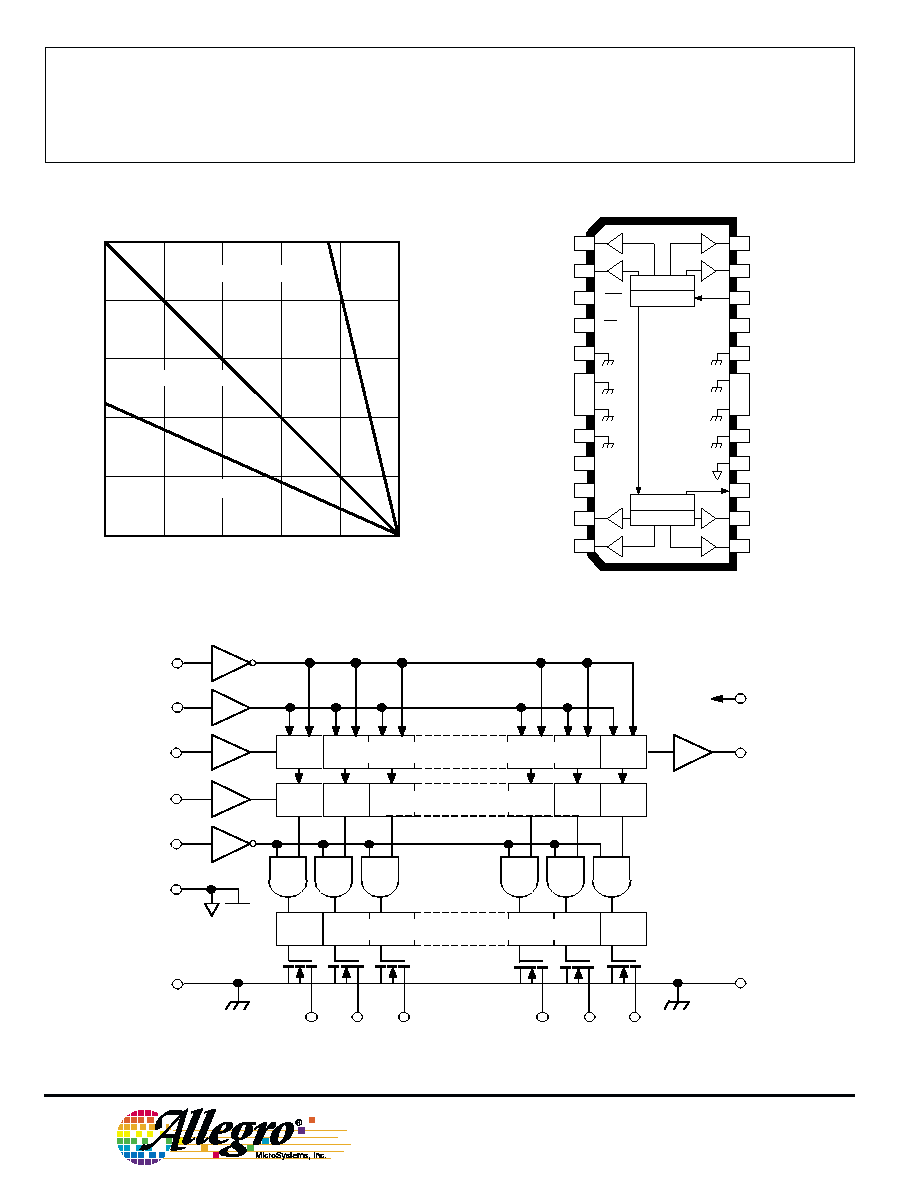
FUNCTIONAL BLOCK DIAGRAM
POWER
GROUND
Dwg. FP-013-6
OUT
0
OUT
N
POWER
GROUND
CLOCK
SERIAL
DATA IN
STROBE
OUTPUT
ENABLE
(ACTIVE LOW)
SERIAL
DATA OUT
SERIAL-PARALLEL SHIFT REGISTER
D-TYPE LATCHES
V
DD
LOGIC
SUPPLY
REGISTER
CLEAR
(ACTIVE LOW)
LOGIC
GROUND
CURRENT LIMIT AND CHARGE PUMP
SUB
Power grounds must be connected together externally.
POWER
GROUND
POWER
GROUND
POWER
GROUND
POWER
GROUND
POWER
GROUND
POWER
GROUND
POWER
GROUND
POWER
GROUND
LATCHES
REGISTER
SERIAL
DATA IN
REGISTER
CLEAR
OUT
3
V
DD
STROBE
CLOCK
CLK
ST
Dwg. PP-029-16A
OUT
2
OUTPUT
ENABLE
OE
LOGIC
GROUND
CLR
OUT
5
OUT
4
OUT
6
OUT
7
OUT
1
OUT
0
SERIAL
DATA OUT
LOGIC
SUPPLY
REGISTER
LATCHES
1
2
3
8
17
18
19
20
21
23
4
5
6
7
22
24
12
9
10
11
13
14
15
16
A6A595KLB (SOIC)
50
75
100
125
150
5
1
0
ALLOWABLE PACKAGE POWER DISSIPATION IN WATTS
TEMPERATURE IN
∞C
4
3
2
25
Dwg. GP-049-5
SUFFIX 'LB', R = 6.0
∞C/W
JT
R = 55
∞C/W
JA
SUFFIX 'A', R = 25
∞C/W
JC

6A595
8-BIT SERIAL-INPUT,
DMOS POWER DRIVER
www.allegromicro.com
TRUTH TABLE
Shift Register Contents
Serial
Latch Contents
Output Contents
Data
Clock
Data
Output
Input
Input
I
0
I
1
I
2
...
I
6
I
7
Output Strobe
I
0
I
1
I
2
...
I
6
I
7
Enable
I
0
I
1
I
2
...
I
6
I
7
H
H
R
0
R
1
...
R
5
R
6
R
6
L
L
R
0
R
1
...
R
5
R
6
R
6
X
R
0
R
1
R
2
...
R
6
R
7
R
7
X
X
X
...
X
X
X
--
R
0
R
1
R
2
...
R
6
R
7
P
0
P
1
P
2
...
P
6
P
7
P
7
P
0
P
1
P
2
...
P
6
P
7
L
P
0
P
1
P
2
...
P
6
P
7
X
X
X
...
X
X
H
H
H
H
...
H
H
L = Low Logic Level H = High Logic Level X = Irrelevant P = Present State R = Previous State
SERIAL DATA OUT
LOGIC INPUTS
Dwg. EP-063-4
OUT
V
DD
DMOS POWER DRIVER OUTPUT
Dwg. EP-010-10
IN
V
DD
Dwg. EP-063-5
OUT
RECOMMENDED OPERATING CONDITIONS
over operating temperature range
Logic Supply Voltage Range, V
DD
............... 4.5 V to 5.5 V
High-Level Input Voltage, V
IH
............................
0.85V
DD
Low-level input voltage, V
IL
.................................
0.15V
DD

6A595
8-BIT SERIAL-INPUT,
DMOS POWER DRIVER
115 Northeast Cutoff, Box 15036
Worcester, Massachusetts 01615-0036 (508) 853-5000
Limits
Characteristic
Symbol
Test Conditions
Min.
Typ.
Max.
Units
Output Breakdown
V
(BR)DSX
I
O
= 1 mA
50
--
--
V
Voltage
Off-State Output
I
DSX
V
O
= 40 V
--
0.1
1.0
µA
Current
V
O
= 40 V, T
A
= 125
∞C
--
0.2
5.0
µA
Static Drain-Source
r
DS(on)
I
O
= 350 mA
--
1.0
1.5
On-State Resistance
I
O
= 350 mA, T
A
= 125
∞C
--
1.7
2.5
Source-to-Drain
V
SD
I
F
= 350 mA
--
1.0
--
V
Diode Voltage
Nominal Output
I
O(nom)
V
DS(on)
= 0.5 V, T
A
= 85
∞C
--
350
--
mA
Current
Output Current
I
O(chop)
I
O
at which chopping starts, T
C
= 25
∞C
0.6
0.8
1.1
A
Logic Input Current
I
IH
V
I
= V
DD
--
--
1.0
µA
I
IL
V
I
= 0
--
--
-1.0
µA
SERIAL-DATA
V
OH
I
OH
= -20
µA
4.9
4.99
--
V
Output Voltage
I
OH
= -4 mA
4.5
4.7
--
V
V
OL
I
OL
= 20
µA
--
0
0.1
V
I
OL
= 4 mA
--
0.3
0.5
V
Prop. Delay Time
t
PLH
I
O
= 350 mA, C
L
= 30 pF
--
100
--
ns
t
PHL
I
O
= 350 mA, C
L
= 30 pF
--
60
--
ns
Output Rise Time
t
r
I
O
= 350 mA, C
L
= 30 pF
--
55
--
ns
Output Fall Time
t
f
I
O
= 350 mA, C
L
= 30 pF
--
40
--
ns
Supply Current
I
DD(off)
Outputs OFF
--
0.5
5.0
mA
I
DD(fclk)
f
clk
= 5 MHz, C
L
= 30 pF, Outputs OFF
--
--
1.3
mA
Typical Data is at V
DD
= 5 V and is for design information only.
NOTE -- Pulse test, duration
100 µs, duty cycle 2%.
ELECTRICAL CHARACTERISTICS at T
A
= +25
∞
C, V
DD
= 5 V, t
ir
= t
if
10 ns (unless otherwise
specified).

6A595
8-BIT SERIAL-INPUT,
DMOS POWER DRIVER
www.allegromicro.com
TIMING REQUIREMENTS and SPECIFICATIONS
(Logic Levels are V
DD
and Ground)
CLOCK
SERIAL
DATA IN
STROBE
OUTPUT
ENABLE
OUT
N
Dwg. WP-029-2
50%
SERIAL
DATA OUT
DATA
DATA
50%
50%
50%
C
A
B
D
E
LOW = ALL OUTPUTS ENABLED
p
t
DATA
50%
p
t
LOW = OUTPUT ON
HIGH = OUTPUT OFF
OUTPUT
ENABLE
OUT
N
Dwg. WP-030-2
DATA
10%
50%
PHL
t
PLH
t
HIGH = ALL OUTPUTS DISABLED
90%
f
t
r
t
A. Data Active Time Before Clock Pulse
(Data Set-Up Time), t
su(D)
.......................................... 20 ns
B. Data Active Time After Clock Pulse
(Data Hold Time), t
h(D)
.............................................. 20 ns
C. Clock Pulse Width, t
w(CLK)
............................................. 40 ns
D. Time Between Clock Activation
and Strobe, t
su(ST)
....................................................... 50 ns
E. Strobe Pulse Width, t
w(ST)
.............................................. 50 ns
F. Output Enable Pulse Width, t
w(OE)
................................ 4.5
µ
s
NOTE ≠ Timing is representative of a 12.5 MHz clock.
Higher speeds are attainable.
Serial data present at the input is transferred to the shift
register on the rising edge of the CLOCK input pulse. On
succeeding CLOCK pulses, the registers shift data information
towards the SERIAL DATA OUTPUT.
Information present at any register is transferred to the
respective latch on the rising edge of the STROBE input pulse
(serial-to-parallel conversion).
When the OUTPUT ENABLE input is high, the output
source drivers are disabled (OFF). The information stored in the
latches is not affected by the OUTPUT ENABLE input. With
the OUTPUT ENABLE input low, the outputs are controlled by
the state of their respective latches.
LOGIC SYMBOL
2
G3
C2
SRG8
C1
R
1D
2
OUT
0
OUT
1
OUT
2
OUT
3
OUT
4
OUT
5
OUT
6
OUT
7
SERIAL
DATA OUT
OUTPUT
ENABLE
STROBE
REGISTER
CLEAR
SERIAL
DATA IN
CLOCK
Dwg. FP-043-2